Article

Patterned Graphene-Based Metamaterials for Terahertz Wave Absorption

1
Key Laboratory of National Defense Science and Technology on Electronic Measurement, School of Instrument and Electronics, North University of China, Taiyuan 030051, China
2
School of Mechanical Engineering, North University of China, Taiyuan 030051, China
3
Sichuan Jiuzhou Electric Group Co., Ltd., Mianyang 621000, China
*
Authors to whom correspondence should be addressed.
Coatings 2023, 13(1), 59; https://doi.org/10.3390/coatings13010059
Submission received: 2 December 2022 / Revised: 22 December 2022 / Accepted: 23 December 2022 / Published: 29 December 2022
(This article belongs to the Special Issue Micro-Nano Optics and Its Applications)

Abstract

:
Graphene-based metamaterials have been widely applied in optoelectronic devices, optical modulators, and chemical sensors due to the outstanding tunability and optical response in the terahertz (THz) region. Here, tunable THz metamaterial absorbers based on patterned graphene are designed, fabricated, and modulated. The proposed metamaterial absorbers are constructed by the top layer of patterned graphene arrays and the aluminum (Al) film separated by polyimide (PI). The different THz absorption spectra can be acquired by changing the patterns of graphene. In order to verify the simulation results, a series of tests were conducted by THz time-domain spectrometer (THz-TDS) systems. The proposed absorbers are able to be insensitive to the angle of the incident wave. Besides, chemical doping is applied to turn the Fermi level of graphene and the absorption performance is promoted with the increase of the Fermi level. The experimental results have been demonstrated to have associated resonant peaks with the simulation results. The aim of this paper is to exhibit a systematic study on graphene-based THz metamaterial absorbers, including the simulation and experiments. By comparing the simulation and experimental results, it is useful to clarify the relevant theories and manufacturing processes. The work will provide a further step in the development of high-performance terahertz devices, including tunable absorbers, sensors, and electro-optic switches.

1. Introduction

The rapid development of communication technology has been witnessed in recent years. The terahertz (THz) wave ranging from 0.1 to 10 THz has been endowed with a remarkable information-carrying capability [1]. Especially, the THz quantum cascade lasers contribute much to the developing of an electrically-pumped, semiconductor-based, high-power, compact, and easy-to-use THz source [2]. Therefore, THz technology has attracted a great deal of attention to developing novel communication [3,4,5] and radar detection technologies [6,7,8]. However, it also brings an ever-increasing electromagnetic pollution threat to human beings’ health and device reliability [9]. As a result, a large amount of research has been conducted to explore effective THz absorbers. Metamaterials, artificial subwavelength micro-units, show unprecedented electromagnetic properties in the manipulation of electromagnetic waves [10,11]. Therefore, various THz metamaterials have been proposed to realize THz wave absorption in recent years [12,13,14].
Landy et al. first proposed perfect metamaterial absorbers, which can selectively respond to THz waves with the changes of geometries of electric and magnetic resonators [15]. Planar THz metamaterial with multi-resonant frequencies was designed to achieve three distinct absorption frequencies around 0.29, 0.46, and 0.92 THz by Chen et al. [16]. Cui and his co-workers presented an ultra-broadband polarization-independent wide-angle THz semiconductor metamaterial absorber [17]. The designed absorber exhibited an outstanding THz wave absorption capability with high efficiency (>90%), reaching the ultra-broadband width from 1.6 to 5 THz. Though most proposed metamaterial absorbers realized perfect THz absorption due to the strong electromagnetic resonance, the function was restricted with the pre-designed frequency.
Therefore, many efforts have been devoted to tunable metamaterial absorbers. For example, Rafał Kowerdziej et al. tuned the intensity (up to 26.3%) and spectrum (up to 8 THz) of the metamaterial absorber of the near-infrared wave by changing the liquid crystal alignment, which can be attributed to the birefringence of the nematic liquid crystal contained in the metamaterial cavity [18]. Fathi Bendelala et al. proposed a VO2-based absorber structure in the infrared region. The designed absorber characteristics can be effectively controlled via the VO2 transition from semiconductor to metallic states. [19]
Graphene has been demonstrated to have superior mechanical properties [20,21], electronic effects [22], and optical properties [23,24] since it was discovered by Andre Geim and Konstantin Novoselov in 2004 [25]. Besides, graphene was found to support surface plasmons (SPs) in the THz region as well as the infrared region [26,27,28,29]. What’s more, the Fermi level of graphene can be tuned by chemical doping [30] or electrical gating [31,32]. Therefore, graphene has been widely adopted to prepare tunable THz metamaterial absorbers [33,34,35,36].
Wang et al. proposed a dynamically tunable dual-band own THz metamaterial based on graphene, which realized perfect absorption at the frequency of 7.1 and 10.4 THz [37]. Specifically, the designed THz metamaterial, consisting of a periodic array of two sizes of graphene disks on a lossless dielectric thin layer with a metal film at the bottom, showed independence to the angle of the incident wave. Xiao designed tunable THz absorbers benefitting from the graphene’s surface plasmon resonances [38]. Moreover, the effect of the geometrical parameters and Fermi level of surface graphene were investigated to realize the broadband THz absorber. Sun and his team reported the broadband and tunable THz wave absorber consisting of a graphene metasurface and a metallic mirror separated by a thin SiO2 spacer [39]. The designed THz wave absorber successfully achieved a larger working bandwidth and insensitivity to both the incident angle and polarization of the THz wave. However, most of the above research is limited in its simulation without carrying out experiments.
Compared to previous works that were limited in their design and simulation, we went further by fabricating THz metamaterial absorbers composed of a periodic array of various graphene patterns and a metal film separated by a thin PI spacer. The designed absorbers achieve dual-band effective absorption and tunability owing to the changes of patterns and the Fermi level. Besides, the absorption performance of the fabricated metamaterial absorbers with multiple graphene patterns is measured via the THz-TDS system. The experimental results exhibit a relevant trend between the simulation and experimental absorption curves, which verifies the accuracy of the fabricated device to some extent. Furthermore, the absorption mechanism is explored by analyzing the relative impedance and electric field distribution which is generated by the simulation. More importantly, the absorption peaks can be conveniently modulated in a particular manner by applying chemical doping on the graphene patch.

2. Structure Design and Fabrication

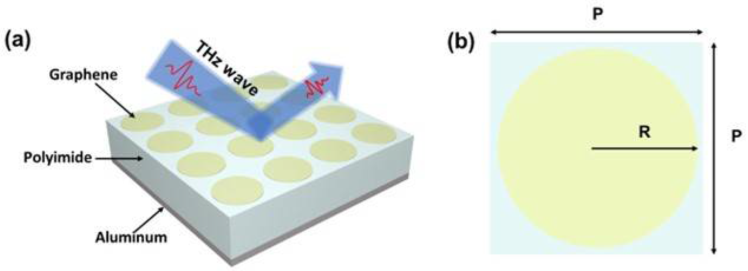
2.1. Geometry and Principle of the Proposed Graphene Absorbers

As shown in Figure 1a, the proposed graphene-based metamaterial absorber is constructed using a single layer of patterned graphene and a 200 nm thick Al film separated by a PI spacer with a thickness of 25 μm. It is depicted in Figure 1b that the top graphene layer consists of a disk-patterned array with a radius R of 35 μm. The periodic unit of the designed metamaterial is set as P = 100 μm. The refractive index of the PI layer is 2.2 and the conductivity of the Al ground plate is 3.5 × 10⁷ S/m, which achieves perfect reflection in the THz frequency region.
According to the well-known Kubo formula, the surface conductivity of graphene ( σ gra ), including intraband conductivity ( σ intra ) and interband conductivity ( σ inter ), is given as follows [40,41]:
σ gra = σ intra + σ inter = 2 e 2 k B T π ħ 2 i ω + i / τ ln [ 2 cos   h ( E f 2 k B T ) ] + e 2 4 ħ 2 [ 1 2 + 1 π arctan ( ħ ω 2 E f 2 k B T ) i 2 π ln ( ħ ω + 2 E f ) 2 ( ħ ω 2 E f ) 2 + 4 ( k B T ) 2 ]
where ω is the frequency, τ stands for the relaxation time, E f is the Fermi level, T is the absolute temperature of the environment, k B represents the Boltzmann constant, and e and ħ stand for electron charge and reduced Plank constant ( ħ = h / 2 π ), respectively. The corresponding detailed parameters are shown in Table 1. According to the Pauli exclusion principle, the interband transition is small enough to be negligible in the THz frequency region. As a result, the Kubo formula can be simplified to the Drude model to calculate the surface conductivity of graphene with the following equation:
σ g r a = e 2 E f π ħ 2 i ( ω + i / τ )
In this study, commercial software COMSOL Multiphysics is adopted to illustrate the absorption performance of the proposed metamaterial absorbers. In the numerical simulations, the electric field of the incident THz wave is polarized along the x direction and the unit cell is set as the periodic boundary condition. In order to improve the efficiency and accuracy of simulations, the graphene layer is regarded as a transition boundary condition due to the ultra-thin thickness of graphene. By using the frequency domain solver to calculate the S parameter, the absorptivity A can be expressed by [42]:
A = 1 R T = 1 |   S 11   | 2 |   S 21   | 2
where R and T represent reflectivity and transmissivity, respectively. Since the thickness of the Al film exceeds the skinning depth, the transmittance can be ignored. Hence, the absorptivity can be simplified to the following equation [43]:
A = 1 R = 1 |   S 11   | 2  

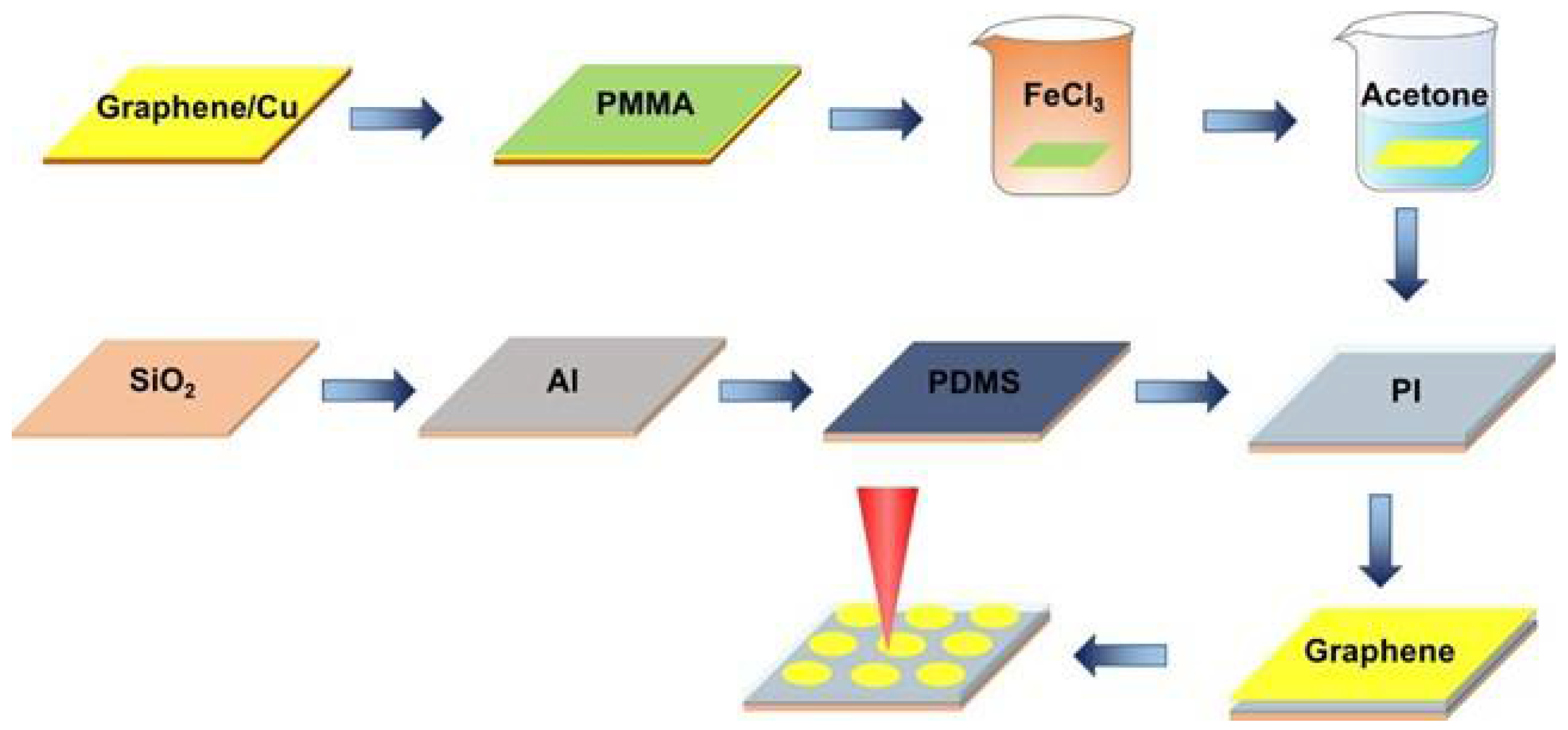
2.2. Device Fabrication and Test
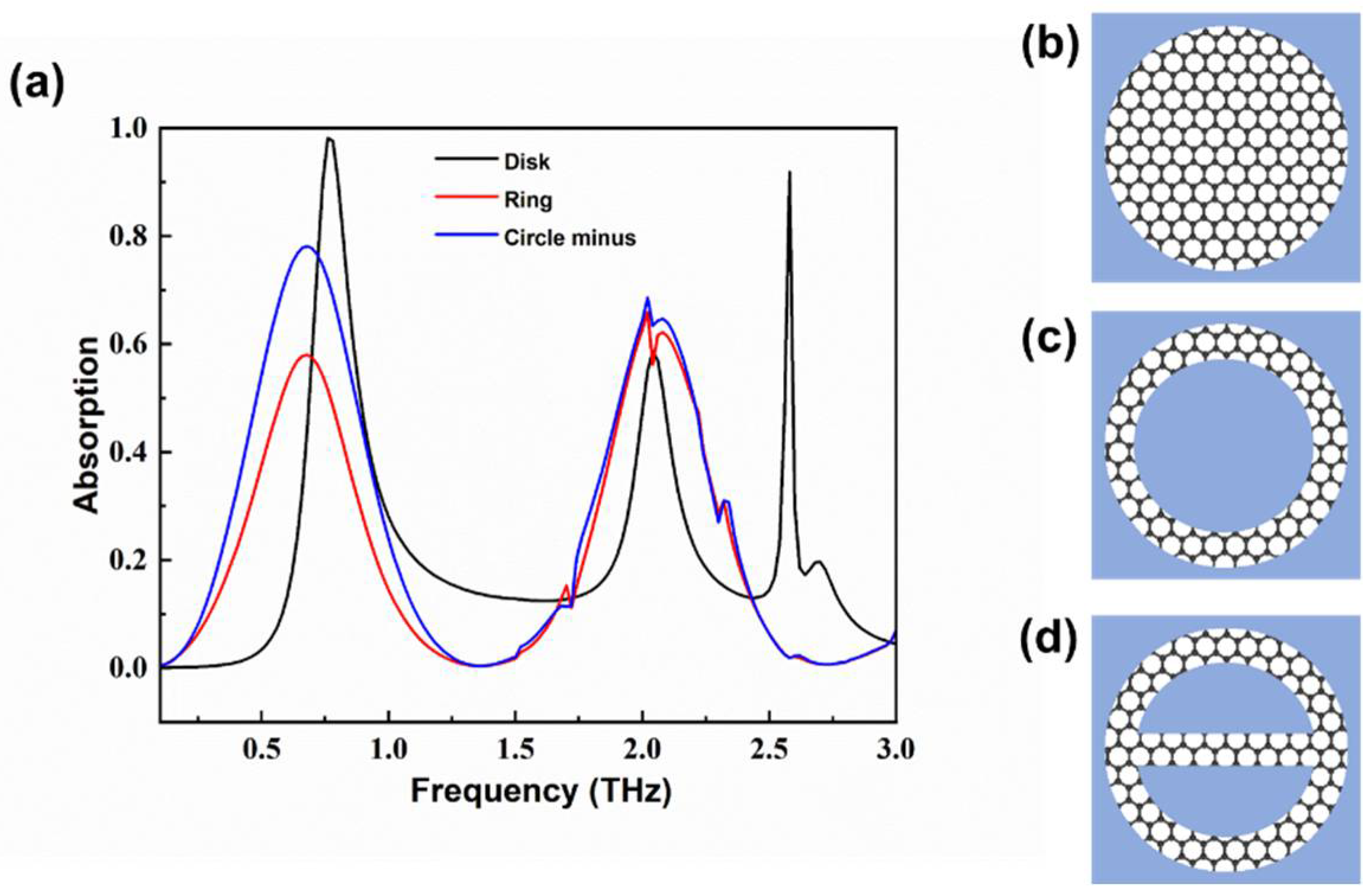
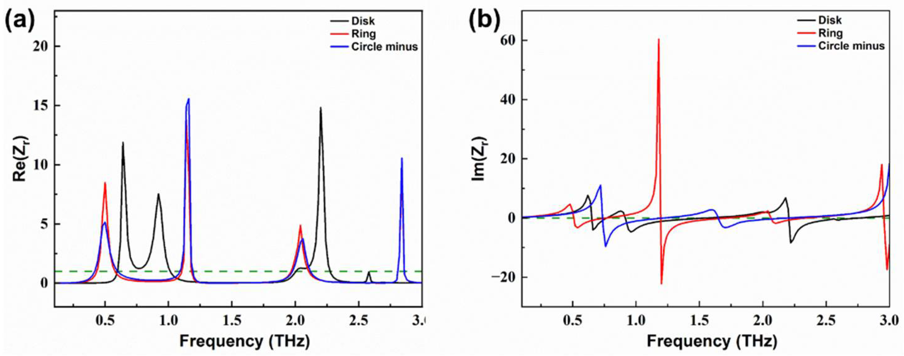
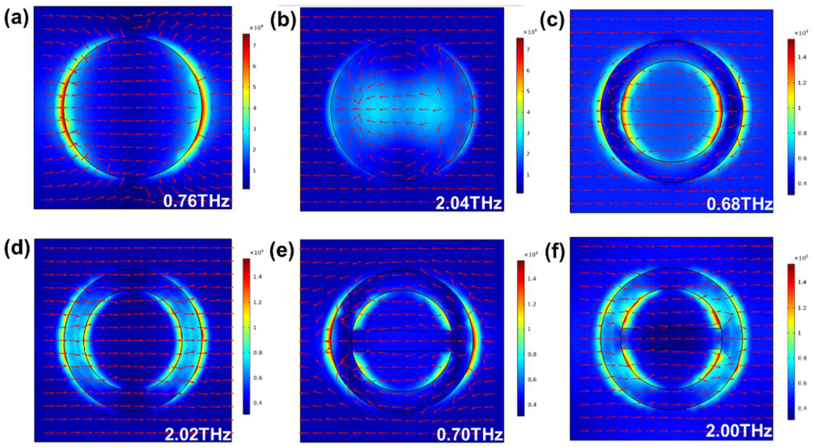
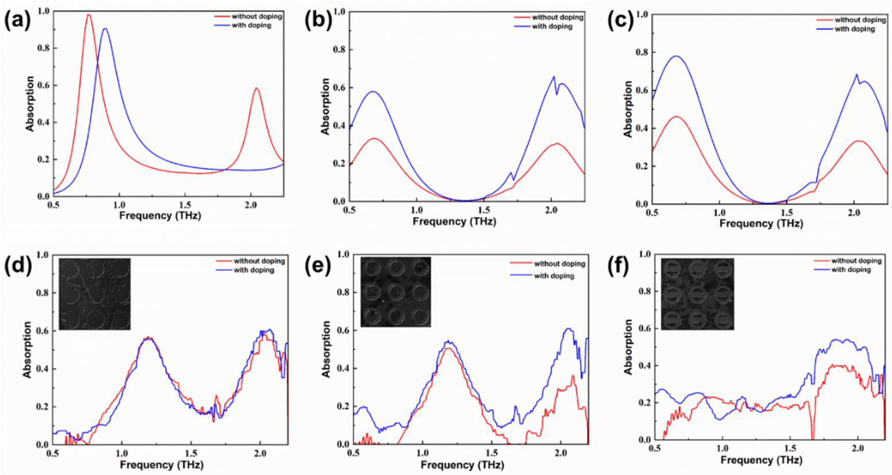
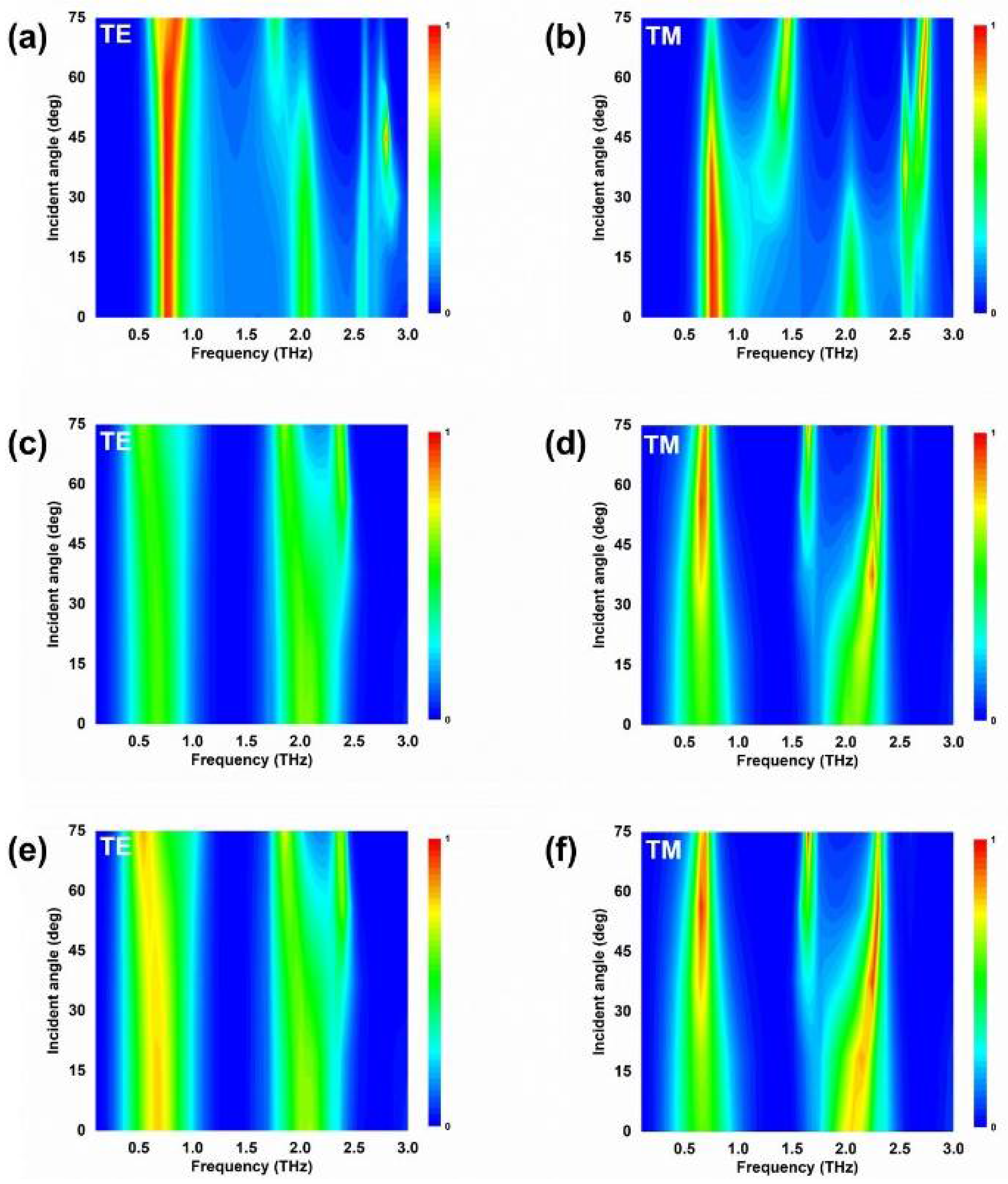
The PI and graphene film were purchased from SixCarbon Technology Shenzhen Co. Ltd (Shenzhen, China). The polydimethylsiloxane (PDMS), polymethyl methacrylate (PMMA), and oxidized wafers were provided by Suzhou Research Materials Microtech Co., Ltd. (Suzhou, China). The acetone and ferric chloride (FeCl3) solution were purchased from China National Pharmaceutical Group Co., Ltd. (Beijing, China). The graphene structures were etched by laser direct writing lithography (Microlab 100). The electromagnetic properties of the fabricated THz metamaterial absorbers were tested with the help of the 41st Institute of China Electronics Technology Group Corporation (Qingdao, China).
As shown in Figure 2, the detailed preparation steps are provided in the following section. (1) The graphene grown on copper foil is fabricated through the conventional chemical vapor deposition (CVD) method. The copper foil needs to be removed before transferring to the target substrate. Specifically, the graphene/copper film is spin-coated with a layer of polymethyl methacrylate. The PMMA/graphene/copper sample is immersed in the FeCl3 solution to dissolve the underlying copper foil. Then, the obtained graphene/PMMA is poured into the acetone to extrude PMMA. (2) A 200 nm Al film is sputter-coated onto the silicon oxide wafer to obtain a metal substrate. Then, the PI is fixed on the Al substrate after sticking a layer of PDMS film with a superior adhesion. (3) The stripped graphene is tiled on the fabricated PI/Al substrate. Then, variously patterned graphene is fabricated by laser direct writing lithography.
The THz time-domain spectrometer system was applied to measure the performance of the prepared THz metamaterial absorber (41st Institute of China Electronics Technology Group Corporation, Qingdao, China). Here, a 1560 nm femtosecond fiber laser (TOPTICA, Munich, Germany) with a pulse of 100 fs (FemtoFErb1560) was adopted to excite a signal source for THz generation. The minimum spot size of the THz-TDS systems is 1–2 mm. The incident angle is set as 12° for further THz optical absorption measurement. The behavior of the fabricated absorber is investigated by measuring the reflection of the large planar array (1 cm × 1 cm), while the transmission can be ignored due to the metal mirror.

3. Results

In order to study the absorption performance of the designed graphene-based THz metamaterial, the absorption spectra and the electronic field distribution are studied through simulations. In the simulations, the relaxation time and Fermi level are set to 1 ps and 0.3 eV, respectively. As can be seen from Figure 3a, the absorption peak of disk-patterned graphene metamaterial (Figure 3b) corresponding to the absorption values of 98.2% appears at 0.76 THz. The other two absorption peaks appear at 2.04 and 2.58 THz. In addition, the various patterns are considered to play a role in altering the absorption properties of THz metamaterial absorbers. Therefore, a ring pattern (Figure 3c) with an external radius of 35μm and an inside radius of 25 μm is chosen as the graphene layer of THz metamaterial. It is obvious that there are two absorption peaks corresponding to the absorption values of 58% and 66% at 0.68 and 2.02 THz, respectively. Meanwhile, the circled minus pattern with an extra rectangle is considered to be the surface graphene pattern of the THz metamaterial absorber to study the absorption properties, as shown in Figure 3d. The absorption curve shows that circled minus-patterned graphene metamaterial exhibits better THz wave absorption performance than ring-patterned graphene metamaterial around a similar frequency. This can be ascribed to the increase in functional graphene size.
Furthermore, the result shows that the full width of the absorption curves at half maxima of the ring-patterned graphene metamaterial and circled minus-patterned graphene metamaterial is broader than that of the full disk-patterned graphene metamaterial. This can be attributed to the impedance-matching effect, which is used to explain the physical mechanism of the absorption properties for broadband absorbers. The relative impedance can be expressed as [44]:
Z r = Z in Z 0 = ( 1 + S 11 ( ω ) ) 2 S 21 ( ω ) 2 ( 1 S 11 ( ω ) ) 2 S 21 ( ω ) 2
where Z 0 represents the free impedance and Z in is equal to the input impedance of the absorber. When the real parts are close to 1 and the imaginary parts approach 0, the designed THz metamaterial absorber can achieve perfect impedance matching. As illustrated in the real and imaginary parts of the relative impedance of the proposed THz metamaterial absorbers (Figure 4a,b), the ring-patterned graphene metamaterial and circled minus-patterned graphene metamaterials can satisfy the above condition in the frequency range of 0.58–1.1 THz, which means the impedance of ring-patterned and circled minus-patterned graphene THz metamaterials and the free space are nearly matched, while the impedance-matching band of the disk-patterned graphene metamaterial is relatively narrower.
To explore the mechanism behind the absorption performance, the electric field distribution of the top graphene layer (arrows for the direction and color for the intensity) is also investigated at the absorption peak frequencies. For the disk-shaped graphene surface, it can be noted from Figure 5a that the electric field is concentrated on the edge of the disk at a low frequency of 0.76 THz. The electric field distribution at the high frequency of 2.04 THz displayed in Figure 5b shows the field focused on the center of the disk. The physical mechanism can be explained as follows. The graphene has been demonstrated to support surface plasmon in the THz region. Surface plasmon polaritons (SPP) are perpendicularly confined evanescent electromagnetic waves, which propagate at the interface between graphene and dielectric. The propagation in the lateral direction is accompanied by the collective oscillations of surface charges, which decay exponentially in the transverse directions [45,46]. The electric distribution is applied to explore the surface plasmon resonant mode. Hence, the perfect absorption at 0.76 THz is obviously attributed to the strong coupling effect from the electric dipole resonance and bottom metal-induced current, while the absorption peak at 2.04 THz decreases with the electric dipole resonance disappearing.
Besides, the electric fields of ring-patterned graphene metamaterials, as presented in Figure 5c,d, corresponding to 0.68 and 2.02 THz, are performed to investigate the plasmonic hybridization model. Clearly, there are coupled plasmonic modes responding to absorption peaks. The dipole of the inner ring and the dipole of the outer ring jointly realize the formation of the absorption peaks.
As for circled minus-patterned graphene metamaterials, the electric field distribution depicted in Figure 5e,f indicates that a clear dipole is formed in the outer ring of the structure and a quadrupole resonance mode is formed in the inner ring. The dipolar modes interact with each other and contribute to the absorption peak at the frequency of 0.70 and 2.00 THz. Such behaviors have been proven to achieve high absorptivity, as shown in Figure 3a.
According to the Drude model, the surface conductivity of graphene mainly depends on the Fermi level, which can be adjusted by applying bias voltage or chemical doping. Compared to previous works, numerical simulation and chemical doping both are adopted to study the effect of Fermi levels on the performance of THz metamaterial absorbers in this work. First, the simulative absorption spectra of the disk pattern for the Fermi level are plotted in Figure 6a. With the Fermi level increasing, the absorptivity changed from 81% to 90% and the resonant frequency underwent blueshift at the low frequency. This can be ascribed to the wave vector of surface plasmon polaritons supporting k s p p ħ f r 2 / ( 2 α 0 E f c ) [47]. Because α 0 is the fine structure constant, the resonant frequency f r satisfies f r n E F / R . Hence, the resonant frequency underwent blueshift with the Fermi level increasing. Moreover, the fabricated THz metamaterial absorber was adulterated with chloroauric acid (HAuCl4) to change the Fermi level. The result shown in Figure 6d reveals that there is a slight increase in absorptivity in the high resonant frequency without obvious blueshift. The behaviors can be explained by the weak surface plasmon resonance at a high frequency. The low-frequency absorption peak has little variation mainly attributed to the limited Fermi energy level changed by chemical doping. When it comes to the ring-patterned and circled minus-patterned graphene layer, the apparent enhancement of performance of two absorption peaks occurs along with the increased Fermi level in the simulation, as illustrated in Figure 6b,c. Compared to the disk-patterned graphene metamaterial, there is a remarkable improvement in the absorption properties of the ring-patterned and circled minus-patterned graphene metamaterials at the high resonant frequency (Figure 6e,f) in the experiment, which enhance the Fermi level of the prepared THz metamaterial absorber through chemical doping with chloroauric acid. Analyzing the electric field distribution shows that the improvement is a superimposed effect from multiple resonance modes. However, the chemical doping can only play a slight role in changing the Fermi level of graphene, which leads to the weak change of the resonant frequency at the low resonant frequency. It can be noted that the measured absorption curve is relatively lower than the simulated results. This can be explained by the following: (1) the simulation is performed under ideal conditions, while the experiment settings include water molecules in the air and contaminated samples that have an uncertain impact on test results; (2) some paraments, such as the dielectric constants for the materials in the simulation, are based on previous works, so these might be different from the actual paraments in the experiment.
The effect of the THz wave’s incident angle on the absorption performance is also studied for the three proposed metamaterial structures. As shown in Figure 7a,b, the simulated absorption of disk-patterned graphene metamaterial for transverse electric (TE) and transverse magnetic (TM) polarizations was investigated. For disk-patterned graphene metamaterial at TE polarization, it is noted that the proposed THz metamaterial absorber sustains excellent absorption properties with the incident angle varying from 0° to 60°. As the incident angle exceeds 60°, the effective absorption band starts to get slightly broader. Nevertheless, the absorption performance is disturbed with the incident angle increasing at TM polarization. A similar change occurred with the ring-patterned and circled minus-patterned graphene metamaterials for TM polarization. It is indicated in Figure 7d,f that the absorption bandwidth narrows to some extent as the incident angle rises at a low resonant peak. As for the TE polarization, ring-patterned and circled minus-patterned graphene metamaterial absorbers with great symmetry both exhibit incident angle independence, as expressed in Figure 7c,e. In addition, slight blueshifting as shown in Figure 7e resulted from the coupling effect of multiple plasmonic modes.

4. Conclusions

In summary, tunable THz metamaterial absorbers based on various patterns of graphene are proposed and successfully fabricated in this work. The disk-patterned THz metamaterial absorber exhibits outstanding absorption performance with the value of 98.2% at 0.76 THz. Another two absorption peaks, corresponding to 58.6% and 91.9%, appear at 2.04 and 2.58 THz. For the ring-patterned THz metamaterial absorber, two absorption peaks with the values of 58% and 66% appear at 0.68 and 2.02 THz. As for the circled minus-patterned graphene metamaterial, the absorption peak with the value of 78.1% is around 0.68 THz, and an additional absorption peak with a value of 68.6% appears at 2.02 THz. The proposed patterned graphene THz metamaterial absorbers achieve multi-band absorption theoretically. Besides, improving the absorption performance by changing the Fermi level via the HAuCl4 doping method was studied in the experiment. For the ring-patterned THz metamaterial absorber, the absorption value was increased from 36.2% to 60.9% with the HAuCl4 doping. When it comes to the circled minus-patterned graphene metamaterial, the absorption value was increased from 40.6% to 54.3%. It can be inferred that HAuCl4 has a positive influence in improving the absorption performance. The corresponding enhancement of the absorption curves is demonstrated by increasing the Fermi level of graphene in the simulation. Furthermore, the proposed absorbers have been demonstrated to maintain superior stability, with the incident angle increasing from 0° to 75° at TE polarization. The proposed patterned graphene THz metamaterial absorbers have been verified in terms of their absorption performance, tunability, and incidence angle stability. Hence, this work may provide promising applications in fabricating THz devices such as switches, sensors, and tunable absorbers.

Author Contributions

Data curation, S.Z. (Siyuan Zhou); Formal analysis, Q.L., Y.N., W.F., S.H. and S.Z. (Shuai Zhang); Investigation, W.G. and X.C.; Methodology, W.G. and X.C.; Project administration, J.M. and L.T.; Writing—original draft, S.Z. (Siyuan Zhou); Writing—review & editing, S.Z. (Siyuan Zhou), K.B., L.M., W.G. and X.C. All authors have read and agreed to the published version of the manuscript.

Funding

This work is funded by the Key Research and Development Project Key Program of Shanxi Province, China (202102040201007), General project of Natural Science Foundation of Shanxi Province (Grant No. 20210302123056), Research Project Supported by Shanxi Scholarship Council of China (2020-109), National Natural Science Foundation of China Grant No. 51975541, and National Natural Science Foundation of China Grant No. 62171414.

Institutional Review Board Statement

Not applicable.

Informed Consent Statement

Not applicable.

Data Availability Statement

Not applicable.

Conflicts of Interest

The authors declare no conflict of interest.

References

  1. Wang, Q.; Gao, B.; Raglione, M.; Wang, H.; Li, B.; Toor, F.; Arnold, M.A.; Ding, H. Design, Fabrication, and Modulation of THz Bandpass Metamaterials. Laser Photonics Rev. 2019, 13, 1900071. [Google Scholar] [CrossRef]
  2. Liang, G.; Liu, T.; Wang, Q.J. Recent Developments of Terahertz Quantum Cascade Lasers. IEEE J. Sel. Top. Quantum Electron. 2017, 23, 1–18. [Google Scholar] [CrossRef]
  3. Dang, S.; Amin, O.; Shihada, B.; Alouini, M.-S. What should 6G be? Nat. Electron. 2020, 3, 20–29. [Google Scholar] [CrossRef] [Green Version]
  4. Chen, H.; Sarieddeen, H.; Ballal, T.; Wymeersch, H.; Alouini, M.-S.; Al-Naffouri, T.Y. A Tutorial on Terahertz-Band Localization for 6G Communication Systems. IEEE Commun. Surv. Tutor. 2022, 24, 1780–1815. [Google Scholar] [CrossRef]
  5. Han, C.; Wang, Y.; Li, Y.; Chen, Y.; Abbasi, N.A.; Kurner, T.F.; Molisch, A. Terahertz Wireless Channels: A Holistic Survey on Measurement, Modeling, and Analysis. IEEE Commun. Surv. Tutor. 2022, 24, 1670–1707. [Google Scholar] [CrossRef]
  6. Osborne, I. Nanowire-based THz detection. Science 2020, 368, 484–486. [Google Scholar]
  7. Shishanov, S.; Bystrov, A.; Hoare, E.G.; Stove, A.; Gashinova, M.; Cherniakov, M.; Tran, T.-Y.; Clarke, N. Height-Finding for Automotive THz Radars. IEEE Trans. Intell. Transp. Syst. 2019, 20, 1170–1180. [Google Scholar] [CrossRef]
  8. Aharon, A.; Rozban, D.; Klein, A.; Abramovich, A.; Yitzhaky, Y.; Kopeika, N.S. Detection and upconversion of three-dimensional MMW/THz images to the visible. Photonics Res. 2016, 4, 306. [Google Scholar] [CrossRef] [Green Version]
  9. Zhou, S.; Zhang, G.; Nie, Z.; Liu, H.; Yu, H.; Liu, Y.; Bi, K.; Geng, W.; Duan, H.; Chou, X. Recent advances in 3D printed structures for electromagnetic wave absorbing and shielding. Mater. Chem. Front. 2022, 6, 1736–1751. [Google Scholar] [CrossRef]
  10. Yu, P.; Besteiro, L.V.; Huang, Y.; Wu, J.; Fu, L.; Tan, H.H.; Jagadish, C.; Wiederrecht, G.P.; Govorov, A.O.; Wang, Z. Broadband Metamaterial Absorbers. Adv. Opt. Mater. 2018, 7, 1800995. [Google Scholar] [CrossRef] [Green Version]
  11. Tao, G.; Yi, Y.; Zang, M.; Zheng, Z.; Yi, Y. Simulated Performance of a Broadband Solar Absorber Composed of Sectioned Au Disk Structures and ZnS/Au Thin Layers. Coatings 2022, 12, 1863. [Google Scholar] [CrossRef]
  12. Hu, X.; Xu, G.; Wen, L.; Wang, H.; Zhao, Y.; Zhang, Y.; Cumming, D.R.S.; Chen, Q. Metamaterial absorber integrated microfluidic terahertz sensors. Laser Photonics Rev. 2016, 10, 962–969. [Google Scholar] [CrossRef] [Green Version]
  13. Wang, X.; Lin, J.; Yan, Z.; Yi, Z.; Yu, J.; Zhang, W.; Qin, F.; Wu, X.; Zhang, J.; Wu, P. Tunable high-sensitivity sensing detector based on Bulk Dirac semimetal. RSC Adv. 2022, 12, 32583–32591. [Google Scholar] [CrossRef]
  14. Zheng, Z.; Luo, Y.; Yang, H.; Yi, Z.; Zhang, J.; Song, Q.; Yang, W.; Liu, C.; Wu, X.; Wu, P. Thermal tuning of terahertz metamaterial absorber properties based on VO(2). Phys. Chem. Chem. Phys. 2022, 24, 8846–8853. [Google Scholar] [CrossRef]
  15. Tao, H.; Landy, N.I.; Bingham, C.M.; Zhang, X.; Averitt, R.D.; Padilla, W.J. A metamaterial absorber for the terahertz regime: Design, fabrication and characterization. Opt. Express 2008, 16, 7181–7188. [Google Scholar] [CrossRef] [PubMed]
  16. Chen, Z.; Zhang, Y.-X. Planar terahertz metamaterial with three-resonant frequencies. Chin. Phys. B 2013, 22, 067802. [Google Scholar] [CrossRef]
  17. Liu, X.; Zhang, Q.; Cui, X. Ultra-broadband Polarization-Independent Wide-Angle THz Absorber Based on Plasmonic Resonances in Semiconductor Square Nut-Shaped Metamaterials. Plasmonics 2016, 12, 1137–1144. [Google Scholar] [CrossRef]
  18. Kowerdziej, R.; Jaroszewicz, L. Tunable dual-band liquid crystal based near-infrared perfect metamaterial absorber with high-loss metal. Liq. Cryst. 2019, 46, 1568–1573. [Google Scholar] [CrossRef]
  19. Bendelala, F.; Cheknane, A.; Hilal, H.S. Thermally switchable meta-material absorber involving vanadium dioxide semiconductor–metal transition for thermo photovoltaic conversion. Mater. Res. Express 2018, 5, 015803. [Google Scholar] [CrossRef]
  20. Zhu, Y.W.; Murali, S.; Cai, W.W.; Li, X.S.; Suk, J.W.; Potts, J.R.; Ruoff, R.S. Graphene and Graphene Oxide: Synthesis, Properties, and Applications. Adv. Mater. 2010, 22, 3906–3924. [Google Scholar] [CrossRef]
  21. Xiang, R. Atomic precision manufacturing of carbon nanotube—A perspective. Int. J. Extrem. Manuf. 2022, 4, 023001. [Google Scholar] [CrossRef]
  22. Zhang, Y.; Feng, Y.; Jiang, T.; Cao, J.; Zhao, J.; Zhu, B. Tunable broadband polarization rotator in terahertz frequency based on graphene metamaterial. Carbon 2018, 133, 170–175. [Google Scholar] [CrossRef]
  23. Wang, Q.H.; Kalantar-Zadeh, K.; Kis, A.; Coleman, J.N.; Strano, M.S. Electronics and optoelectronics of two-dimensional transition metal dichalcogenides. Nat. Nanotechnol. 2012, 7, 699–712. [Google Scholar] [CrossRef] [PubMed]
  24. Patel, S.K.; Parmar, J.; Kosta, Y.P.; Ladumor, M.; Zakaria, R.; Nguyen, T.K.; Dhasarathan, V. Design of graphene metasurface based sensitive infrared biosensor. Sens. Actuators A Phys. 2020, 301, 111767. [Google Scholar] [CrossRef]
  25. Novoselov, K.S.; Geim, A.K.; Morozov, S.V.; Jiang, D.; Zhang, Y.; Dubonos, S.V.; Grigorieva, I.V.; Firsov, A.A. Electric field effect in atomically thin carbon films. Science 2004, 306, 666–669. [Google Scholar] [CrossRef] [PubMed] [Green Version]
  26. Grigorenko, A.N.; Polini, M.; Novoselov, K.S. Graphene plasmonics. Nat. Photonics 2012, 6, 749–758. [Google Scholar] [CrossRef]
  27. Vakil, A.; Engheta, N. Transformation Optics Using Graphene. Science 2011, 332, 1291–1294. [Google Scholar] [CrossRef] [Green Version]
  28. Chen, H.; Chen, Z.; Yang, H.; Wen, L.; Yi, Z.; Zhou, Z.; Dai, B.; Zhang, J.; Wu, X.; Wu, P. Multi-mode surface plasmon resonance absorber based on dart-type single-layer graphene. RSC Adv. 2022, 12, 7821–7829. [Google Scholar] [CrossRef]
  29. Ren, H.; Shangguan, Q.; Song, Z.; Zhao, Y.; Yi, Z.; Ma, G.; Zhang, J.; Yang, H.; Wang, S.; Wu, P. Perfect Absorption of Fan-Shaped Graphene Absorbers with Good Adjustability in the Mid-Infrared. Coatings 2022, 12, 990. [Google Scholar] [CrossRef]
  30. Ferrari, A.C. Raman spectroscopy of graphene and graphite: Disorder, electron-phonon coupling, doping and nonadiabatic effects. Solid State Commun. 2007, 143, 47–57. [Google Scholar] [CrossRef]
  31. Yu, Y.J.; Zhao, Y.; Ryu, S.; Brus, L.E.; Kim, K.S.; Kim, P. Tuning the Graphene Work Function by Electric Field Effect. Nano Lett. 2009, 9, 3430–3434. [Google Scholar] [CrossRef] [PubMed]
  32. Thomas, L.; Sorathiya, V.; Patel, S.K.; Guo, T. Graphene-based tunable near-infrared absorber. Microw. Opt. Technol. Lett. 2019, 61, 1161–1165. [Google Scholar] [CrossRef]
  33. Liu, Y.; Huang, R.; Ouyang, Z. Terahertz absorber with dynamically switchable dual-broadband based on a hybrid metamaterial with vanadium dioxide and graphene. Opt. Express 2021, 29, 20839–20850. [Google Scholar] [CrossRef] [PubMed]
  34. Galiffi, E.; Pendry, J.B.; Huidobro, P.A. Broadband Tunable THz Absorption with Singular Graphene Metasurfaces. ACS Nano 2018, 12, 1006–1013. [Google Scholar] [CrossRef] [PubMed] [Green Version]
  35. Chen, X.; Tian, Z.; Lu, Y.; Xu, Y.; Zhang, X.; Ouyang, C.; Gu, J.; Han, J.; Zhang, W. Electrically Tunable Perfect Terahertz Absorber Based on a Graphene Salisbury Screen Hybrid Metasurface. Adv. Opt. Mater. 2019, 8, 1900660. [Google Scholar] [CrossRef]
  36. Shangguan, Q.; Chen, Z.; Yang, H.; Cheng, S.; Yang, W.; Yi, Z.; Wu, X.; Wang, S.; Yi, Y.; Wu, P. Design of Ultra-Narrow Band Graphene Refractive Index Sensor. Sensors 2022, 22, 6483. [Google Scholar] [CrossRef]
  37. Wang, F.; Huang, S.; Li, L.; Chen, W.; Xie, Z. Dual-band tunable perfect metamaterial absorber based on graphene. Appl. Opt. 2018, 57, 6916–6922. [Google Scholar] [CrossRef]
  38. Xiao, B.; Gu, M.; Xiao, S. Broadband, wide-angle and tunable terahertz absorber based on cross-shaped graphene arrays. Appl. Opt. 2017, 56, 5458–5462. [Google Scholar] [CrossRef]
  39. Mou, N.; Sun, S.; Dong, H.; Dong, S.; He, Q.; Zhou, L.; Zhang, L. Hybridization-induced broadband terahertz wave absorption with graphene metasurfaces. Opt. Express 2018, 26, 11728–11736. [Google Scholar] [CrossRef] [Green Version]
  40. Qi, L.; Liu, C.; Ali Shah, S.M. A broad dual-band switchable graphene-based terahertz metamaterial absorber. Carbon 2019, 153, 179–188. [Google Scholar] [CrossRef]
  41. Luo, H.; Shangguan, Q.; Yi, Y.; Cheng, S.; Yi, Y.; Li, Z. A Tunable “Ancient Coin”-Type Perfect Absorber with High Refractive Index Sensitivity and Good Angular Polarization Tolerance. Coatings 2021, 11, 814. [Google Scholar] [CrossRef]
  42. Liu, W.; Song, Z. Terahertz absorption modulator with largely tunable bandwidth and intensity. Carbon 2021, 174, 617–624. [Google Scholar] [CrossRef]
  43. Jiang, Y.; Zhang, H.; Wang, J.; Gao, C.N.; Wang, J.; Cao, W.P. Design and performance of a terahertz absorber based on patterned graphene. Opt. Lett. 2018, 43, 4296–4299. [Google Scholar] [CrossRef] [PubMed]
  44. Fang, B.; Chen, L.; Deng, Y.; Jing, X.; Li, X. Numerical investigation of terahertz polarization-independent multiband ultrahigh refractive index metamaterial by bilayer metallic rectangular ring structure. RSC Adv. 2018, 8, 22361–22369. [Google Scholar] [CrossRef] [PubMed] [Green Version]
  45. Jablan, M.; Buljan, H.; Soljačić, M. Plasmonics in graphene at infrared frequencies. Phys. Rev. B 2009, 80, 245435. [Google Scholar] [CrossRef] [Green Version]
  46. Amin, M.; Farhat, M.; Bagci, H. An ultra-broadband multilayered graphene absorber. Opt. Express 2013, 21, 29938–29948. [Google Scholar] [CrossRef]
  47. Liu, P.; Cai, W.; Wang, L.; Zhang, X.; Xu, J. Tunable terahertz optical antennas based on graphene ring structures. Appl. Phys. Lett. 2012, 100, 153111. [Google Scholar] [CrossRef]
Figure 1. (a) Schematic of the proposed absorber based patterned graphene metamaterials. (b) Top view of unit cell.
Coatings 13 00059 g001
Figure 2. Preparation of graphene film and the proposed absorber based patterned graphene metamaterials.
Coatings 13 00059 g002
Figure 3. (a) Simulated absorption curves of proposed patterned graphene metamaterials absorbers. (b) Top view of disk-patterned graphene unit cell. (c) Top view of ring-patterned graphene unit cell. (d) Top view of circled minus-patterned graphene unit cell.
Coatings 13 00059 g003
Figure 4. (a) Real parts and (b) imaginary parts of the relative impedance of different patterns of the graphene THz metamaterials absorbers.
Coatings 13 00059 g004
Figure 5. Electric field distribution of top disk-patterned graphene of the unit cell corresponding to (a) 0.76 THz and (b) 2.04 THz. Electric field distribution of top ring-patterned graphene of the unit cell corresponding to (c) 0.68 THz and (d) 2.02 THz. Electric field distribution of top circled minus-patterned graphene of the unit cell corresponding to (e) 0.70 THz and (f) 2.00 THz.
Coatings 13 00059 g005
Figure 6. Simulated absorption spectra before and after doping process for (a) disk pattern, (b) ring pattern, and (c) circled minus pattern. Tested absorption spectra of undoped absorbers and doped absorbers for (d) disk pattern, (e) ring pattern, and (f) circled minus pattern with the optical image in the upper left corner.
Coatings 13 00059 g006
Figure 7. The absorption spectra of the designed disk-patterned graphene THz metamaterial absorber with different incident angle for (a) TE polarization and (b) TM polarization. The absorption spectra of the designed ring-patterned graphene THz metamaterial absorber with different incident angle for (c) TE polarization and (d) TM polarization. The absorption spectra of the designed circled minus-patterned graphene THz metamaterial absorber with different incident angle for (e) TE polarization and (f) TM polarization.
Coatings 13 00059 g007
Table 1. Nomenclature table of abbreviations and parameters for the proposed absorber.
SymbolDefinitionUnit
Rradius of disk-patterned arrayμm
Pthe length of periodic unit μm
σ gra surface conductivity of grapheneS/m
σ intra intraband conductivityS/m
σ inter interband conductivityS/m
ω frequencyTHz
τ relaxation timeps
E f Fermi leveleV
T absolute temperatureK
k B Boltzmann constantJ/K
e electron chargeC
ħ reduced Plank constantJ·s
Disclaimer/Publisher’s Note: The statements, opinions and data contained in all publications are solely those of the individual author(s) and contributor(s) and not of MDPI and/or the editor(s). MDPI and/or the editor(s) disclaim responsibility for any injury to people or property resulting from any ideas, methods, instructions or products referred to in the content.

