
A Review on Sustainable Manufacturing of Ceramic-Based Thin Films by Chemical Vapor Deposition (CVD): Reactions Kinetics and the Deposition Mechanisms
 , , and
Abstract
:1. Introduction
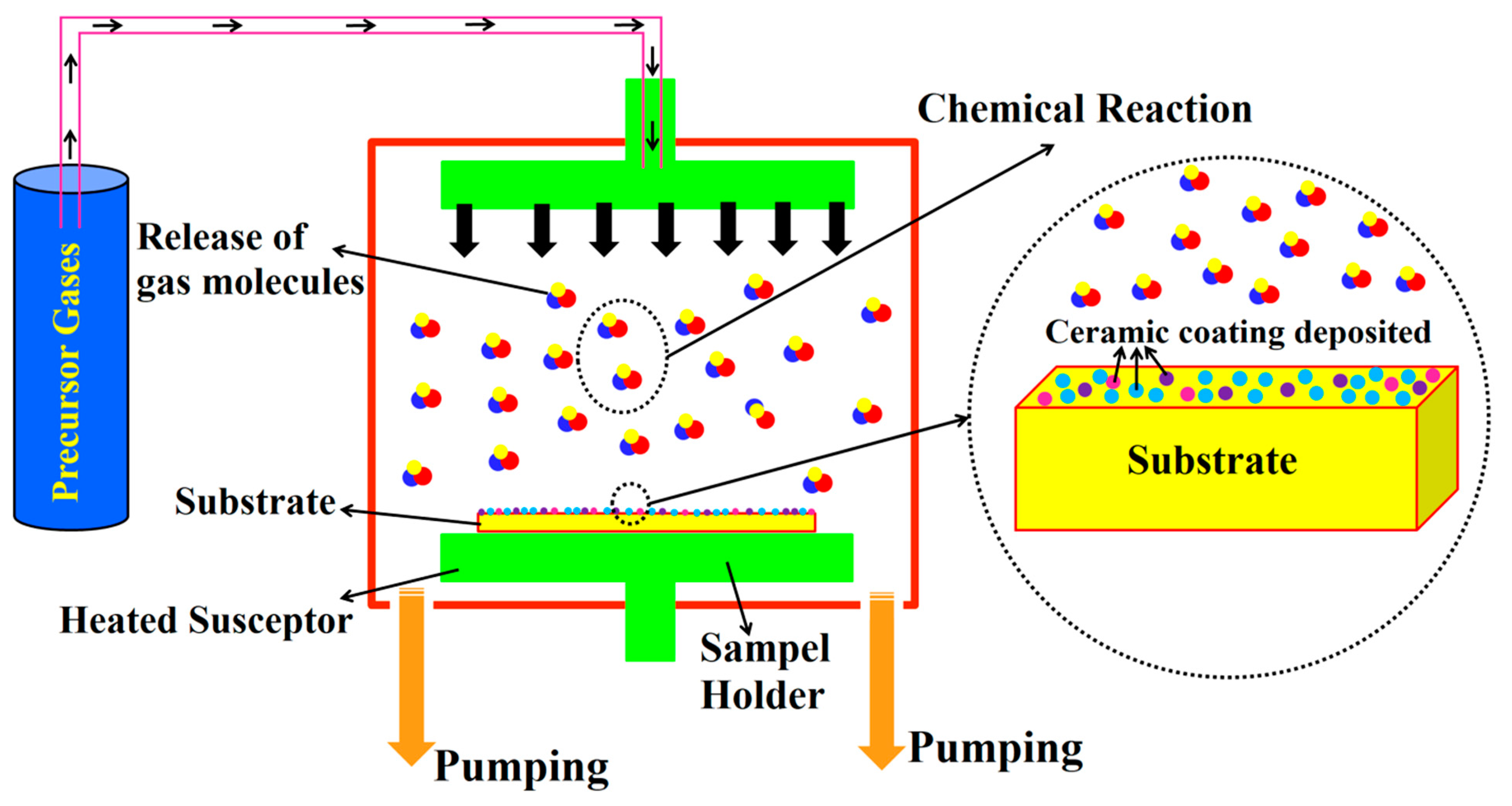
2. Principles of the CVD Process
- (a)
- Decomposition of reactive gases.
- (b)
- Gas combination.
- (c)
- Gas hydrolysis.
- (d)
- Gas oxidation.
- (e)
- Reduction of some gases.
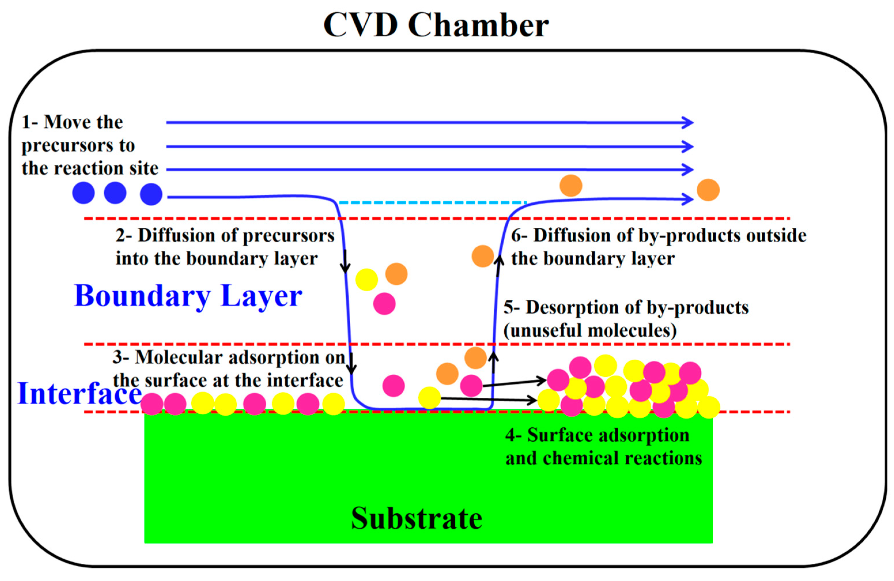
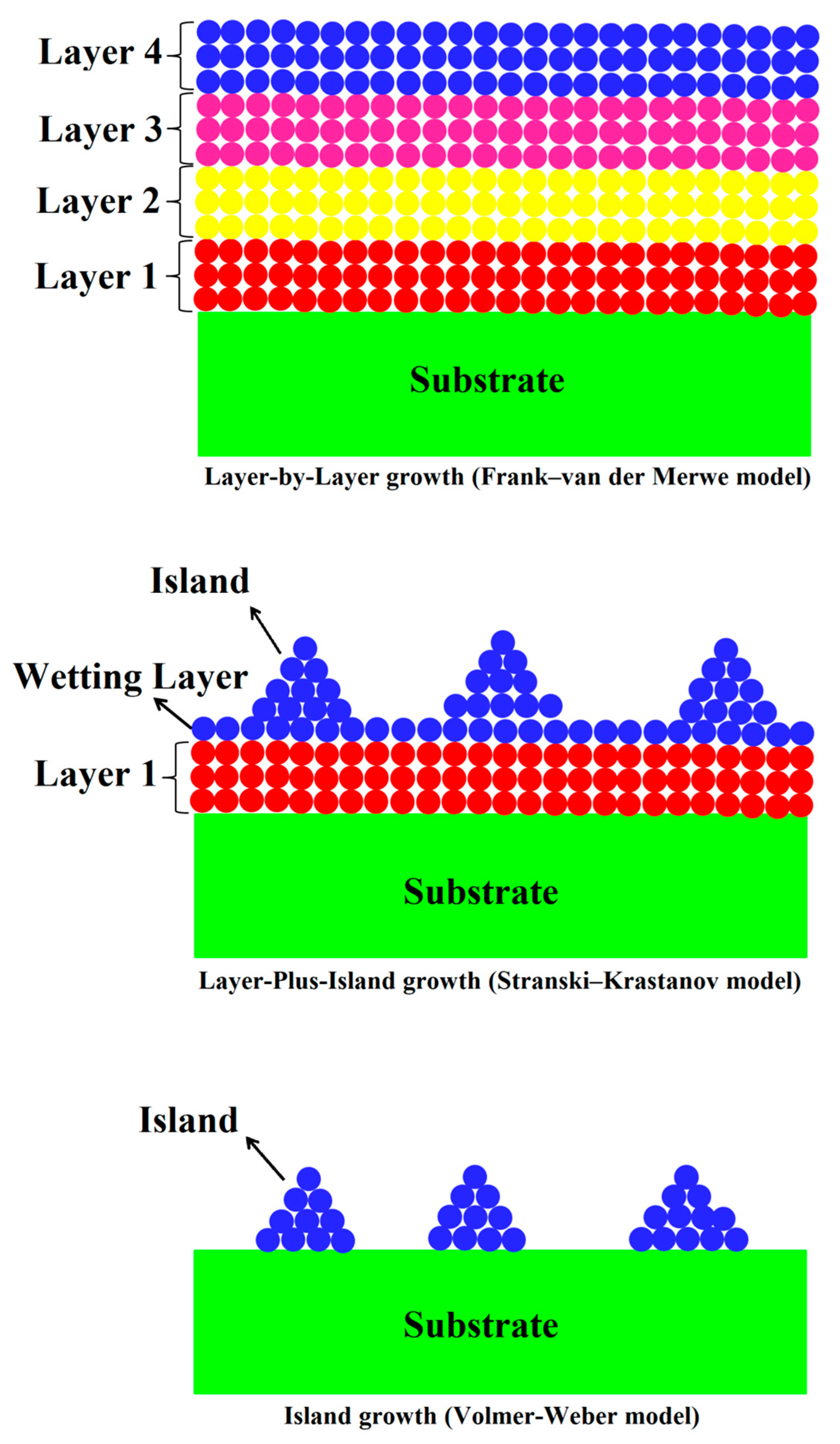
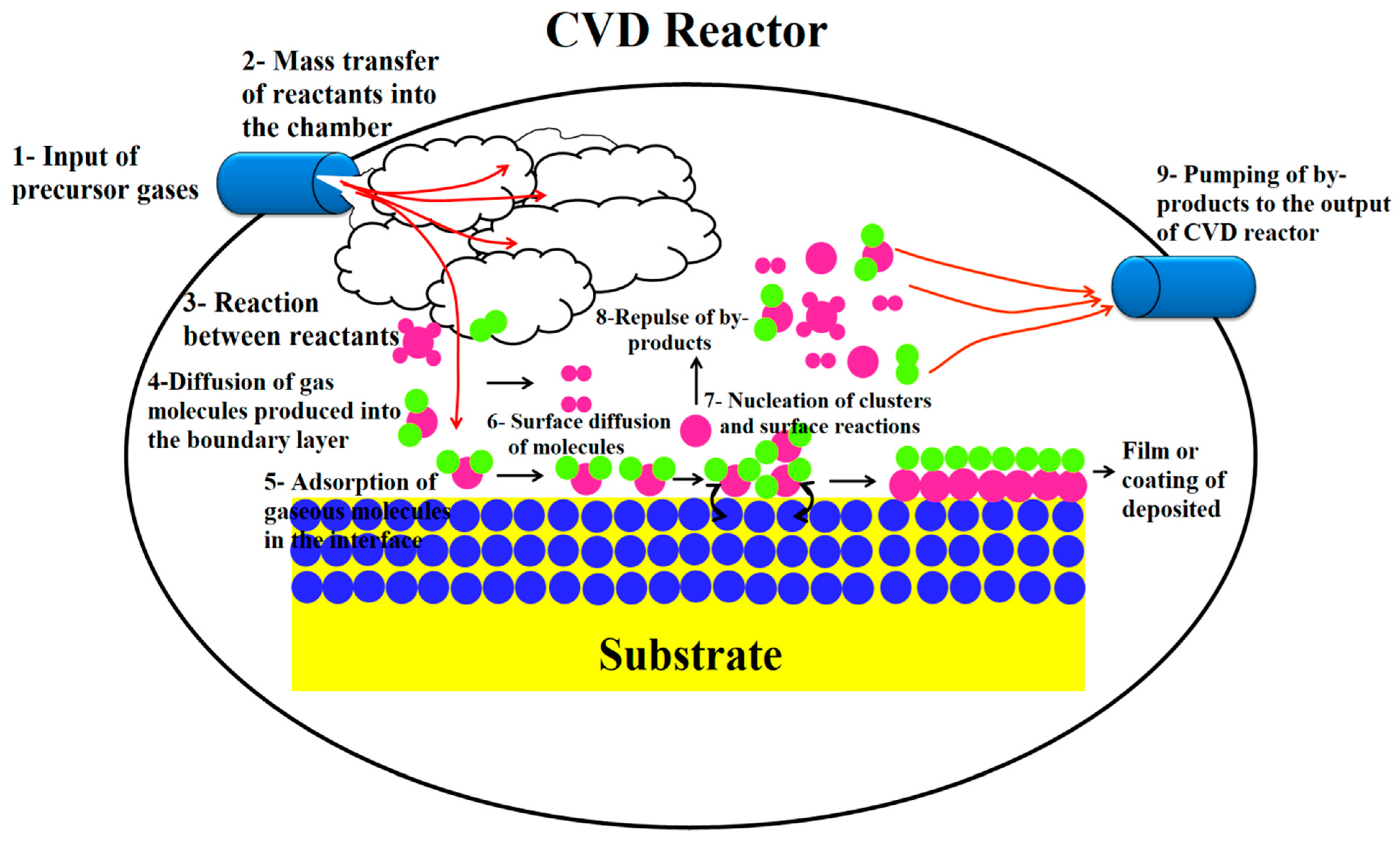
3. Deposition Mechanism in the CVD Process
- (a)
- Heat transfer and diffusion of the reactants from the gas reservoir to the reaction zone.
- (b)
- Occurrence of chemical reactions in the gas phase to produce reactive samples and byproducts.
- (c)
- Transfer of primary reactants and their products onto the metallic or nonmetallic substrate.
- (d)
- Chemical adsorption and the diffusion of these products on the metallic or nonmetallic substrate.
- (e)
- Inhomogeneous reactions by the surface resulting in the formation of ceramic nanocomposite coatings on the metallic or nonmetallic substrate.
- (f)
- Heat transfer and outflow of the by-products outside the reaction chamber (deposition layer zone).
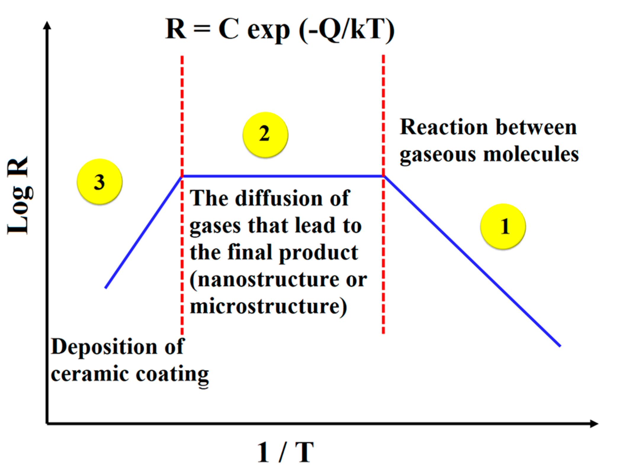
4. Kinetics of Reactions and Coating Production in the CVD Process
5. Summary
Author Contributions
Funding
Institutional Review Board Statement
Informed Consent Statement
Data Availability Statement
Conflicts of Interest
References
- Hallad, S.A.; Banapurmath, N.R.; Hunashyal, A.M.; Shettar, A.S. Study of the effect of nanocomposite thin film coating on cutting tool tip for tribological applications. Mater. Today Proc. 2020, 27, 37–39. [Google Scholar] [CrossRef]
- Sabzi, M.; Mousavi Anijdan, S.H.; Asadian, M. The effect of substrate temperature on microstructural evolution and hardenability of tungsten carbide coating in hot filament chemical vapor deposition. Int. J. Appl. Ceram. Technol. 2018, 15, 1350–1357. [Google Scholar] [CrossRef]
- Perez-Mariano, J.; Lau K, H.; Alvarez, E.; Malhotra, R. Coatings for corrosion protection of porous substrates in gasifier components, Surf. Coat. Technol. 2008, 202, 2794–2800. [Google Scholar] [CrossRef]
- Delfini, A.; Vricella, A.; Bueno Morles, R.; Pastore, R.; Micheli, D.; Gugliermetti, F.; Marchetti, M. CVD nano-coating of carbon composites for space materials atomic oxygen shielding. Procedia Struct. Integr. 2017, 3, 208–216. [Google Scholar] [CrossRef]
- Li, Z.; Wang, Y.; Xiong, X.; Li, X.; Chen, Z.; Sun, W. Microstructure and growth behavior of Hf (Ta)C ceramic coating synthesized by low pressure chemical vapor deposition. J. Alloys Compd. 2017, 705, 79–88. [Google Scholar] [CrossRef]
- Mousavi Anijdan, S.H.; Sabzi, M.; Asadian, M.; Jafarian, H.R. Effect of sub-layer temperature during HFCVD process on morphology and corrosion behavior of tungsten carbide coating. Int. J. Appl. Ceram. Technol. 2019, 16, 243–253. [Google Scholar] [CrossRef] [Green Version]
- Strauss, H.W.; Chromik, R.R.; Hassani, S.; Klemberg-Sapieha, J.E. In situ tribology of nanocomposite Ti–Si–C–H coatings prepared by PE-CVD. Wear 2011, 272, 133–148. [Google Scholar] [CrossRef]
- Feng, B.; Cao, D.M.; Meng, W.J.; Rehn, L.E.; Baldo, P.M.; Doll, G.L. Probing for mechanical and tribological anomalies in the TiC/amorphous hydrocarbon nanocomposite coating system. Thin Solid Film. 2001, 398–399, 210–216. [Google Scholar] [CrossRef]
- Stueber, M.; Albers, U.; Leiste, H.; Ulrich, S.; Holleck, H.; Barna, P.B.; Kovacs, A.; Hovsepian, P.; Gee, I. Multifunctional nanolaminated PVD coatings in the system Ti–Al–N–C by combination of metastable fcc phases and nanocomposite microstructures. Surf. Coat. Technol. 2006, 200, 6162–6171. [Google Scholar] [CrossRef]
- Tamilarasan, T.R.; Rajendran, R.; Rajagopal, G.; Sudagar, J. Effect of surfactants on the coating properties and corrosion behaviour of Ni–P–nano-TiO2 coatings. Surf. Coat. Technol. 2015, 276, 320–326. [Google Scholar] [CrossRef]
- Sabzi, M.; Mersagh Dezfuli, S. Deposition of Al2O3 ceramic film on copper-based heterostructured coatings by aluminizing process: Study of the electrochemical responses and corrosion mechanism of the coating. Int. J. Appl. Ceram. Technol. 2019, 16, 195–210. [Google Scholar] [CrossRef] [Green Version]
- Shahriari, A.; Aghajani, H. Electrophoretic deposition of 3YSZ coating on AZ91D using an aluminum interlayer. Prot. Met. Phys. Chem. Surf. 2017, 53, 518–526. [Google Scholar] [CrossRef]
- Wang, J.B.; Ren, Z.; Hou, Y.; Yan, X.L.; Liu, P.Z.; Zhang, H.; Zhang, H.X.; Guo, J.J. A review of graphene synthesis at low temperatures by CVD methods. New Carbon Mater. 2020, 35, 193–208. [Google Scholar] [CrossRef]
- Pammi, S.V.N.; Maddaka, R.; Tran, V.-D.; Eom, J.-H.; Pecunia, V.; Majumder, S.; Kim, M.-D.; Yoon, S.G. CVD-deposited hybrid lead halide perovskite films for high-responsivity, self-powered photodetectors with enhanced photo stability under ambient conditions. Nano Energy 2020, 74, 104872. [Google Scholar] [CrossRef]
- Shahriari, A.; Aghajani, H. Electrophoretic Deposition of 3YSZ Coating on AZ91D Alloy Using Al and Ni-P Interlayers. J. Mater. Eng. Perform. 2016, 25, 4369–4382. [Google Scholar] [CrossRef]
- Pedersen, H.; Barry, S.T.; Sundqvist, J. Green CVD—Toward a sustainable philosophy for thin film deposition by chemical vapor deposition. J. Vac. Sci. Technol. A 2021, 39, 051001. [Google Scholar] [CrossRef]
- Hong, Y.L.; Liu, Z.; Wang, L.; Zhou, T.; Ma, W.; Xu, C.; Feng, S.; Chen, L.; Chen, M.L.; Sun, D.M.; et al. Chemical vapor deposition of layered two-dimensional MoSi2N4 materials. Science 2020, 369, 670–674. [Google Scholar] [CrossRef]
- Alagh, A.; Annanouch, F.E.; Umek, P.; Bittencourt, C.; Sierra-Castillo, A.; Haye, E.; FrançoisColomer, J.; Llobet, E. CVD growth of self-assembled 2D and 1D WS2 nanomaterials for the ultrasensitive detection of NO2. Sens. Actuators B Chem. 2021, 326, 128813. [Google Scholar] [CrossRef]
- Tamilarasan, T.R.; Sanjith, U.; Rajendran, R.; Rajagopal, G.; Sudagar, J. Effect of Reduced Graphene Oxide Reinforcement on the Wear Characteristics of Electroless Ni-P Coatings. J. Mater. Eng. Perform. 2018, 27, 3044–3053. [Google Scholar] [CrossRef]
- Tang, L.; Li, T.; Luo, Y.; Feng, S.; Cai, Z.; Zhang, H.; Liu, B.; Cheng, H.M. Vertical Chemical Vapor Deposition Growth of Highly Uniform 2D Transition Metal Dichalcogenides. ACS Nano 2020, 14, 4646–4653. [Google Scholar] [CrossRef]
- Raiford, J.A.; Oyakhire, S.T.; Bent, S.F. Applications of atomic layer deposition and chemical vapor deposition for perovskite solar cells. Energy Environ. Sci. 2020, 13, 1997–2023. [Google Scholar] [CrossRef]
- Paradisanos, I.; Shree, S.; George, A.; Leisgang, N.; Robert, C.; Watanabe, K.; Taniguchi, T.; Warburton, R.J.; Turchanin, A.; Marie, X.; et al. Controlling interlayer excitons in MoS2 layers grown by chemical vapor deposition. Nat. Commun. 2020, 11, 2391. [Google Scholar] [CrossRef] [PubMed]
- Li, G.; Yin, S.; Tan, C.; Chen, L.; Yu, M.; Li, L.; Yan, F. Fast Photothermoelectric Response in CVD-Grown PdSe2 Photodetectors with In-Plane Anisotropy. Adv. Funct. Mater. 2021, 31, 2104787. [Google Scholar] [CrossRef]
- Zhang, J.; Wang, F.; Shenoy, V.B.; Tang, M.; Lou, J. Towards controlled synthesis of 2D crystals by chemical vapor deposition (CVD). Mater. Today 2020, 40, 132–139. [Google Scholar] [CrossRef]
- Sabzi, M.; Mousavi Anijdan, S.H. Microstructural Analysis and Optical Properties Evaluation of Sol-Gel NiO-TiO2 Heterostructured Films used for Solar Panels. Ceram. Int. 2019, 45, 3250–3255. [Google Scholar] [CrossRef]
- Zhang, P.; Zhang, Y.; Chen, G.; Gai, W.; Kong, J. High-temperature oxidation behavior of CVD-SiC ceramic coating in wet oxygen and structural evolution of oxidation product: Experiment and first-principle calculations. Appl. Surf. Sci. 2021, 556, 149808. [Google Scholar] [CrossRef]
- Tong, M.; Fu, Q.; Liang, M.; Feng, T.; Hou, W.; Sun, J.; Shi, X. Effect of PyC-SiC double-layer interface on ablation behaviour of impacted CVD-SiCnws/HfC coating. Corr. Sci. 2021, 191, 109741. [Google Scholar] [CrossRef]
- Kong, J.; Zhang, Y.; Gai, W.; Wang, H.; Chen, G.; Zhang, P.; Li, H. Influence of crystallite morphology on the ablative behaviors of CVD-TaC coatings prepared on C/C composites beyond 2100 °C. Corr. Sci. 2022, 205, 110426. [Google Scholar] [CrossRef]
- Zhang, J.; Zhang, Y.; Chen, R.; Zhu, X.; Fu, Y. Effect of microstructure on the ablation behavior and mechanical properties of CVD-HfC coating. Corr. Sci. 2021, 192, 109815. [Google Scholar] [CrossRef]
- Baux, A.; Jacques, S.; Allemand, A.; Vignoles, G.L.; David, P.; Piquero, T.; Stempin, M.-P.; Chollon, G. Complex geometry macroporous SiC ceramics obtained by 3D-printing, polymer impregnation and pyrolysis (PIP) and chemical vapor deposition (CVD). J. Eur. Ceram. Soc. 2021, 41, 3274–3284. [Google Scholar] [CrossRef]
- Honda, Y.; Mikami, Y.; Inoue, M.; Shinag, K.; Abe, T. Low-temperature SiO2 film coatings onto Cu particles using the polygonal barrel-plasma chemical vapor deposition method. Appl. Surf. Sci. 2022, 588, 152646. [Google Scholar] [CrossRef]
- Fu, J.; Sun, Y.; Ji, Y.; Zhang, J. Fabrication of robust ceramic based superhydrophobic coating on aluminum substrate via plasma electrolytic oxidation and chemical vapor deposition methods. J. Mater. Process. Technol. 2022, 306, 117641. [Google Scholar] [CrossRef]
- Tong, M.; Fu, Q.; Hu, D.; Zhou, L.; Feng, T. Improvement of ablation resistance of CVD-HfC/SiC coating on hemisphere shaped C/C composites by introducing diffusion interface. J. Eur. Ceram. Soc. 2021, 41, 4067–4075. [Google Scholar] [CrossRef]
- Mallick, R.; Kumar, R.; Panda, A.; Sahoo, A.K. Hard turning performance evaluation using CVD and PVD coated carbide tools: A comparative study. Surf. Rev. Lett. 2022, 29, 2250020. [Google Scholar] [CrossRef]
- Zhang, J.; Zhang, Y.; Fu, Y.; Zhang, Y.; Zhu, X. Growth mechanism and ablation behavior of CVD-HfC coating on the surface of C/C composites and CVD-SiC coating. Corr. Sci. 2021, 192, 109819. [Google Scholar] [CrossRef]
- Li, B.; Li, H.; Yao, X.; Zhu, X.; Liu, N. Preparation and ablation resistance of ZrC nanowires-reinforced CVD-ZrC coating on sharp leading edge C/C composites. Appl. Surf. Sci. 2022, 584, 152617. [Google Scholar] [CrossRef]
- Wang, C. Fabrication of porous SiC nanostructured coatings on C/C composite by laser chemical vapor deposition for improving the thermal shock resistance. Ceram. Int. 2022, 48, 12450–12459. [Google Scholar] [CrossRef]
- Zheng, X.; Liu, Y.; Cao, Y.; Wang, J.; Zhang, Y. CVD synthesis of nanometer SiC coating on diamond particles. Ceram. Int. 2021, 47, 16162–16169. [Google Scholar] [CrossRef]
- Zhang, Y.; Yu, L.; Fu, T.; Wang, J.; Shen, F.; Cui, K. Microstructure evolution and growth mechanism of Si-MoSi2 composite coatings on TZM (Mo-0.5Ti-0.1Zr-0.02 C) alloy. J. Alloys Compd. 2022, 894, 162403. [Google Scholar] [CrossRef]
- Guo, Z.; Guo, B.; Zhao, Q.; Liu, W.; Zheng, Q. Optimisation of spray-mist-assisted laser machining of micro-structures on CVD diamond coating surfaces. Ceram. Int. 2021, 47, 22108–22120. [Google Scholar] [CrossRef]
- Pardo, A.; Gómez-Aleixandre, C.; Celis, J.P.; Buijnsters, J.G. Friction and wear behavior of plasma assisted chemical vapor deposited nanocomposites made of metal nanoparticles embedded in a hydrogenated amorphous carbon matrix. Surf. Coat. Technol. 2012, 206, 3116–3124. [Google Scholar] [CrossRef]
- Tynyshtykbayev, K.B.; Ainabayev, A.; Kononenko, O.; Chichkov, M.; Ramazanova, Z.; Zulkharnai, R.; Roshchupkin, D.; Sorokupudov, J.; Starkov, V.; Insepov, Z. Low temperature synthesis of graphene nanocomposites using surface passivation of porous silicon nanocrystallites with carbon atoms. Diam. Relat. Mater. 2019, 92, 53–60. [Google Scholar] [CrossRef]
- Perez-Mariano, J.; Caro, J.; Colominas, C. TiN/SiNx submicronic multilayer coatings obtained by chemical vapor deposition in a fluidized bed reactor at atmospheric pressure (AP/FBR-CVD). Surf. Coat. Technol. 2006, 201, 4021–4025. [Google Scholar] [CrossRef]
- Bobzin, K. High-performance coatings for cutting tools. CIRP J. Manuf. Sci. Technol. 2017, 18, 1–9. [Google Scholar] [CrossRef]
- Jang, J.; Kang, I.; Yi, K.W.; Cho, Y.W. Highly conducting fibrous carbon-coated silicon alloy anode for lithium ion batteries. Appl. Surf. Sci. 2018, 454, 277–283. [Google Scholar] [CrossRef]
- Meng, W.J.; Zhang, X.D.; Shi, B.; Jiang, J.C.; Rehn, L.E.; Baldo, P.M.; Tittsworth, R.C. Structure and mechanical properties of Ti–Si–N ceramic nanocomposite coatings. Surf. Coat. Technol. 2003, 163–164, 251–259. [Google Scholar] [CrossRef]
- Leem, M.; Lee, H.; Park, T.; Ahn, W.; Kim, H.; Lee, E.; Kim, H. Intriguing morphological evolution during chemical vapor deposition of HfS2 using HfCl4 and S on sapphire substrate. Appl. Surf. Sci. 2020, 509, 144701. [Google Scholar] [CrossRef]
- Hoyos-Palacio, L.M.; Paola Cuesta Castro, D.; Cristina Ortiz-Trujillo, I.; Elena Botero Palacio, L.; Janeth Galeano Upegui, B.; Javier Escobar Mora, N.; Antonio Carlos Cornelio, J. Compounds of carbon nanotubes decorated with silver nanoparticles via in-situ by chemical vapor deposition (CVD). J. Mater. Res. Technol. 2019, 8, 5893–5898. [Google Scholar] [CrossRef]
- Sevgili, E.; Karaman, M. Initiated chemical vapor deposition of poly(Hydroxypropyl methacrylate) thin films. Thin Solid Film. 2019, 687, 137446. [Google Scholar] [CrossRef]
- Méndez-Lozano, N.; Apátiga-Castro, M.; Manzano-Ramírez, A.; Rivera-Muñoz, E.M.; Velázquez-Castillo, R.; Alberto-González, C.; Zamora-Antuñano, M. Morphological study of TiO2 thin films doped with cobalt by Metal Organic Chemical Vapor Deposition. Results Phys. 2020, 16, 1–5. [Google Scholar] [CrossRef]
- Wang, M.; Jia, L.; Xu, H.; Li, A.; Peng, Y.; Tang, Z. Influence of pressure on chemical vapor deposition of boron nitride from BCl3/NH3/H2 gas mixtures. Ceram. Int. 2020, 46, 4843–4849. [Google Scholar] [CrossRef]
- Feng, X.; Jiang, L.; Li, D.; Tian, S.; Zhu, X.; Wang, H.; He, C.; Li, K. Progress and key challenges in catalytic combustion of lean methane. J. Energy Chem. 2022, 75, 173–215. [Google Scholar] [CrossRef]
- Zhang, Z.; Yang, F.; Zhang, H.; Zhang, T.; Wang, H.; Xu, Y.; Ma, Q. Influence of CeO2 addition on forming quality and microstructure of TiCx-reinforced CrTi4-based laser cladding composite coating. Mater. Charact. 2021, 171, 110732. [Google Scholar] [CrossRef]
- Morali, U.; Demiral, H.; Sensoz, S. Synthesis of carbon molecular sieve for carbon dioxide adsorption: Chemical vapor deposition combined with Taguchi design of experiment method. Powder Technol. 2019, 355, 716–726. [Google Scholar] [CrossRef]
- Zhao, Y.; Song, B.; Cui, X.; Ren, Y.; Yu, W.; Wang, Y. High electrocatalytic reduction using ZnS micropolyhedron: Direct sulfuration of ZIF-8 film on conducting glass by chemical vapour deposition. Mater. Lett. 2019, 250, 193–196. [Google Scholar] [CrossRef]
- Lee, S.; Park, W.K.; Yoon, Y.; Baek, B.; Yoo, J.S.; Kwon, S.B.; Kim, D.H.; Joon, Y.; Bong, H.; Kang, K.; et al. Quality improvement of fast-synthesized graphene films by rapid thermal chemical vapor deposition for mass production. Mater. Sci. Eng. B 2019, 242, 63–68. [Google Scholar] [CrossRef]
- Matsumura, H. Current Status of Catalytic Chemical Vapor Deposition Technology—History of Research and Current Status of Industrial Implementation. Thin Solid Film. 2019, 679, 42–48. [Google Scholar] [CrossRef]
- Zhang, S.; Wang, J.; Lu, Y.; Hou, W.; Cao, K.; Guo, S.; Wang, Z.; Wang, L. Highly ordered arrays and characterization of WS2 flakes grown by low pressure chemical vapour deposition. Chem. Phys. 2019, 523, 106–109. [Google Scholar] [CrossRef]
- Zou, C.; Li, B.; Liu, K.; Yang, X.; Li, D. Microstructure and mechanical properties of Si3N4f/BN composites with BN interphase prepared by chemical vapor deposition of borazine. J. Eur. Ceram. Soc. 2020, 40, 1139–1148. [Google Scholar] [CrossRef]
- Katamune, Y.; Arikaw, D.; Mori, D.; Izumi, A. Formation of phosphorus-incorporated diamond films by hot-filament chemical vapor deposition using organic phosphorus solutions. Thin Solid Film. 2019, 677, 28–32. [Google Scholar] [CrossRef]
- Madaka, R.; Kumari, J.; Kanneboina, V.; Jha, S.H.; Agarwal, P. Role of chamber pressure on crystallinity and composition of silicon films using silane and methane as precursors in hot-wire chemical vapour deposition technique. Thin Solid Film. 2019, 682, 126–130. [Google Scholar] [CrossRef]
- Liu, Q.; Liu, J.; Luan, X. Preparation of ZrC-SiC composite coatings by chemical vapor deposition and study of co-deposition mechanism. J. Mater. Sci. Technol. 2019, 35, 2942–2949. [Google Scholar] [CrossRef]
- Tarazona, A.; Bucio, T.D.; Oo, S.Z.; Petra, R.; Khokhar, A.Z.; Boden, S.A.; Gardes, F.Y.; Reed, G.T.; Chong, H.M. Hot wire chemical vapor deposition for silicon photonics: An emerging industrial application opportunity. Thin Solid Film. 2019, 676, 26–30. [Google Scholar] [CrossRef]
- Luo, J.; Wang, J.; Xia, F.; Huang, X. Direct growth of large area uniform double layer graphene films on MgO(100) substrates by chemical vapor deposition. Mater. Chem. Phys. 2019, 233, 213–219. [Google Scholar] [CrossRef]
- Chuang, C.; Mineharu, M.; Matsunag, M.; Liu, C.W.; Wu, B.Y.; Kenj, J.H.; Taniguchi, T.; Liang, C.T.; Aoki, N. Conductance interference effects in an electron-beam-resist-free chemical vapor deposition graphene device sandwiched between two h-BN sheets. Carbon 2019, 154, 238–243. [Google Scholar] [CrossRef]
- Basak, S.; Afzaal, M.; Yates, H.M. Optically tuned and large-grained bromine doped CH3NH3PbI3 perovskite thin films via aerosol-assisted chemical vapour deposition. Mater. Chem. Phys. 2019, 223, 157–163. [Google Scholar] [CrossRef] [Green Version]
- Silverio, V.; Canane, P.A.G.; Cardoso, S. Surface wettability and stability of chemically modified silicon, glass and polymeric surfaces via room temperature chemical vapor deposition. Colloids Surf. A Physicochem. Eng. Asp. 2019, 570, 210–217. [Google Scholar] [CrossRef]
- Dong, H.; Duan, A.; Zhong, S.; Zhang, Y.; Zhou, X. Chemical vapor deposition growth of broadband tunable light absorption and anti-reflection properties of VS2 nanostructure films. Mater. Lett. 2019, 252, 227–230. [Google Scholar] [CrossRef]
- Huang, Y. Modeling and analysis of SiO2 deposition during high-purity fused silica glass synthesis by SiCl4 chemical vapor deposition. Ceram. Int. 2019, 45, 10740–10745. [Google Scholar] [CrossRef]
- Wang, Z.; Yue, H.Y.; Yu, Z.M.; Huang, Z.; Gao, X.; Wang, B.; Song, S.S.; Guan, E.H.; Wang, W.Q.; Zhang, H.J. A novel 3D porous graphene foam prepared by chemical vapor deposition using nickel nanoparticles: Electrochemical determination of levodopa in the presence of uric acid. Microchem. J. 2019, 147, 163–169. [Google Scholar] [CrossRef]
- Liu, X.F.; Yan, G.G.; Shen, Z.W.; Wen, Z.X.; Chen, J.; He, Y.W.; Zhao, W.S.; Wang, L.; Guan, M.; Zhang, F. Homoepitaxial growth of multiple 4H-SiC wafers assembled in a simple holder via conventional chemical vapor deposition. J. Cryst. Growth 2019, 507, 283–287. [Google Scholar] [CrossRef]
- Gutiérrez-García, C.J.; Madaí Ambriz-Torres, J.; Jesús Contreras-Navarrete, J.; Gabriel Granados-Martínez, F.; Litzajaya García-Ruiz, D.; García-González, L.; Zamora-Peredo, L.; Fernando Ortega-Varela, L.; Richaud, A.; Méndez, F.; et al. Synthesis of carbon spheres by atmospheric pressure chemical vapor deposition from a serial of aromatic hydrocarbon precursors. Phys. E Low-Dimens. Syst. Nanostruct. 2019, 112, 78–85. [Google Scholar] [CrossRef]
- Arzaee, N.A.; Noh, M.F.; Aadenan, A.; Mumthas, I.N.; Ab Hamid, F.F.; Kamarudin, N.N.; Mohamed, N.A.; Ibrahim, M.A.; Ismail, A.F.; Teridi, M.A. Aerosol-assisted chemical vapour deposition of α-Fe2O3 nanoflowers for photoelectrochemical water splitting. Ceram. Int. 2019, 45, 16797–16802. [Google Scholar] [CrossRef]
- Ning, B.; Xia, T.; Tong, Z.X.; He, Y.L. Experimental and numerical studies of tungsten line growth in laser chemical vapor deposition. Int. J. Heat Mass Transf. 2019, 140, 564–578. [Google Scholar] [CrossRef]
- Singh, M.; Jha, H.S.; Agarwal, P. Synthesis of vertically aligned carbon nanoflakes by hot-wire chemical vapor deposition: Influence of process pressure and different substrates. Thin Solid Film. 2019, 678, 26–31. [Google Scholar] [CrossRef]
- Sharma, A.; Patwardhan, A.; Dasgupt, K.; Joshi, J.B. Kinetic study of boron doped carbon nanotubes synthesized using chemical vapour deposition. Chem. Eng. Sci. 2019, 207, 1341–1352. [Google Scholar] [CrossRef]
- Fan, X.; Sun, J.; Guo, W.; Ke, X.; Yan, C.; Li, X.; Dong, Y.; Xiong, F.; Fu, Y.; Wang, L.; et al. Chemical vapor deposition of graphene on refractory metals: The attempt of growth at much higher temperature. Synth. Met. 2019, 247, 233–239. [Google Scholar] [CrossRef]
- Jia, K.; Ci, H.; Zhang, J.; Sun, Z.; Ma, Z.; Zhu, Y.; Liu, S.; Liu, J.; Sun, L.; Liu, X.; et al. Superclean Growth of Graphene Using a Cold-Wall Chemical Vapor Deposition Approach. Angew. Chem. 2020, 59, 17214–17218. [Google Scholar] [CrossRef]
- Xu, K.; Liu, H.; Shi, Y.C.; You, J.Y.; Ma, X.Y.; Cui, H.J.; Yan, Q.B.; Chen, G.C.; Su, G. Preparation of T-carbon by plasma enhanced chemical vapor deposition. Carbon 2020, 157, 270–276. [Google Scholar] [CrossRef]
- Ponja, S.D.; Sathasivam, S.; Parkin, I.P.; Carmalt, C.J. Highly conductive and transparent gallium doped zinc oxide thin films via chemical vapor deposition. Sci. Rep. 2020, 10, 638. [Google Scholar] [CrossRef]
- Fraga, M.; Pessoa, R. Progresses in Synthesis and Application of SiC Films: From CVD to ALD and from MEMS to NEMS. Micromachines 2020, 11, 799. [Google Scholar] [CrossRef]
- Yang, X.; Li, W.; Lv, J.; Sun, G.; Shi, Z.; Su, Y.; Lian, X.; Shao, Y.; Zhi, A.; Tian, X.; et al. In situ separator modification via CVD-derived N-doped carbon for highly reversible Zn metal anodes. Nano Res. 2021, 15, 9785–9791. [Google Scholar] [CrossRef]
- Mwafy, E.A. Eco-friendly approach for the synthesis of MWCNTs from waste tires via chemical vapor deposition, Environmental Nanotechnology. Monit. Manag. 2020, 14, 100342. [Google Scholar]
- Mersagh Dezfuli, S.; Sabzi, M. Deposition of ceramic nanocomposite coatings by electroplating process: A review of layer-deposition mechanisms and effective parameters on the formation of the coating. Ceram. Int. 2019, 45, 21835–21842. [Google Scholar] [CrossRef]
- Mersagh Dezfuli, S.; Sabzi, M. Deposition of self-healing thin films by the sol–gel method: A review of layer-deposition mechanisms and activation of self-healing mechanisms. Appl. Phys. A 2019, 125, 1–8. [Google Scholar] [CrossRef]
- Dai, C.; Li, B.; Li, J.; Zhao, B.; Wu, R.; Ma, H.; Duan, X. Controllable synthesis of NiS and NiS2 nanoplates by chemical vapor deposition. Nano Res. 2020, 13, 2506–2511. [Google Scholar] [CrossRef]
- Xia, M.; Zhou, Z.; Su, Y.; Li, Y.; Wu, Y.; Zhou, N.; Zhang, H.; Xiong, X. Scalable synthesis SiO@C anode by fluidization thermal chemical vapor deposition in fluidized bed reactor for high-energy lithium-ion battery. Appl. Surf. Sci. 2019, 467–468, 298–308. [Google Scholar] [CrossRef]
- Saini, S.; Mele, P.; Oyake, T.; Shiomi, J.; Niemelä, J.P.; Karppinen, M.; Miyazaki, K.; Li, C.; Kawaharamura, T.; Ichinose, A.; et al. Porosity-tuned thermal conductivity in thermoelectric Al-doped ZnO thin films grown by mist-chemical vapor deposition. Thin Solid Film. 2019, 685, 180–185. [Google Scholar] [CrossRef]
- Yin, T.; Jiang, B.; Su, Z.; Fan, Z.; Huang, Q. Numerical simulation of carrier gas effects on flow field, species concentration and deposition rate in the chemical vapor deposition of carbon. New Carbon Mater. 2018, 33, 357–363. [Google Scholar] [CrossRef]
- Wang, X.; Wu, S.; Zhong, Y.; Wang, Y.; Pan, Y.; Tang, H. Electrochemically mediated decarboxylative acylation of N-nitrosoanilines with α-oxocarboxylic acids. Chin. Chem. Lett. 2022, 34, 107537. [Google Scholar] [CrossRef]
- Ou, C.; Pan, Y.; Tang, H. Electrochemically promoted N-heterocyclic carbene polymer-catalyzed cycloaddition of aldehyde with isocyanide acetate. Sci. China Chem. 2022, 65, 1873–1878. [Google Scholar] [CrossRef]
- An, L.; Zhang, T.; Lei, X.; Yang, P.; Liu, Y. Local heat and mass transfer characteristics of different channel configurations in polysilicon chemical vapor deposition reactor. Sol. Energy 2020, 196, 494–504. [Google Scholar] [CrossRef]
- Akamatsu, K.; Suzuki, M.; Nakao, A.; Nakao, S. Development of hydrogen-selective dimethoxydimethylsilane-derived silica membranes with thin active separation layer by chemical vapor deposition. J. Membr. Sci. 2019, 580, 268–274. [Google Scholar] [CrossRef]
- Feng, C.; Liu, X.; Wen, S.; An, Y. Controlled growth and characterization of In2O3 nanowires by chemical vapor deposition. Vacuum 2019, 161, 328–332. [Google Scholar] [CrossRef]
- Yoshimune, M.; Haraya, K. Simple control of the pore structures and gas separation performances of carbon hollow fiber membranes by chemical vapor deposition of propylene. Sep. Purif. Technol. 2019, 223, 162–167. [Google Scholar] [CrossRef]
- Huang, X.; Sun, S.; Lu, S.; Li, K.; Tu, G.; Song, J. Synthesis and characterization of oxidation-resistant TiB2 coating on molybdenum substrate by chemical vapor deposition. Mater. Lett. 2018, 228, 53–56. [Google Scholar] [CrossRef]
- Xin, B.; Sun, G.; Lao, C.; Shang, D.; Zhang, X.; Wen, Z.; He, M. Chemical vapor deposition synthesis of carbon nanosprouts on calcined stainless steel. Mater. Lett. 2019, 238, 290–293. [Google Scholar] [CrossRef]
- Ciprian, M.; Xu, P.; Chaemchuen, S.; Tu, R.; Zhuiykov, S.; Heynderickx, P.M.; Verpoort, F. MoO3 nanoparticle formation on zeolitic imidazolate framework-8 by rotary chemical vapor deposition. Microporous Mesoporous Mater. 2018, 267, 185–191. [Google Scholar] [CrossRef]
- Zhao, X.; Gou, L. Comparative analysis of graphene grown on copper and nickel sheet by microwave plasma chemical vapor deposition. Vacuum 2018, 153, 48–52. [Google Scholar] [CrossRef]
- He, C.; Bu, X.; Yang, S.; Hea, P.; Ding, G.; Xie, X. Core-shell SrTiO3/graphene structure by chemical vapor deposition for enhanced photocatalytic performance. Appl. Surf. Sci. 2018, 436, 373–381. [Google Scholar] [CrossRef]
- Bigiani, L.; Maccato, C.; Gasparotto, A.; Sada, C.; Barreca, D. Structure and properties of Mn3O4 thin films grown on single crystal substrates by chemical vapor deposition. Mater. Chem. Phys. 2019, 223, 591–596. [Google Scholar] [CrossRef]
- Matsumoto, S.; Kaneda, Y.; Ito, A. Highly self-oriented growth of (020) and (002) monoclinic HfO2 thick films using laser chemical vapor deposition. Ceram. Int. 2020, 46, 1810–1815. [Google Scholar] [CrossRef]
- Khanna, S.; Utsav, B.; Patel, R.; Marathey, P.; Chaudari, R.; Vora, J.; Banerjee, R.; Ray, R.; Mukhopadhyay, I. Growth of titanium dioxide nanorod over shape memory material using chemical vapor deposition for energy conversion application. Mater. Today Proc. 2020, 28, 475–479. [Google Scholar] [CrossRef]
- Katsui, H.; Kondo, N. Preferred orientations and microstructures of lanthanum phosphate films prepared via laser chemical vapor deposition. J. Cryst. Growth 2019, 519, 46–53. [Google Scholar] [CrossRef]
- Ito, A.; Sekiyam, M.; Hara, T.; Goto, T. Self-oriented growth of β-Yb2Si2O7 and X1/X2-Yb2SiO5 coatings using laser chemical vapor deposition. Ceram. Int. 2020, 46, 9548–9553. [Google Scholar] [CrossRef]
- Liang, Y. Chemical vapor deposition synthesis of Ge doped ZnO nanowires and the optical property investigation. Phys. Lett. A 2019, 383, 2928–2932. [Google Scholar] [CrossRef]
- Feng, X.; Xia, L.; Jiang, Z.; Tian, M.; Zhang, S.; He, C. Dramatically promoted toluene destruction over Mn@Na-Al2O3@Al monolithic catalysts by Ce incorporation: Oxygen vacancy construction and reaction mechanism. Fuel 2022, 326, 125051. [Google Scholar] [CrossRef]
- Pan, Y.; Xia, Q.; Zhu, J.; Wang, Y.; Liang, Y.; Wang, H.; Tang, H.; Pan, Y. Electrochemically Mediated Carboxylative Cyclization of Allylic/Homoallylic Amines with CO2 at Ambient Pressure. Org. Lett. 2022, 24, 8239–8243. [Google Scholar] [CrossRef]
- Tkadletz, M.; Hofer, C.; Wüstefeld, C.; Schalk, N.; Motylenko, M.; Rafaj, D.; Holzschuh, H.; Bürgin, W.; Sartory, B.; Mitterer, C.; et al. Thermal stability of nanolamellar fcc-Ti1−xAlxN grown by chemical vapor deposition. Acta Mater. 2019, 174, 195–205. [Google Scholar] [CrossRef]
- Meng, Y.; Yin, H.; Liu, M.; Ma, T.; Jiang, S. Experimental study on the generation of carbonaceous dust formed by chemical vapor deposition in HTGR. Nucl. Eng. Des. 2018, 335, 172–177. [Google Scholar] [CrossRef]
- Elghoul, N.; Kraiem, S.; Rahmouni, H.; Khirouni, K. Annealing effects on physical properties of a Au/a-Si:H Schottky diode prepared via the plasma-enhanced chemical vapor deposition technique. J. Phys. Chem. Solids 2019, 132, 18–25. [Google Scholar] [CrossRef]
- Young Jang, D.; Deok Han, G.; Rak Choi, H.; Sik Kim, M.; Jong Choi, H.; Hyung Shim, J. La0.6Sr0.4Co0.2Fe0.8O3-δ cathode surface-treated with La2NiO4+δ by aerosol-assisted chemical vapor deposition for high performance solid oxide fuel cells. Ceram. Int. 2019, 45, 12366–12371. [Google Scholar] [CrossRef]
- Li, X.; Rafie, A.; Smolin, Y.Y.; Simotwo, S.; Kalra, V.; Lau, K.K.S. Engineering conformal nanoporous polyaniline via oxidative chemical vapor deposition and its potential application in supercapacitors. Chem. Eng. Sci. 2019, 194, 156–164. [Google Scholar] [CrossRef]
- Demiral, H.; Demiral, I. Preparation and characterization of carbon molecular sieves from chestnut shell by chemical vapor deposition. Adv. Powder Technol. 2018, 29, 3033–3039. [Google Scholar] [CrossRef]
- Najafabadi, A.H.; Mozaffarinia, R.; Rahimi, H.; Razavi, R.S.; Paimozd, E. Sol–gel processing of hybrid nanocomposite protective coatings using experimental design. Prog. Org. Coat. 2013, 76, 293–301. [Google Scholar] [CrossRef]
- Hojjati Najafabadi, A.; Shoja Razavi, R.; Mozaffarinia, R.; Rahimi, H. A new approach of improving rain erosion resistance of nanocomposite sol-gel coatings by optimization process factors. Metall. Mater. Trans. A 2014, 45, 2522–2531. [Google Scholar] [CrossRef]
- Qiu, L.; Du, Y.; Wang, S.; Du, L.; Chen, Z.; Wang, J.; Zhong, Z.; Shi, Z.; Albir, L. Through-process modeling and experimental verification of titanium carbonitride coating prepared by moderate temperature chemical vapor deposition. Surf. Coat. Technol. 2019, 359, 278–288. [Google Scholar] [CrossRef]
- Schüler, C.; Betzenbichler, F.; Drescher, C.; Hinrichsen, O. Optimization of the synthesis of Ni catalysts via chemical vapor deposition by response surface methodology. Chem. Eng. Res. Des. 2018, 132, 303–312. [Google Scholar] [CrossRef]
- Wu, R.; Tan, Y.; Meng, F.; Zhang, Y.; Huang, Y. PVDF/MAF-4 composite membrane for high flux and scaling-resistant membrane distillation. Desalination 2022, 540, 116013. [Google Scholar] [CrossRef]
- Cheng, M.; Yan, X.; Cui, Y.; Han, M.; Wang, X.; Wang, J.; Zhang, R. An eco-friendly film of pH-responsive indicators for smart packaging. J. Food Eng. 2022, 321, 110943. [Google Scholar] [CrossRef]
- Rahimi, H.; Mozafarinia, R.; Shoja Razavi, R.; Paimozd, E.; Hojjati-Najafabadi, A. Processing and Properties of GPTMS-TEOS Hybrid Coatings on 5083 Aluminium Alloy, Advanced Materials Research; Trans Tech Publications Ltd.: Bäch SZ, Switzerland, 2011; Volume 239. [Google Scholar]
- Mahmoodi, S.; Hassan, D.A.; Hojjati-Najafabadi, A.; Li, W.; Liao, L.; Moshayedi, A.J.; Huang, X.; Khajavi, M.N. Quality enhancement of copper oxide thin film synthesized under elevated gravity acceleration by two-axis spin coating. Ceram. Int. 2020, 46, 7421–7429. [Google Scholar] [CrossRef]


| No. | Reference Specifications |
|---|---|
| 1 | High-Temperature Oxidation Behavior of CVD-SiC Ceramic Coating in Wet Oxygen and Structural Evolution of Oxidation Product: Experiment and First-Principle Calculations [26]. |
| 2 | Effect of PyC-SiC Double-Layer Interface on Ablation Behaviour of Impacted CVD-SiCnws/HfC Coating [27]. |
| 3 | Influence of Crystallite Morphology on the Ablative Behaviors of CVD-TaC Coatings Prepared on C/C Composites Beyond 2100 °C [28]. |
| 4 | Effect of Microstructure on the Ablation Behavior and Mechanical Properties of CVD-HfC Coating [29]. |
| 5 | Complex Geometry Macroporous SiC Ceramics Obtained by 3D-printing, Polymer Impregnation and Pyrolysis (PIP) and Chemical Vapor Deposition (CVD) [30]. |
| 6 | Low-Temperature SiO2Film Coatings onto Cu Particles Using the Polygonal Barrel-plasma Chemical Vapor Deposition Method [31]. |
| 7 | Fabrication of Robust Ceramic Based Super hydrophobic Coating on Aluminum Substrate via Plasma Electrolytic Oxidation and Chemical Vapor Deposition Methods [32]. |
| 8 | Improvement of Ablation Resistance of CVD-HfC/SiC Coating on Hemisphere Shaped C/C Composites by Introducing Diffusion Interface [33]. |
| 9 | Hard Turning Performance Evaluation Using CVD and PVD Coated Carbide Tools: A Comparative Study [34]. |
| 10 | Growth Mechanism and Ablation Behavior of CVD-HfC Coating on the Surface of C/C Composites and CVD-SiC Coating [35]. |
| 11 | Preparation and Ablation Resistance of ZrC Nanowires-Reinforced CVD-ZrC Coating on Sharp Leading Edge C/C Composites [36]. |
| 12 | Fabrication of Porous SiC Nanostructured Coatings on C/C Composite by Laser Chemical Vapor Deposition for Improving the Thermal Shock Resistance [37]. |
| 13 | CVD Synthesis of Nanometer SiC Coating on Diamond Particles [38]. |
| 14 | Microstructure Evolution and Growth Mechanism of Si-MoSi2Composite Coatings on TZM (Mo-0.5Ti-0.1Zr-0.02 C) Alloy [39] |
| 15 | Optimisation of Spray-Mist-Assisted Laser Machining of Micro-Structures on CVD Diamond Coating Surfaces [40]. |
Disclaimer/Publisher’s Note: The statements, opinions and data contained in all publications are solely those of the individual author(s) and contributor(s) and not of MDPI and/or the editor(s). MDPI and/or the editor(s) disclaim responsibility for any injury to people or property resulting from any ideas, methods, instructions or products referred to in the content. |
© 2023 by the authors. Licensee MDPI, Basel, Switzerland. This article is an open access article distributed under the terms and conditions of the Creative Commons Attribution (CC BY) license (https://creativecommons.org/licenses/by/4.0/).
Share and Cite
Sabzi, M.; Mousavi Anijdan, S.H.; Shamsodin, M.; Farzam, M.; Hojjati-Najafabadi, A.; Feng, P.; Park, N.; Lee, U. A Review on Sustainable Manufacturing of Ceramic-Based Thin Films by Chemical Vapor Deposition (CVD): Reactions Kinetics and the Deposition Mechanisms. Coatings 2023, 13, 188. https://doi.org/10.3390/coatings13010188
Sabzi M, Mousavi Anijdan SH, Shamsodin M, Farzam M, Hojjati-Najafabadi A, Feng P, Park N, Lee U. A Review on Sustainable Manufacturing of Ceramic-Based Thin Films by Chemical Vapor Deposition (CVD): Reactions Kinetics and the Deposition Mechanisms. Coatings. 2023; 13(1):188. https://doi.org/10.3390/coatings13010188
Chicago/Turabian StyleSabzi, M., S. H. Mousavi Anijdan, M. Shamsodin, M. Farzam, A. Hojjati-Najafabadi, P. Feng, N. Park, and U. Lee. 2023. "A Review on Sustainable Manufacturing of Ceramic-Based Thin Films by Chemical Vapor Deposition (CVD): Reactions Kinetics and the Deposition Mechanisms" Coatings 13, no. 1: 188. https://doi.org/10.3390/coatings13010188