Article

Time-Resolved Photoluminescence in GeSn Film by New Infrared Streak Camera Attachment Based on a Broadband Light Upconversion

by
Patrik Ščajev
1,*,
Saulius Miasojedovas
1,
Algirdas Mekys
1,
Pavels Onufrijevs
2 and
Hung-Hsiang Cheng
3
1
Institute of Photonics and Nanotechnology, Faculty of Physics, Vilnius University, Saulėtekio al. 3, LT-10257 Vilnius, Lithuania
2
Institute of Technical Physics, Faculty of Materials Science and Applied Chemistry, Riga Technical University, P. Valdena 3/7, LV-1048 Riga, Latvia
3
Center for Condensed Matter Sciences and Graduate Institute of Electronic Engineering, National Taiwan University, Roosevelt Road No. 1, Section 4, Taipei 10617, Taiwan
*
Author to whom correspondence should be addressed.
Coatings 2023, 13(1), 111; https://doi.org/10.3390/coatings13010111
Submission received: 2 November 2022 / Revised: 26 December 2022 / Accepted: 5 January 2023 / Published: 7 January 2023
(This article belongs to the Topic Optical and Optoelectronic Materials and Applications)

Abstract

:
GeSn coatings on commercial Si substrates have gained increased interest for application in infrared detectors and lasers. The characterization of these materials is crucial for their quality assessment and in describing device performance for commercialization. The time-resolved photoluminescence is an efficient method for contactless, time-resolved characterization of GeSn optoelectronic properties. For this purpose, in this work, we developed an infrared streak camera attachment based on the broadband upconversion of infrared photoluminescence by using powerful nanosecond 1064 nm pulses. The attachment achieved picosecond time resolution, being limited by the laser pulse duration, jitter, and temporal resolution of the streak camera. The spectral range for time-resolved photoluminescence in the 1100–2400 nm interval was obtained, outperforming the range of commercial infrared InGaAs streak cameras. The developed setup was applied for excitation-dependent time-resolved photoluminescence decay measurements in a GeSn and compared to the conventional upconversion technique with the optically delayed picosecond gate pulses. The new setup provided 2D spectro-temporal images for analysis. The photoluminescence decay times in the 30–80 ps range were obtained in the GeSn layer depending on the excitation pulse energy and spectral emission wavelength. Carrier thermalization was observed as a redshift of the photoluminescence spectra with time.

Graphical Abstract

1. Introduction

Infrared materials are gaining increased application in infrared detectors and emitters used in scientific, telecommunication, military and medical applications [1,2,3]. Among them, GeSn material is gaining primary interest due to monolithic integration with Si read-out circuits for cost-efficient and nontoxic infrared imagers [4]. The GeSn material also showed perspective for the infrared detectors [5,6,7,8] and lasers [9,10]. Near-infrared (NIR, 0.75–1.4 µm) and short-wavelength infrared (SWIR, 1.4–3 µm) are the most investigated spectral ranges already covered by GeSn absorption. GeSn photodiodes with responsivities as high as 0.3 A/W, bandwidth up to 7.5 GHz, and 2.6 μm cutoff are already extant [11]. GeSn lasers operate at wavelengths up to 2.3 μm, but at cryogenic temperatures [12]. For a proper understanding of the infrared materials’ suitability for infrared emission or absorption, time-resolved photoluminescence (PL) studies in the relevant materials are needed [13]. Recent research has shed light on carrier recombination rates and infrared efficiency, which are critical to device performance. In this work, we study the advanced GeSn layer, which we previously applied to produce a photodiode with high detectivity photodetection at the 1550 nm telecommunication band [8].
Currently, the most-applied methods for infrared PL decay studies use infrared upconversion by optically-delayed infrared gate pulses to shift the infrared photoluminescence to the visible range, where detection by sensitive photon-counting photomultiplier tubes (PMT) or intensified CCD cameras (ICCD) is employed [14,15,16,17,18]. These methods provide the best time resolution comparable to the femtosecond-duration gate pulses, but with a limitation on the delay time to a few nanoseconds. Another method makes direct detection of near-infrared photoluminescence using infrared avalanche photodiodes or PMTs. Still, nitrogen cooling is required to reduce high dark count rates, and time resolution is limited to ~100 ps. Recently, another method was developed by using a powerful CW laser for upconversion and upconverted PL single photon counting [13,19]. The time resolution of the latter method is also limited to the sub-nanosecond range. Moreover, infrared streak cameras with InP/InGaAs photocathode show the capability of a direct measurement of the photoluminescence decay with picosecond time resolution. Still, they are limited to the spectral range of 950–1650 nm [20,21]. As well, liquid nitrogen cooling and a high setup price are not beneficial for wide-range infrared streak camera applications. Recently, superconducting nanowire single-photon detectors have been developed [22]. They allow 600–2000 nm spectral sensitivity, high photon detection efficiency, and ~20 ps temporal resolution, but have slow ~10 ns recovery time and require extremely low-temperature cooling to few K, which makes the detection system very bulky and costly.
In this work, we upgrade a conventional UV-VIS streak camera with the possibility of extending infrared detection to the 1.1–2.4 µm range. To the best of our knowledge, this method has not been reported in the literature. We used a BBO crystal and high power Nd:YAG nanosecond laser, which upconverts full infrared PL decay with picosecond time resolution to PL decay in the red spectral interval. The BBO crystal for infrared upconversion allows operation with up to 3.5 µm wavelength limited by its phase-matching and IR transparency [23]. Therefore, the upconverted PL emission with a 1064 nm probe would be at wavelengths shorter than 820 nm, which can be easily detected by S20 or S25 streak camera photocathodes. The BBO wavelength limit of ~3 µm is much more than that of an infrared streak camera with a 1650 nm cutoff. Our development opens the possibility for time-resolved PL detection with picosecond time resolution using an available UV-VIS streak camera and low-cost Nd:YAG laser. In this paper, we apply our developed technique for testing a silicon-compatible GeSn material. The setup reveals excitation and time-dependent PL spectra with decay times in the 30–80 ps range. The PL decays obtained with the streak camera in broadband upconversion mode are comparable with those measured using the most advanced conventional gated PL upconversion method, but require fewer data processing and delay line adjustments. Using commercial femtosecond lasers and high repetition rate (100–1000 Hz), high pulse energy (50 mJ) nanosecond lasers would allow obtaining PL decays with high temporal resolution down to picoseconds and, simultaneously, much faster data acquisition with the same streak camera setup. The main cost to assemble such an upconversion setup is constituted by the high pulse energy and high repetition rate diode pumped nanosecond YAG laser. However, the cost of that laser is up to five times lower than that of an infrared streak camera (with 900–1600 nm limited spectral range).

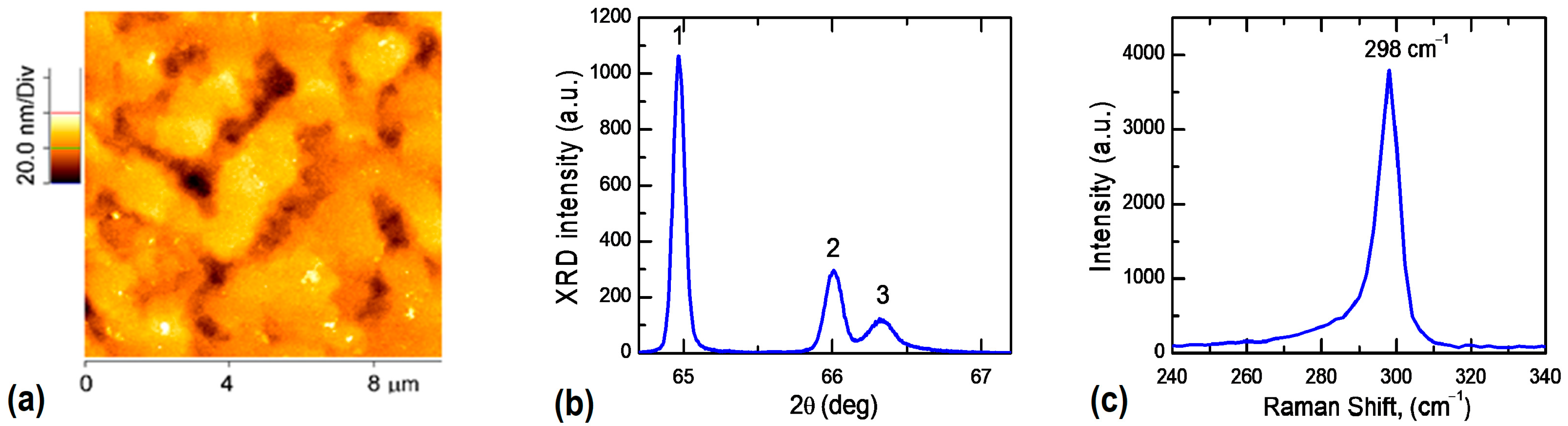
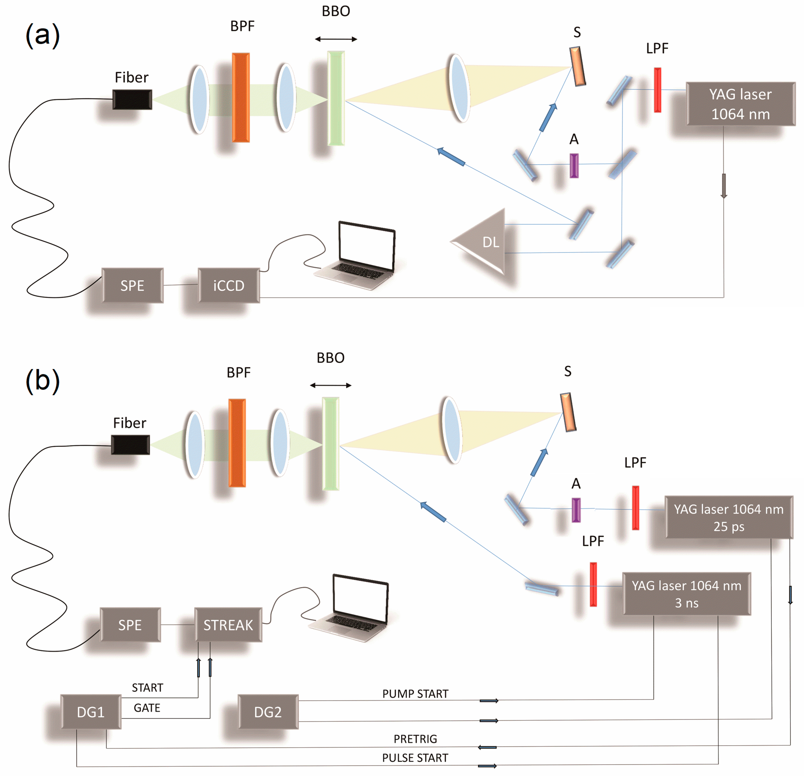
2. Materials and Methods

In this work, we tested the new infrared detection method on a 200 nm thick Ge0.95Sn0.05 layer grown on Ge/n-Si substrate by solid-source molecular beam epitaxy [7]. Firstly, on an n-type Si (001) substrate (10 kΩ·cm resistivity), a 100 nm thick Si layer was grown at 700 °C, then a 100 nm Ge layer at 350 °C was deposited by electron beam evaporation. Further, a 110 nm Ge layer was deposited at 500 °C. During this process, the bottom layers were annealed, leading to Si and Ge inter-diffusion. The final 200 nm Ge0.95Sn0.05 layer was grown at a low temperature of 150 °C and at a base pressure of 5 × 10⁻¹⁰ Torr using effusion cells equipped with dual heating filaments placed at the bottom and top of the crucible. A low growth temperature below the melting point of Sn was used to suppress Sn surface segregation. Low surface average roughness (Ra < 5 nm) (Figure 1a) and narrow XRD peaks (Figure 1b) verified the high quality of the studied layer [24]. The Raman peak position (Figure 1c) at 298 cm−1 of the LO Ge–Ge phonon shows a ~5% of Sn concentration at the GeSn epitaxial layers surface layer [24]. The value nicely coincides with the Sn content obtained by XRD [7].
For the layer excitation, we used a picosecond Nd:YAG laser EKSPLA PL2140 (1064 nm, 30 ps pulse duration, 10 Hz repetition rate, one mJ pulse energy). The pulse energy was controlled with neutral density filters. IR-pass filters blocked the laser flash lamp light. The major energy part of the same laser beam was split to be used as an optically delayed upconverting probe in a conventional setup, as shown in in Figure 2a. The developed setup with streak camera in Figure 2b employed an additional powerful nanosecond Nd:YAG laser (1064 nm, three ns, 50 mJ pulse). The pulses of the latter laser were synchronized with the aid of two generators with the picosecond laser pulses so that both pulse maxima could appear at the same time on the crystal. One generator (Delay generator PG-874, generator 2) started the flash lamp pumping of both lasers, while the other generator (Highland technology P400 digital delay and pulse generator, <10 ps jitter, 1 ps resolution, generator 1) was triggered by the picosecond laser pre-trigger. Its delayed pulses fired the nanosecond laser and started the streak camera and its time gating (100 μs gate time, used to suppress the dark counts). The nanosecond laser can be fired with a controllable delay after the sample excitation, thus allowing the slow microsecond PL decays to be measured.
We performed type II sum frequency mixing of λPL = 1100–2400 nm fluorescence light with λG = ∼1064 nm gate pulses in a 1 mm thick β-barium borate (BBO) crystal to result in upconverted light at λU = 540–740 nm [17]. This is a second-order nonlinear effect. The BBO crystal (obtained from Eksma Optics) had a cut angle θN = 41° (ϕN = 0°). The tuning plane was horizontal to the optical table. Gate pulses, transmitted through the crystal, were reflected by a 1064 nm dielectric mirror. A bandpass filter (550–900 nm) cut the second harmonic generated in the crystal. The upconverted PL was collected by a telescope with 0.12 numeric aperture and waveguide to ANDOR iStar ICCD camera with Shamrock monochromator in a conventional setup (Figure 2a). ICCD camera was gated with a 20 ns gate width. In the newly developed setup, the upconverted light was collected by the same telescope and 0.5 m waveguide to the Hamamatsu Streak camera C10627 with Acton SP2300 monochromator (200–800 nm spectral sensitivity). The streak camera operated in a photon counting regime and provided the PL spectra dispersed temporally. The spectral dispersion of the waveguide (which was measured by using supercontinuum, generated in a sapphire plate by 250 fs, 1030 nm pulses) was compensated in the measured data. The streak camera dark counts, parasitic scattering in BBO crystal, etc. limited the setup dynamic range. Few photons per one excitation pulse were enough to obtain a 10:1 signal-to-noise ratio. The wide collection angle of the infrared photoluminescence allowed the obtaining of a broad upconverted PL spectrum with a weakly variable correction function.
The new setup for streak camera sensitivity extension to infrared opens a perspective for the development of a universal broad spectral sensitivity (200–3000 nm) streak camera system with common 2D image detection and processing system, one requiring no optical delay stages needing precise alignment of the probe pulses. The streak camera can operate in a 200–900 nm spectral range within the current setup by attaching an additional light collection lens near the sample to focus the photoluminescence directly on the spectrograph slit (waveguide should be removed during the UV-VIS operation).

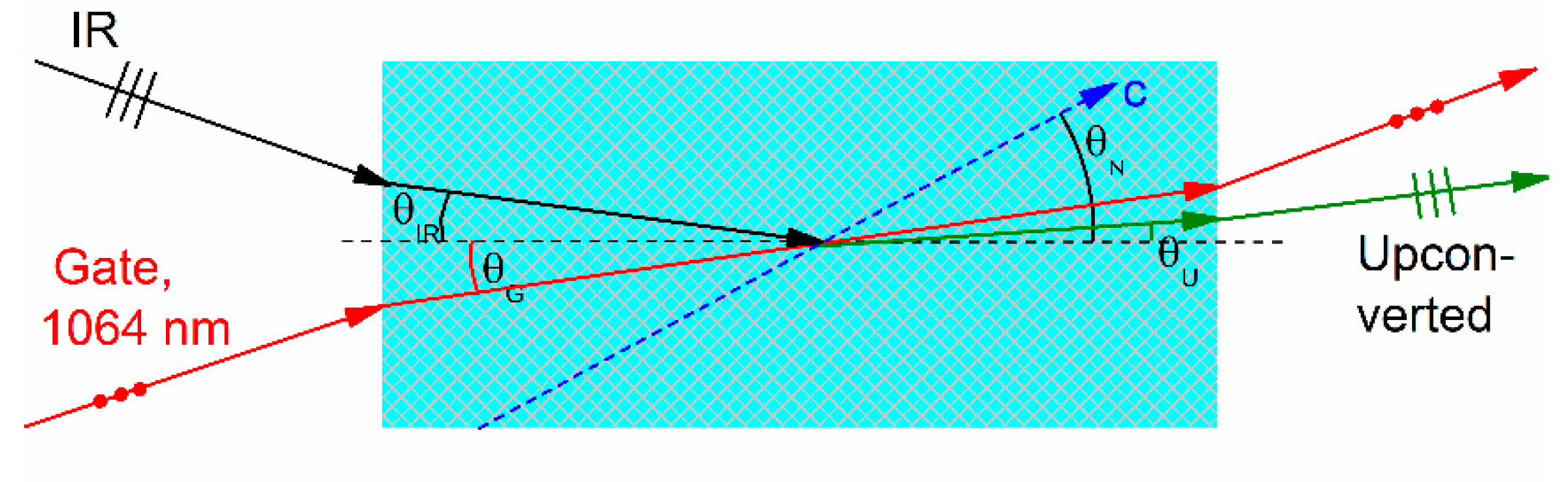
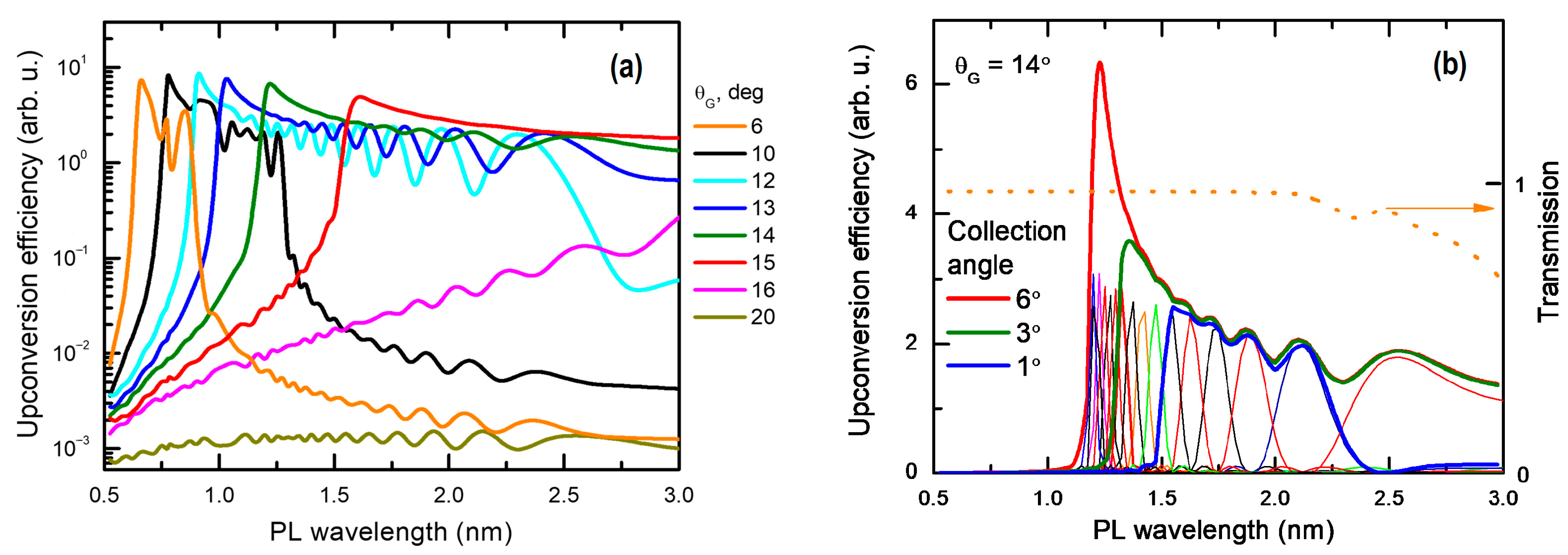
3. Theoretical Background

The scheme for phase matching in a BBO crystal is provided in Figure 3. The s polarized probe pulse was used, while the infrared and upconverted PL were p polarized. The crystal was rotated to obtain the best signal, while the probe and PL were inclined on the crystal with approximately a 15° relative angle. Further, we evaluated theoretically the broadband upconversion efficiency dependence on the phase matching angles.
For the calculations, BBO refractive index ordinary and extraordinary parts were taken from [25]. Formalism from [16] was also used. The gate refractive index ng corresponds to the ordinary refractive index n0, while the refractive indexes of the upconverted and infrared beams nu and nIR were angle-dependent. Firstly, the angle-dependent nIR according to Equation (1) was calculated,
s i n 2 ( θ I R ) n 0 2 + c o s 2 ( θ I R ) n e 2 = 1 n I R 2 ( θ I R ) .
Then, upconverted wavelength λU (1/λU = 1/λG + 1/λIR) was calculated with nu(λU) according with Equation (1). A further upconverted beam angle was calculated according to Equation (2).
n U ( θ U ) λ U s i n ( θ U ) = n I R ( θ I R ) λ I R s i n ( θ I R ) .
Infrared PL angle θIR was varied in the −6° to 6° range with a 0.5° step in calculations. Obtained θU values allowed us to calculate the wavelength-dependent upconversion intensity IUP and the phase mismatch Δkz with Equations (3) and (4) [14,16]:
I U P ( λ I R , θ I R , θ G ) = K I G I I R λ I R λ U s i n c 2 [ Δ k z ( λ I R , θ I R , θ G ) · l e f f 2 ] .
Δ k z ( λ I R , θ I R , θ G ) = 2 π [ n U ( θ U ) λ U c o s ( θ U ) n I R ( θ I R ) λ I R c o s ( θ I R ) n G λ G c o s ( θ G ) ] .
d e f f = d 22 cos 2 ( θ N + θ U ) cos ( 3 φ ) .
Here, IG and IIR are the gate and infrared photoluminescence intensities, respectively. Constant K = 32 π 5 d e f f 2 l e f f 2 ε 0 c n G n I R ( θ I R ) n U ( θ U ) s i n c 2 [ Δ k z ( λ I R , θ I R , θ G ) · l e f f 2 ] [26], deff is the effective nonlinear coefficient of BBO calculated according to [27], ε0 is the vacuum permittivity, c is the vacuum speed of light, and leff is the effective interaction length equal to the crystal thickness (1 mm). Finally, the efficiencies were summed over θIR angles to obtain wideband responses of upconversion at different θG angles (constant IR and gate intensity were assumed). The −6° to 6° infrared PL collection angle was enough to cover the entire infrared region within the 1–3 µm range. The variation of the phase matching angle for II—type phase-matching for BBO in the 1.0–2.2 μm range is only 5° (minimum is at 1.5 μm); therefore, a similar photoluminescence collection angle (±6°) allows effective broadband upconversion. The obtained upconversion efficiency curves are provided in Figure 4a. The 13–14° angle was optimal for the infrared coverage in the 1–3 µm region. The impact of the infrared PL collection angle variation for θG = 14° is shown in Figure 4b. Limiting the infrared PL angle thus allows for obtaining a narrower upconversion range. Upconversion efficiency was a few times lower for the nanosecond laser. The upconversion efficiency could be drastically improved using thicker or more efficient nonlinear crystals. Also, it should be taken into account that the picosecond laser converts only a 30 ps time interval of the decay. In contrast, the nanosecond laser converts 3 ns time interval of the decay, thus acquisition with a streak camera would be much faster if the decay is slow. (The gated upconversion needs tens to hundreds of points for the PL decay reconstruction.)

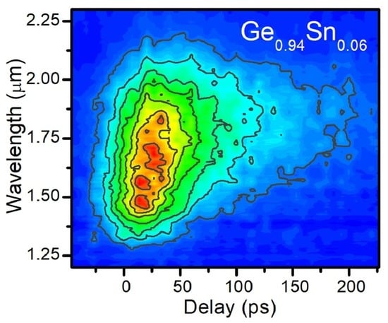
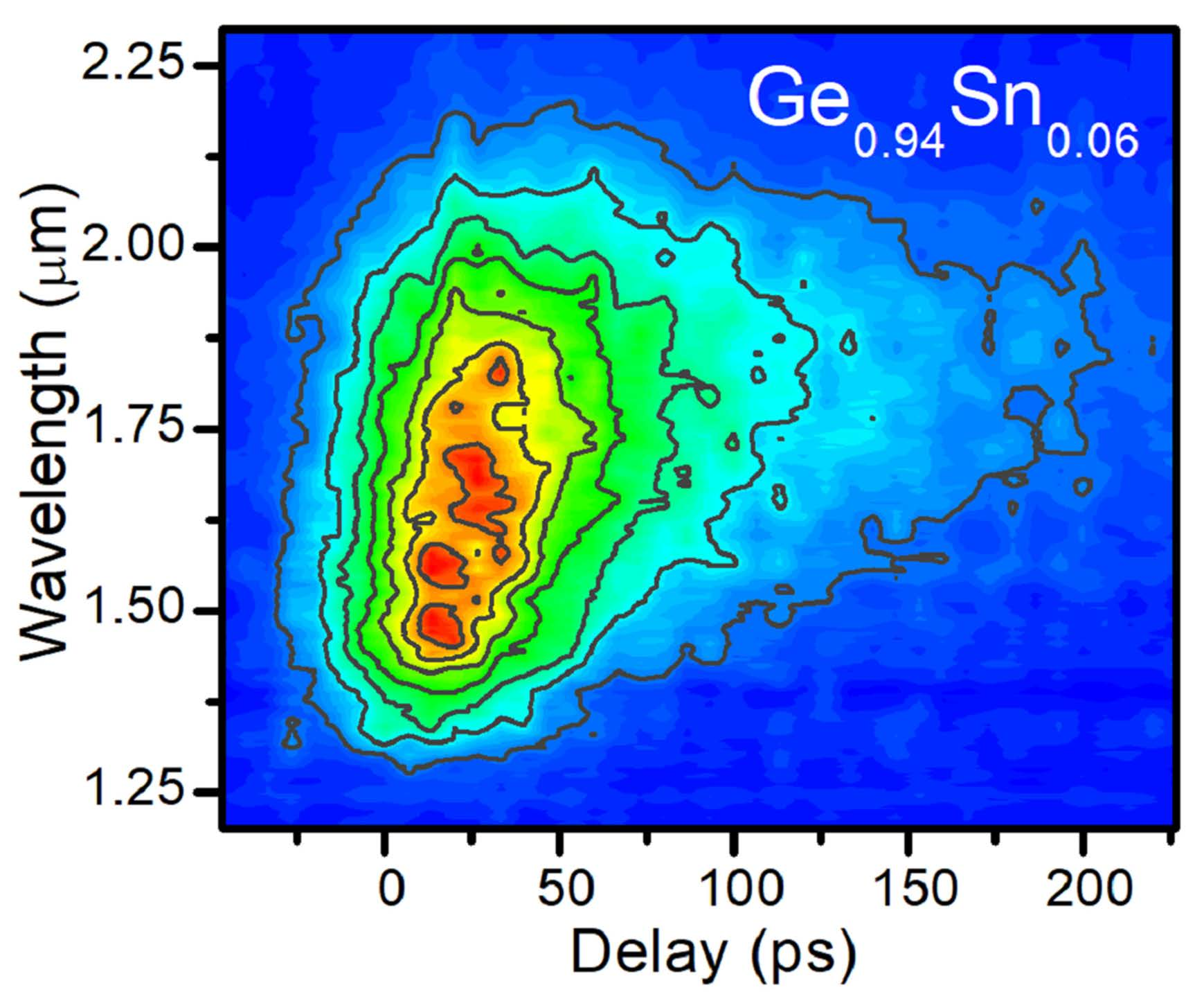
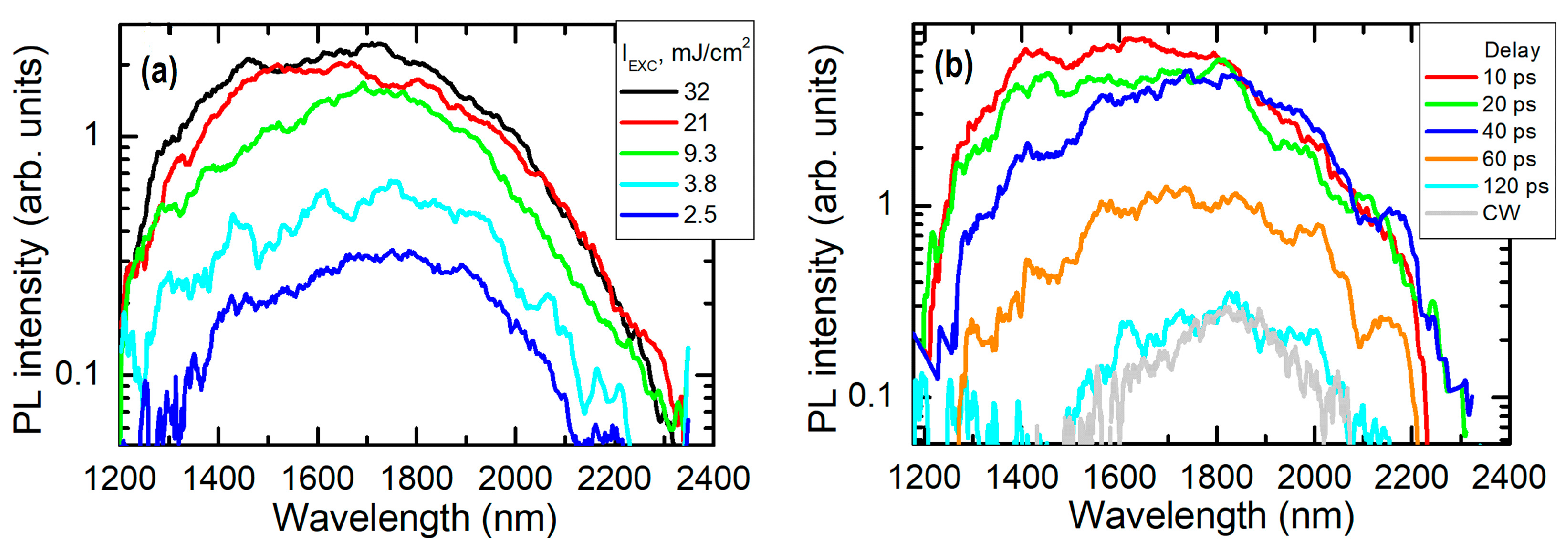
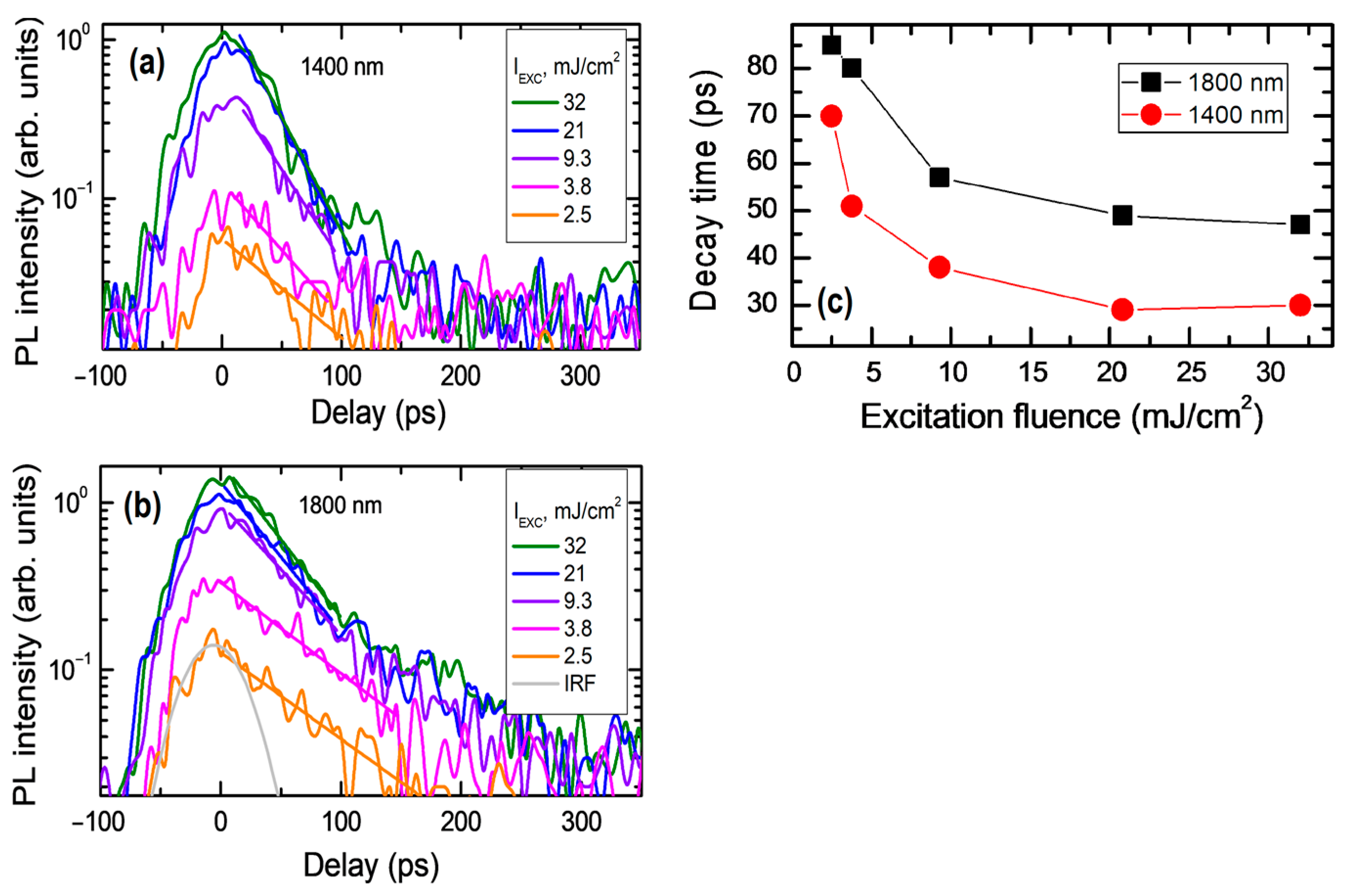
4. Results and Discussion

The experimentally measured GeSn sample PL decay map and PL decays at selected wavelengths for the conventional setup are provided in Figure 5a,b at ~30 mJ/cm2 excitation fluence. Each PL decay point corresponds to a fixed PL spectra collection time (900 shots averaged per time point was used). The spectral redshift with time is observed. Decays in the blue edge are roughly twice as fast as those in the red edge. The newly developed setup provides a comparable PL decay map (Figure 5c, collected from 18,000 shots). Figure 5d shows the temporal shape of the 1064 nm excitation pulse (scattered from a white paper sheet in the place of the sample) obtained by the upconversion with the nanosecond pulse (the upconverted signal was detected at 532 nm wavelength, slow nanosecond pulse is evident (black line) due to parasitic generation of the second harmonic in the BBO crystal). The full width at half maximum (FWHM) of the detected pulse corresponds to the setup temporal instrumental response function (IRF). An IRF function of 60 ps at FWHM was obtained; it consists of 30 ps picosecond laser pulse duration and other factors such as triggering jitter, streak camera temporal resolution (20 ps) and generator jitter (10 ps). The streak camera response function FWHMr is 56 ps for a directly detected second harmonic 532 nm pulse. (It includes generator, picosecond laser pulse duration and streak camera temporal response function.) The pulse shapes and response functions are Gaussian; thus, their summation can be approximated by normal error distribution. Therefore, the developed setup intrinsic temporal resolution FWHM (in the case when streak camera response function and excitation laser pulse durations are below ps) can be evaluated as FWHMi = (FWHMS2 − FWHMr2)1/2 = 22 ps. This intrinsic effect probably is limited by geometrical optics and nonlinearities as well as the long-term drift of triggering pulses, electromagnetic noise from nanosecond laser, etc. In Figure 5e, the spectral responsivity curve of the system is provided. The latter was measured by using the upconversion of a Xe lamp light, which was emitted from a Xe lamp (HID D2S) when it was pumped by the picosecond laser (the lamp was positioned in the same place as the sample). The measured curve corresponds to the optimal BBO crystal rotation angle (~15°) for the GeSn PL detection.
The setup with a streak camera has shown a few times lower sensitivity due to the narrow (~50 µm) streak camera slit perpendicular to the Acton SP2300 monochromator-spectrometer slit. The beam incident on the monochromator-spectrometer slit is about 400 µm in diameter; thus, a similar slit image with ~400 µm length can be observed on the imaging spectrometer output. Hence, an order of magnitude lower responsivity of the streak camera can be expected, as not all light coming from the spectrograph transfers through the streak camera slit. The latter drawback could be eliminated if the last monochromator-spectrograph (Cherny-Turner type) spherical mirror is equipped with an additional cylindrical mirror pair, transferring the outcoming large slit image from the spectrometer to a narrow line spectral image on the streak camera slit. The latter modification would also improve the streak camera’s sensitivity for visible PL measurements.
The excitation fluence- and temporally-dependent PL spectra obtained by the developed setup are provided in Figure 6. The time-integrated PL spectra in Figure 6a show gradual saturation in intensity and blue-shift with the increase of the excitation fluence. On the other hand, the time-dependent spectra in Figure 6b (at the highest excitation fluence) show redshift with time. The broadness of the PL spectra at high excitations and at the initial decay stage can be explained by filling the conduction and valence bands with carriers, leading to their degeneracy [28]. The narrower continuous waveform (CW) spectra, obtained by using an infrared ANDOR iDus spectrometer [29] at 180 mW & 805 nm excitation in the same sample, are shown for comparison in Figure 6b. They coincide well with the delayed PL spectra, which correspond to the nondegenerate carrier density.
Figure 7 shows PL decay traces and the decay times in the GeSn layer. The obtained PL decays in Figure 7 at short (integrated over 1200–1600 nm range) and long (integrated over 1600–2000 nm range) emission wavelengths have decay times similar to those in a conventional setup (see Figure 5b). The decays become faster with excitation. The calculated exponential decay times relative to the initial decay parts of the decays are shown in Figure 7c. For comparison, a similar low excitation carrier lifetime of 100 ps was obtained by a light-induced transient grating technique in the studied sample [30]. The observed reduction of the PL decay time with the excitation can be explained by the Auger recombination mechanism, which is typical for germanium [31]. PL decays at shorter emission wavelengths are faster, as they correspond to the degenerate carrier plasma, which degeneracy removes with time due to the carrier thermalization to lower energy states and their density reduction by recombination on the nonradiative defects [32].

5. Conclusions

GeSn infrared photoluminescence was effectively measured by a newly-developed cost-efficient infrared streak camera attachment based on upconversion with powerful nanosecond 1064 nm laser pulses. The setup was capable of picosecond temporal resolution limited by the streak camera jitter and excitation laser pulse duration. Spectral resolution in a 1–3 µm range was obtained with the application of a BBO crystal, covering the most investigated NIR and SWIR ranges. The excitation and time-dependent PL spectra of the GeSn layer, obtained by the new setup, agreed well with the data measured by the gated upconversion and stationary PL methods. Such measurements allowed us to obtain excitation-dependent carrier photoluminescence decay time reductions with excitation from 85 ps to 48 ps for long wavelength spectral range and from 70 ps to 30 ps for short wavelength range. Thermalization to lower energy states was observed as a redshift of PL spectra with time due to carrier density decay and their cooling with time. Moreover, the new infrared streak camera attachment opens a perspective for a universal wide spectral sensitivity (200–3000 nm) streak camera device with a common data acquisition and a processing system for the characterization of a wide scope of semiconductor films and coatings.

Author Contributions

P.Š.: project administration, methodology, investigation, data analysis, funding acquisition, writing; S.M.: methodology, investigation, data analysis; A.M.: investigation; P.O.: investigation, funding acquisition, writing and editing; H.-H.C.: writing and editing. All authors have read and agreed to the published version of the manuscript.

Funding

The research was funded by the Research Council of Lithuania under the project No. S-MIP-19-34. Pavels Onufrijevs was funded by the European Regional Development Fund within the Activity 1.1.1.2 “Post-doctoral Research Aid” of the Specific Aid Objective 1.1.1 “To increase the research and innovative capacity of scientific institutions of Latvia and the ability to attract external financing, investing in human resources and infrastructure” of the Operational Programme “Growth and Employment” (No. 1.1.1.2/VIAA/3/19/409).

Institutional Review Board Statement

Not applicable.

Informed Consent Statement

Not applicable.

Data Availability Statement

The data that support the findings of this study are available upon reasonable request from the authors.

Conflicts of Interest

The authors declare no conflict of interest.

References

  1. Göhler, B.; Lutzmann, P. Review on Short-Wavelength Infrared Laser Gated-Viewing at Fraunhofer IOSB. Opt. Eng. 2016, 56, 031203. [Google Scholar] [CrossRef] [Green Version]
  2. Yadav, P.; Dewan, S.; Mishra, R.; Das, S. Review of Recent Progress, Challenges, and Prospects of 2D Materials-Based Short Wavelength Infrared Photodetectors. J. Phys. D Appl. Phys. 2022, 55, 313001. [Google Scholar] [CrossRef]
  3. Wilson, R.H.; Nadeau, K.P.; Jaworski, F.B.; Tromberg, B.J.; Durkin, A.J. Review of Short-Wave Infrared Spectroscopy and Imaging Methods for Biological Tissue Characterization. J. Biomed. Opt. 2015, 20, 030901. [Google Scholar] [CrossRef] [PubMed]
  4. Tran, H.; Pham, T.; Margetis, J.; Zhou, Y.; Dou, W.; Grant, P.C.; Grant, J.M.; Al-Kabi, S.; Sun, G.; Soref, R.A.; et al. Si-Based GeSn Photodetectors toward Mid-Infrared Imaging Applications. ACS Photonics 2019, 6, 2807–2815. [Google Scholar] [CrossRef] [Green Version]
  5. Dong, Y.; Wang, W.; Xu, S.; Lei, D.; Gong, X.; Guo, X.; Wang, H.; Lee, S.-Y.; Loke, W.-K.; Yoon, S.-F.; et al. Two-Micron-Wavelength Germanium-Tin Photodiodes with Low Dark Current and Gigahertz Bandwidth. Opt. Express 2017, 25, 15818. [Google Scholar] [CrossRef]
  6. Cong, H.; Xue, C.; Zheng, J.; Yang, F.; Yu, K.; Liu, Z.; Zhang, X.; Cheng, B.; Wang, Q. Silicon Based GeSn P-i-n Photodetector for SWIR Detection. IEEE Photonics J. 2016, 8, 6804706. [Google Scholar] [CrossRef]
  7. Ščajev, P.; Onufrijevs, P.; Mekys, A.; Malinauskas, T.; Augulis, D.; Subačius, L.; Lee, K.; Kaupuzs, J.; Varnagiris, S.; Medvids, A.; et al. Extension of Spectral Sensitivity of GeSn IR Photodiode after Laser Annealing. Appl. Surf. Sci. 2021, 555, 149711. [Google Scholar] [CrossRef]
  8. Lee, K.; Lin, M.; Li, H.; Cheng, H.; Sun, G.; Soref, R.; Hendrickson, J.R.; Hung, K.; Scajev, P.; Medvids, A. Planar GeSn Photodiode for High-Detectivity Photodetection at 1550 Nm. Appl. Phys. Lett. 2020, 117, 012102. [Google Scholar] [CrossRef]
  9. Gnilitskyi, I.; Derrien, T.J.-Y.; Levy, Y.; Bulgakova, N.M.; Mocek, T.; Orazi, L. High-Speed Manufacturing of Highly Regular Femtosecond Laser-Induced Periodic Surface Structures: Physical Origin of Regularity. Sci. Rep. 2017, 7, 8485. [Google Scholar] [CrossRef] [Green Version]
  10. Chrétien, J.; Pauc, N.; Armand Pilon, F.; Bertrand, M.; Thai, Q.-M.; Casiez, L.; Bernier, N.; Dansas, H.; Gergaud, P.; Delamadeleine, E.; et al. GeSn Lasers Covering a Wide Wavelength Range Thanks to Uniaxial Tensile Strain. ACS Photonics 2019, 6, 2462–2469. [Google Scholar] [CrossRef]
  11. Atalla, M.R.M.; Assali, S.; Koelling, S.; Attiaoui, A.; Moutanabbir, O. High-Bandwidth Extended-SWIR GeSn Photodetectors on Silicon Achieving Ultrafast Broadband Spectroscopic Response. ACS Photonics 2022, 9, 1425–1433. [Google Scholar] [CrossRef]
  12. Zhou, Y.; Miao, Y.; Ojo, S.; Tran, H.; Abernathy, G.; Grant, J.M.; Amoah, S.; Salamo, G.; Du, W.; Liu, J.; et al. Electrically Injected GeSn Lasers on Si Operating up to 100 K. Optica 2020, 7, 924. [Google Scholar] [CrossRef]
  13. Julsgaard, B.; von den Driesch, N.; Tidemand-Lichtenberg, P.; Pedersen, C.; Ikonic, Z.; Buca, D. Carrier Lifetime of GeSn Measured by Spectrally Resolved Picosecond Photoluminescence Spectroscopy. Photonics Res. 2020, 8, 788. [Google Scholar] [CrossRef]
  14. Gerecke, M.; Bierhance, G.; Gutmann, M.; Ernsting, N.P.; Rosspeintner, A. Femtosecond Broadband Fluorescence Upconversion Spectroscopy: Spectral Coverage versus Efficiency. Rev. Sci. Instrum. 2016, 87, 053115. [Google Scholar] [CrossRef] [PubMed] [Green Version]
  15. Chosrowjan, H.; Taniguchi, S.; Tanaka, F. Ultrafast Fluorescence Upconversion Technique and Its Applications to Proteins. FEBS J. 2015, 282, 3003–3015. [Google Scholar] [CrossRef]
  16. Ashik, A.S.; O’Donnell, C.F.; Chaitanya Kumar, S.; Ebrahim-Zadeh, M.; Tidemand-Lichtenberg, P.; Pedersen, C. Mid-Infrared Upconversion Imaging Using Femtosecond Pulses. Photonics Res. 2019, 7, 783. [Google Scholar] [CrossRef]
  17. Sajadi, M.; Quick, M.; Ernsting, N.P. Femtosecond Broadband Fluorescence Spectroscopy by Down- and up-Conversion in β-Barium Borate Crystals. Appl. Phys. Lett. 2013, 103, 173514. [Google Scholar] [CrossRef]
  18. Zhang, X.-X.; Würth, C.; Zhao, L.; Resch-Genger, U.; Ernsting, N.P.; Sajadi, M. Femtosecond Broadband Fluorescence Upconversion Spectroscopy: Improved Setup and Photometric Correction. Rev. Sci. Instrum. 2011, 82, 063108. [Google Scholar] [CrossRef] [Green Version]
  19. Junaid, S.; Tomko, J.; Semtsiv, M.P.; Kischkat, J.; Masselink, W.T.; Pedersen, C.; Tidemand-Lichtenberg, P. Mid-Infrared Upconversion Based Hyperspectral Imaging. Opt. Express 2018, 26, 2203–2211. [Google Scholar] [CrossRef] [Green Version]
  20. Raissi, M.; Sajjad, M.T.; Pellegrin, Y.; Roland, T.J.; Jobic, S.; Boujtita, M.; Ruseckas, A.; Samuel, I.D.W.; Odobel, F. Size Dependence of Efficiency of PbS Quantum Dots in NiO-Based Dye Sensitised Solar Cells and Mechanistic Charge Transfer Investigation. Nanoscale 2017, 9, 15566–15575. [Google Scholar] [CrossRef]
  21. Harada, Y.; Kasamatsu, N.; Watanabe, D.; Kita, T. Nanosecond-Scale Hot-Carrier Cooling Dynamics in One-Dimensional Quantum Dot Superlattices. Phys. Rev. B 2016, 93, 115303. [Google Scholar] [CrossRef] [Green Version]
  22. ID Quantique. Available online: https://www.idquantique.com/quantum-sensing/products/id281/ (accessed on 6 January 2023).
  23. Eimerl, D.; Davis, L.; Velsko, S.; Graham, E.K.; Zalkin, A. Optical, Mechanical, and Thermal Properties of Barium Borate. J. Appl. Phys. 1987, 62, 1968–1983. [Google Scholar] [CrossRef]
  24. Perova, T.S.; Kasper, E.; Oehme, M.; Cherevkov, S.; Schulze, J. Features of Polarized Raman Spectra for Homogeneous and Non-Homogeneous Compressively Strained Ge1−ySny Alloys. J. Raman Spectrosc. 2017, 48, 993–1001. [Google Scholar] [CrossRef]
  25. Tamošauskas, G.; Beresnevičius, G.; Gadonas, D.; Dubietis, A. Transmittance and Phase Matching of BBO Crystal in the 3–5 μm Range and Its Application for the Characterization of Mid-Infrared Laser Pulses. Opt. Mater. Express 2018, 8, 1410. [Google Scholar] [CrossRef]
  26. Niu, K.; Marcus, R.A. Sum Frequency Generation, Calculation of Absolute Intensities, Comparison with Experiments, and Two-Field Relaxation-Based Derivation. Proc. Natl. Acad. Sci. USA 2020, 117, 2805–2814. [Google Scholar] [CrossRef] [Green Version]
  27. Bache, M.; Guo, H.; Zhou, B.; Zeng, X. The Anisotropic Kerr Nonlinear Refractive Index of the Beta-Barium Borate (β-BaB2O4) Nonlinear Crystal. Opt. Mater. Express 2012, 3, 357. [Google Scholar] [CrossRef] [Green Version]
  28. Scharoch, P.; Polak, M.P.; Kudrawiec, R. The Electronic Band Structure of Ge1−xSnx in the Full Composition Range: Indirect, Direct, and Inverted Gaps Regimes, Band Offsets, and the Burstein–Moss Effect. In Proceedings of the 2017 IEEE 14th International Conference on Group IV Photonics (GFP), Berlin, Germany, 23–25 August 2017; IEEE: Piscataway, NJ, USA, 2017; pp. 51–52. [Google Scholar]
  29. Ščajev, P.; Soriūtė, V.; Kreiza, G.; Nargelas, S.; Dobrovolskas, D.; Malinauskas, T.; Subačius, L.; Onufrijevs, P.; Varnagiris, S.; Cheng, H.H. Temperature and Spatial Dependence of Carrier Lifetime and Luminescence Intensity in Ge0.95Sn0.05 Layer. Mater. Sci. Eng. B Solid-State Mater. Adv. Technol. 2021, 270, 115204. [Google Scholar] [CrossRef]
  30. Ščajev, P.; Soriūtė, V.; Kreiza, G.; Malinauskas, T.; Stanionytė, S.; Onufrijevs, P.; Medvids, A.; Cheng, H.-H. Temperature Dependent Carrier Lifetime, Diffusion Coefficient, and Diffusion Length in Ge0.95Sn0.05 Epilayer. J. Appl. Phys. 2020, 128, 115103. [Google Scholar] [CrossRef]
  31. Carroll, L.; Friedli, P.; Neuenschwander, S.; Sigg, H.; Cecchi, S.; Isa, F.; Chrastina, D.; Isella, G.; Fedoryshyn, Y.; Faist, J. Direct-Gap Gain and Optical Absorption in Germanium Correlated to the Density of Photoexcited Carriers, Doping, and Strain. Phys. Rev. Lett. 2012, 109, 057402. [Google Scholar] [CrossRef]
  32. Elbaz, A.; Arefin, R.; Sakat, E.; Wang, B.; Herth, E.; Patriarche, G.; Foti, A.; Ossikovski, R.; Sauvage, S.; Checoury, X.; et al. Reduced Lasing Thresholds in GeSn Microdisk Cavities with Defect Management of the Optically Active Region. ACS Photonics 2020, 7, 2713–2722. [Google Scholar] [CrossRef]
Figure 1. (a) AFM image, XRD ω/2θ scan (b,c) micro-Raman spectra, exited by 514 nm, of Ge0.95Sn0.05 epitaxial layer. Explanation of XRD (004) peaks: (1) Ge0.95Sn0.05 fully strained on Ge; (2) Ge relaxed; (3) Si0.06Ge0.94 fully strained below Ge.
Coatings 13 00111 g001
Figure 2. Experimental time-resolved photoluminescence setups: gated upconversion (a) and streak camera upconversion (b). Here SPE—spectrometer; DG1, DG2—delay generators; DL—delay line, S—sample, LPF—low pass filter for laser flash lamp block, A—excitation energy attenuator.
Coatings 13 00111 g002
Figure 3. The upconversion experiment phase matching. Here c is the BBO crystal axis inclining at angle θN = 41° to normal of the crystal face.
Coatings 13 00111 g003
Figure 4. (a) Upconversion spectra width at 6 degree collection angle and variable θG. (b) Upconversion spectra at θG = 14° and different PL collection angles (thick lines); thin lines show upconversion spectra for fixed angles (with 0.5° step). The dotted line represents a 1 mm thick BBO crystal transmission.
Coatings 13 00111 g004
Figure 5. Upconversion with gating probe: PL map (a) and corresponding decays at different wavelengths (b). PL map upconverted with streak camera (c), temporal shape of a scattered 1064 nm excitation pulse, obtained by the upconversion with the nanosecond pumping pulse, and detected at 532 nm wavelength (d), spectral responsivity curve of the system including blocking filter (e).
Coatings 13 00111 g005
Figure 6. Excitation fluence (a) and temporal (b) dependencies of PL spectra at 32 mJ/cm2 excitation. In (b), CW spectra obtained using an infrared spectrometer are shown for comparison.
Coatings 13 00111 g006
Figure 7. Short (a) and long (b) wavelength range PL decays at different excitations, and excitation dependencies of the decay times (c). In (b), IRF corresponds to the instrumental response function. Central decay wavelengths (1400 and 1800 nm) are provided.
Coatings 13 00111 g007
Disclaimer/Publisher’s Note: The statements, opinions and data contained in all publications are solely those of the individual author(s) and contributor(s) and not of MDPI and/or the editor(s). MDPI and/or the editor(s) disclaim responsibility for any injury to people or property resulting from any ideas, methods, instructions or products referred to in the content.

