1. Introduction
As is well known, the copper indium gallium selenide (CIGS)-based solar cells have a very promising market application because of their low-cost production and long-term stability. The conversion efficiencies of CIGS solar cells in the lab have reached above 23% [
1,
2], and the commercial modules’ efficiencies have reached over 17%. CIGS has become a hot topic as an important candidate for absorber materials of high-efficiency thin film solar cells.
At present, the main modules of the absorber layer in CIGS solar cells are usually fabricated by either elemental co-evaporation of individual elements (i.e., Cu, In, Ga and Se) [
3,
4] or reactive annealing of metallic precursors (Cu-In-Ga) under an Se or H
2Se ambient environment [
5]. Co-evaporation has been widely used to prepare high-quality CIGS absorbers, because the band gap of the absorber film can easily be adjusted by this method. Commercial modules have been successfully produced by some companies (Solibro, Manz and others) using co-evaporation. Reactive annealing of metallic precursors is another popular method to prepare high-quality and large-area films. Solar Frontier has adopted this method to fabricate a solar-cell and get the efficiency of 23.35% [
1]. Although the success of these two approaches is recognized by the industrial community, a uniform absorber structure with a simple process over large areas is still challenging [
6,
7].
In recent years, some groups have researched a new way of fabricating a CIGS absorber layer by sputtering the quaternary chalcogenide target [
8,
9,
10,
11,
12]. Since the CIGS quaternary compounds in the sputtered layer processed this way have already been formed, the qualified absorber layer can be obtained without post selenization, which can greatly simplify the process of CIGS cells’ production [
9,
10] and improve the efficiency of cells in the lab to over 16% [
12]. The stoichiometry of film can be easily controlled by the sputtered target. This preparation method has the potential of industrial mass production. However, the average grain size of the CIGS absorber layer obtained in this way is smaller than that prepared by traditional processes. This is because the CIGS compounds have already been formed during sputtering from the CIGS quaternary target without annealing [
10], while the chemical activity of elements is restricted, especially of the copper, which is a key factor for grain growth [
13,
14]. To promote the grain growth of the absorber layer, in recent years, some groups have adopted the method of increasing the substrate temperature to over 600 °C [
15,
16]. This process approach is suited to the substrate with a high-melting point, such as stainless steel, but it is difficult to apply to the soda-lime glass substrates, which are widely used in the thin-film cell industry. This is the problem that must be solved to realize the industrialization of the method.
In this study, a precursor film with a Cu gradient was prepared by alternative sputtering using two quaternary targets and annealed with H2Se at 550 °C. It was proven that a better-crystallized CIGS film with a higher efficiency can be obtained by constructing a suitable bi-layer structure. This preparation method is suitable for further industrialized application, as the improved crystallization property depends on the structure of the precursor layer rather than a high annealing temperature.
2. Materials and Methods
The self-made quaternary CIGS target was used for CIGS film deposition. The CIGS bulk was synthesized in sealed quartz tubes by the particles of Cu, Ga and Se and powder of In2Se3; then, the CIGS block was broken and used as the raw material for CIGS targets sintering. Finally, the target was fabricated by hot-pressing sintering. The high density (over 99.5%) and good manufacture repeatability of target could be obtained when the Cu content in target was controlled in the range of 22.5 at. % to 25 at. %. For constructing the Cu gradient, high quality targets with a relatively bigger difference in the Cu content were a better choice. Two types of quaternary CIGS targets with 22.5 at. % and 25 at. % Cu content were used for precursor film deposition. Their compositions were (1) Cu 25 at. %, In 17.5 at. %, Ga 7.5 at. % and Se 50 at. % and (2) Cu 22.5 at. %, In 19.5 at. %, Ga 8 at. % and Se 50 at. %.
The CIGS films were deposited on the Mo-coated soda-lime glass substrate under a pressure of 0.5 Pa with a sputtering power density of 1.6 W/cm
2. Three types of precursor layers were examined. Based on previous reported studies, the thickness of the absorber film in CIGS cells with an efficiency over 15% is around 1.5 µm [
11,
12]. The different thicknesses (1.2 µm, 1.5 µm, 1.8 µm) of precursor films produced by a self-made target were also compared before this research; the 1.5-µm-thick film had better performance. Thus, the 1.5-µm-thick precursor film was chosen for investigation in this study.
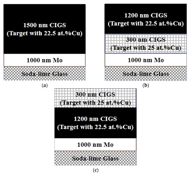
Structure 1: A 1500 nm CIGS film was deposited using a single composition target with 22.5 at. % Cu.
Structure 2: A 300-nm-thick CIGS film was deposited on the Mo surface first using a 25 at. % Cu target, and a 1200-nm-thick CIGS film was deposited sequentially using A 22.5 at. % Cu target.
Structure 3: A 1200-nm-thick CIGS film was deposited on the Mo surface first using a 22.5 at. % Cu target, and a 300-nm-thick CIGS film was deposited sequentially using a 25 at. % Cu target.
Their layer structures are shown in
Figure 1.
After deposition, the precursors were subsequently annealed in a quartz box placed in a safely sealed vacuum chamber under flowing process gas obtained by mass flow meters. The graphite heaters of the vacuum chamber could be set to a determined temperature, and the substrate temperature was detected by thermocouples in the quartz box. The experiment of the temperature-rise period was conducted under a nitrogen atmosphere of 0.5 atm. When the substrate temperature reached 300 °C, the heaters were closed, and the samples were cooled with the whole chamber. The actual substrate temperature was between 300 to 350 °C before cooling down. The selenization process was carried out in the same furnace at 550 in the H2Se (5%)/N2 atmosphere for 30 min; the treatment pressure was 0.5 atm. Then, a 50~70-nm-thick CdS layer was deposited on the CIGS absorber layer by chemical bath deposition (CBD); afterwards, an i-ZnO layer of 50 nm and AZO layer of 500 nm were deposited by magnetron sputtering under a pressure of 0.5 Pa; the sputtering power density was 0.5 W/cm2 for i-ZnO and 2.3 W/cm2 for AZO. A grid of Ni (50 nm)/Al (800 nm) was made by e-beam evaporation. Finally, the single cells were cut into square pieces with an area of 0.86 cm2 by a mechanical carving technique.
The compositions of CIGS films were analyzed by X-ray fluorescence (LAB CENTER XRF-1800). The crystalline phases were examined by X-ray diffraction (Rigaku DMAX 2500 V). The micro-morphologies were examined by a thermal field emission scanning electron microscope (TFE-SEM, Sigma, Zeiss). The variation of elements with depth were analyzed by AES (PHI-700, ULVAC-PHI). A Raman microscope (model RM2000) was used to detect the phase components. The quantum efficiency of cells was tested by a quantum efficiency tester (QE, Qtest 1000, Crown Tech). The photovoltaic (PV) performance parameters of the solar cells were measured under a current-voltage tester (Photo Emission Tech., Inc., Washington, DC, USA, CT300AAA) with a light intensity of 100 mW/cm2.
3. Results
3.1. Chemical Composition of Precursor Layers
The chemical compositions of sputtered films are shown in
Table 1. The film sputtered by a target with 25 at. % Cu was Cu-rich; the ratio of Cu/(In + Ga) reached 1.08, which does not conform to the requirement of high efficiency cells. The others were Cu-poor films, which are suitable as the absorber layer for high efficiency cells [
17].
3.2. Crystalline Properties of Annealed Layers
Figure 2 shows the SEM morphologies of annealed CIGS films. The grain size of structure 1 was small, which was about 200 nm, and the surface roughness was poor because there were many small particles on the surface (
Figure 2b). Structure 2 showed better crystallinity due to the bi-layer structure with the Cu gradient distribution (
Figure 2c) in the precursor films, on which the diffusion of the Cu element could promote the growth of grains. Its grain size could reach the micron dimension, and the surface was smooth. The annealed film with separation was observed in structure 3, in which the grain size of the upper layer was 600~800 nm, but the crystallite dimension of the bottom layer was the same as structure 1. At the same time, the presence of some small particles on the surface increased the roughness (
Figure 2f).
Figure 3 shows the XRD patterns of annealed CIGS films. From this figure, the CIGS films exhibited XRD peaks, which could be indexed to (112), (220/204) and (116/312) peaks of the chalcopyrite phases. All annealed films were crystallized with the preferable orientation of the (112) plane. The FWHM of the (112) peak in structure 2 was 0.173°, which was smaller than structure 1 (0.196°) and structure 3 (0.186°), and the intensity of the (112) peak in structure 2 was much higher than the others. This means structure 2 had the best crystalline property. This agrees well with the SEM results.
3.3. The Effect of the Cu Gradient in the Grain Growth Process
Figure 4 shows the SEM morphologies of precursor films under the temperature-rise period. The surface morphologies of structure 1 and 2 were basically the same. There were many crystalline solid phases on the surface of structure 3, which were identified as Cu–Se compounds by the Raman analysis. Structure 1 and structure 2 had similar surface characteristics in the heating period, although their compositions were different. This is because the top Cu-poor layer of structure 2 had the same composition as structure 1, and the Cu–Se phase formed in the Cu-rich layer at the bottom could hardly react with the top layer at such a low temperature.
Figure 5a shows the Raman spectra of the annealed CIGS films. It could be found that the A1 (173 cm
−1) and B2/E (215 cm
−1) peaks were present in all films [
18,
19]. This demonstrates that the CIGS phases had been formed in the annealed films. However, the peaks appeared at the position of 258–260 cm
−1 for structure 3. This indicates that the harmful Cu
2−xSe phase had been formed on the surface, which could greatly reduce the efficiency of the solar cell [
20].
Figure 5b shows the Raman spectra of the structure 3 film under different states. For structure 3, although it had a low copper content in the whole film, the Cu–Se phase could also be formed on its surface during the heating period and always existed with the annealing process. This phenomenon did not occur with structure 1 and 2, as Cu-Se phase could not be detected by the Raman at all stages compared to structure 3.
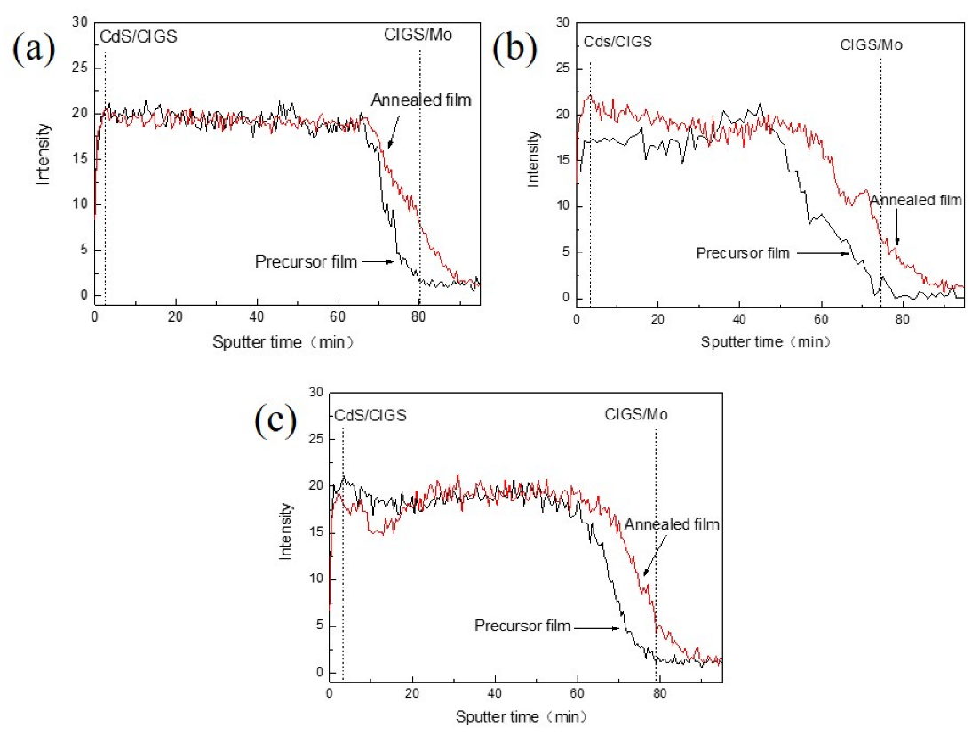
Figure 6 shows the variation of Cu elements with depth in the precursor and annealed layers. The precursor films described here had undergone the temperature-rise phase, as shown in
Figure 4. The Cu content remained consistent with the depth for the precursor film and annealed layer of structure 1. The precursor film of structure 2 exhibited back grading, with an increasing Cu content onto the back contact, and the annealed film showed front grading. This means the grain growth of structure 2 was accompanied by Cu diffusion to the front surface in the annealing process. The precursor film of structure 3 exhibited front grading, with an increasing Cu content onto the front contact, and the annealed film kept front grading.
3.4. Properties of Solar Cell
Six solar cells were made for each structure. The average performance of CIGS cells with different structures is shown in
Table 2, and the J–V curves of the devices with three different types of CIGS films are shown in
Figure 7. It was proven that all of the parameters of structure 2 with good crystallization were the best. The parameters of structure 3 with a separated annealed film were inferior compared with the others.
Figure 8 shows the external quantum efficiencies of different solar-cell devices. It indicates that the photon quantum absorbed by structure 3 was much less than that of structure 1 or 2 due to the worse quality of the absorber film with the Cu
2-xSe phase. In the 400–950-nm wavelength interval, the photon absorption of structure 1 was less than that of structure 2 because of its higher surface roughness and smaller grain size, which may have induced the loss of absorption at the interface of the CIGS and CdS layers and the CIGS absorber itself [
21]. The photon absorption of structure 1 in the range of the 950–1200-nm interval was extended towards the long wavelength for its lower index of Ga/(In + Ga).
4. Discussion
The Cu–Se liquid phase is an important factor for the crystalline property of CIGS; its occurrence and reaction determine the results of grain growth. The Cu-poor film of structure 1 had no excess Cu to form the Cu–Se phase, so the distribution of the Cu element in the film had no change before and after the annealing, and no Cu–Se phase was formed on the surface. It lacked a driving force for grain growth; the grain size of structure 1 was very small, at about 200 nm. Structures 2 and 3 had a more abundant Cu content in the precursor films than structure 1. At the grain-growth stage, Cu–Se compounds could easily be segregated at the grain surface of Cu-rich films, and the liquid phase occurred above the limit of stability of CuSe, which is at 377 °C [
22]. The annealing process under a low pressure can provide the liquid at even lower temperatures; therefore, the crystalline solid phases on the surface of structure 3 could be observed, as shown in
Figure 4, and the Cu–Se phase could be detected on the surface at a lower temperature. At the stage of a high temperature with an Se-containing atmosphere, if the amount of the Cu–Se liquid phase is more than the solid phase, the Cu–Se phase can hardly be removed, and it finally exists on the surface in the Cu
2-xSe state [
23]. When the Cu–Se liquid phase occurred on the surface of structure 3, there was no solid film in the liquid phase to react with. The Cu–Se phase tended to exist on the surface and weaken the reaction with the Cu-poor film at the bottom. As a result, the annealed film of structure 3 still maintained the Cu grading in front and had different grain sizes in the vertical direction. The grain size of the upper layer was 600~800 nm, and the grain size of the bottom layer was only 200 nm. For structure 2, there was Cu-poor upper film on the front side, and it could block the diffusion of the Cu–Se liquid phase at a low temperature. For this reason, the Cu–Se phase could not be detected on the surface of structure 2, and Cu elements presented back grading for the precursor film at the temperature-rise period. At a high temperature, the Cu-poor layer on the top could react with Cu–Se compounds; grain growth was accompanied by Cu diffusion to the front surface in this process. The distribution of Cu went from a back gradient in the temperature-rise period to a front gradient in the end. It had the uniform structure, with a big grain size over 1 µm observed by the SEM. Combined with the analysis results of the FWHM and main peak intensity given by XRD, it proved that structure 2 possessed better crystallinity. The better light absorption and conversion efficiency of cells with structure 2 are also proof from another side.
From the above results, we can reasonably conclude that the suitable Cu gradient in the precursor is a back gradient. The grain size of the absorber film based on this Cu gradient after annealing could reach the micron dimension, and a CIGS solar cell with good crystallization can have a stronger absorption of photons and the highest conversion efficiency. The unsuitable Cu gradient in the precursor is a front gradient. The Cu–Se compounds generated from the Cu-rich layer on the top could hardly be exhausted and caused a bad effect on the properties of the solar cell.
5. Conclusions
The precursor structure of Cu-poor onto Cu-rich film can take advantage of the diffusion of Cu–Se compounds in the annealing process to get a bigger grain size and smoother surface, and the formation of the Cu2-xSe phase and separated layer can be effectively prevented in this structure. The crystalline property of the CIGS film and the conversion efficiency of solar cell were improved by a precursor layer with a Cu back gradient using quaternary targets.
Author Contributions
Conceptualization, Y.L. (Yuandong Liu) and J.T.; methodology, Y.L. (Yuandong Liu) and Y.L. (Yangzheng Li); validation, Y.L. (Yuandong Liu), Y.L. (Yangzheng Li), J.T., W.Z. and B.L.; formal analysis, Y.L. (Yuandong Liu), Y.L. (Yangzheng Li) and B.L.; investigation, Y.L. (Yuandong Liu); data curation, Y.L. (Yuandong Liu) and Y.L. (Yangzheng Li); writing—original draft preparation, Y.L. (Yuandong Liu) and Y.L. (Yangzheng Li); writing—review and editing, J.T. and W.Z.; visualization, J.T.; supervision, J.T.; project administration, Y.L. (Yuandong Liu) and J.T.; funding acquisition, Y.L. (Yuandong Liu) and J.T. All authors have read and agreed to the published version of the manuscript.
Funding
This research was funded by the Project Funding of the Key R&D Program of the Science and Technology Department of Sichuan Province (Grant Nos. 2021ZYCD003 and 2021ZYD0099) and the Science and Technology Project of Southwest Petroleum University (No. 2021JBGS05).
Institutional Review Board Statement
Not applicable.
Informed Consent Statement
Not applicable.
Data Availability Statement
Data Availability Statement: Data from the study are available by request from the corresponding author.
Conflicts of Interest
The authors declare no conflict of interest.
References
- Frontier, S. Solar Frontier Achieves World Record Thin-Film Solar Cell Efficiency of 23.35%. 2019. Available online: https://www.solar-frontier.com/eng/news/2019/0117_press.html (accessed on 10 April 2019).
- Jackson, P.; Wuerz, R.; Hariskos, D.; Lotter, E.; Witte, W.; Powalla, M. Effects of heavy alkali elements in Cu(In,Ga)Se2 solar cells with efficiencies up to 22.6%. Phys. Status Solidi (RRL)–Rapid Res. Lett. 2016, 10, 583–586. [Google Scholar] [CrossRef]
- Gabor, A.M.; Tuttle, J.R.; Albin, D.S.; Contreras, M.A.; Noufi, R.; Hermann, A.M. High-efficiency CuInxGa1−xSe2solar cells made from (Inx,Ga1−x)2Se3precursor films. Appl. Phys. Lett. 1994, 65, 198–200. [Google Scholar] [CrossRef]
- Powalla, M.; Voorwinden, G.; Hariskos, D.; Jackson, P.; Kniese, R. Highly efficient CIS solar cells and modules made by the co-evaporation process. Thin Solid Film. 2009, 517, 2111–2114. [Google Scholar] [CrossRef]
- Niki, S.; Contreras, M.; Repins, I.; Powalla, M.; Kushiya, K.; Ishizuka, S.; Matsubara, K. CIGS absorbers and processes. Prog. Photovolt. Res. Appl. 2010, 18, 453–466. [Google Scholar] [CrossRef]
- Powalla, M.; Witte, W.; Jackson, P.; Paetel, S.; Lotter, E.; Wuerz, R.; Kessler, F.; Tschamber, C.; Hempel, W.; Hariskos, D.; et al. CIGS Cells and Modules with High Efficiency on Glass and Flexible Substrates. IEEE J. Photovolt. 2014, 4, 440–446. [Google Scholar] [CrossRef]
- Kushiya, K. CIS-based thin-film PV technology in solar frontier K.K. Sol. Energy Mater. Sol. Cells 2014, 122, 309–313. [Google Scholar] [CrossRef]
- Shi, J.H.; Li, Z.Q.; Zhang, D.W.; Liu, Q.Q.; Sun, Z.; Huang, S.M. Fabrication of Cu(In, Ga)Se2 thin films by sputtering from a single quaternary chalcogenide target. Prog. Photovolt. Res. Appl. 2011, 19, 160–164. [Google Scholar] [CrossRef]
- Frantz, J.A.; Bekele, R.Y.; Nguyen, V.Q.; Sanghera, J.S.; Bruce, A.; Frolov, S.V.; Cyrus, M.; Aggarwal, I.D. Cu(In,Ga)Se2 thin films and devices sputtered from a single target without additional selenization. Thin Solid Film. 2011, 519, 7763–7765. [Google Scholar] [CrossRef]
- Chen, C.-H.; Shih, W.-C.; Chien, C.-Y.; Hsu, C.-H.; Wu, Y.-H.; Lai, C.-H. A promising sputtering route for one-step fabrication of chalcopyrite phase Cu(In,Ga)Se2 absorbers without extra Se supply. Sol. Energy Mater. Sol. Cells 2012, 103, 25–29. [Google Scholar] [CrossRef]
- Rampino, S.; Armani, N.; Bissoli, F.; Bronzoni, M.; Calestani, D.; Calicchio, M.; Delmonte, N.; Gilioli, E.; Gombia, E.; Mosca, R.; et al. 15% efficient Cu(In,Ga)Se2 solar cells obtained by low-temperature pulsed electron deposition. Appl. Phys. Lett. 2012, 101, 132107. [Google Scholar] [CrossRef] [Green Version]
- Ouyang, L.; Zhuang, D.; Zhao, M.; Zhang, N.; Li, X.; Guo, L.; Sun, R.; Cao, M. Cu(In,Ga)Se2solar cell with 16.7% active-area efficiency achieved by sputtering from a quaternary target. Phys. Status Solidi 2015, 212, 1774–1778. [Google Scholar] [CrossRef]
- Zhu, X.L.; Wang, Y.M.; Zhou, Z.; Li, A.M.; Zhang, L.; Huang, F.Q. 13.6%-efficient Cu(In,Ga)Se2 solar cell with absorber fabricated by RF sputtering of (In,Ga)2Se3 and CuSe targets. Sol. Energy Mater. Sol. Cells 2013, 113, 140–143. [Google Scholar] [CrossRef]
- Xiang, Y.; Zhang, X.; Zhang, S. Insight into the mechanism of Sb promoted Cu(In,Ga)Se2 formation. J. Solid State Chem. 2013, 204, 278–282. [Google Scholar] [CrossRef]
- Bras, P.; Frisk, C.; Tempez, A.; Niemi1, E.; Platzer-Bjorkman, C. Ga-grading and Solar Cell Capacitance Simulation of an industrial Cu(In,Ga)Se-2 solar cell produced by an in-line vacuum, all-sputtering process. Thin Solid Film. 2017, 636, 367–374. [Google Scholar] [CrossRef]
- Dai, W.L.; Gao, Z.R.; Li, J.J.; Qin, S.M.; Wang, R.B.; Xu, H.Y.; Wang, X.Z.; Gao, C.; Teng, X.Y.; Zhang, Y.; et al. Above 15% Efficient Directly Sputtered CIGS Solar Cells Enabled by a Modified Back-Contact Interface. ACS Appl. Mater. Interfaces 2021, 13, 49414–49422. [Google Scholar] [CrossRef]
- Jackson, P.; Würz, R.; Rau, U.; Mattheis, J.; Kurth, M.; Schlötzer, T.; Bilger, G.; Werner, J.H. High quality baseline for high efficiency, Cu(In1−x,Gax)Se2 solar cells. Prog. Photovolt. Res. Appl. 2007, 15, 507–519. [Google Scholar] [CrossRef]
- Witte, W.; Kniese, R.; Eicke, A.; Powalla, M. Influence of the Ga content on the Mo/Cu (In, Ga) Se2 interface formation. In Proceedings of the 2006 IEEE 4th World Conference on Photovoltaic Energy Conference, Waikoloa, HI, USA, 7–12 May 2006; 1, pp. 553–556. [Google Scholar] [CrossRef]
- Delsol, T. Experimental study of graded bandgap Cu(InGa)(SeS)2 thin films grown on glass/molybdenum substrates by selenization and sulphidation. Sol. Energy Mater. Sol. Cells 2004, 82, 587–599. [Google Scholar] [CrossRef]
- Witte, W.; Kniese, R.; Powalla, M. Raman investigations of Cu(In,Ga)Se2 thin films with various copper contents. Thin Solid Film. 2008, 517, 867–869. [Google Scholar] [CrossRef]
- Hegedus, S.S.; Shafarman, W.N. Thin-film solar cells: Device measurements and analysis. Prog. Photovolt. Res. Appl. 2004, 12, 155–176. [Google Scholar] [CrossRef]
- Klenk, R.; Walter, T.; Schock, H.W.; Cahen, D.J.A.M. A model for the successful growth of polycrystalline films of CuInSe2 by multisource physical vacuum evaporation. Adv. Mater. 1993, 5, 114–119. [Google Scholar] [CrossRef]
- Park, S.-Y.; Lee, E.-W.; Lee, S.-H.; Park, S.-W.; Jung, W.-J.; Kim, W.-N.; Park, J.-S.; Seo, J.; Kim, D.-H.; Kang, J.-K.; et al. A Study on Cu(In,Ga)Se2Thin-Film Characteristics During Three-Stage Process Using Real-Time Substrate Monitoring. Mol. Cryst. Liq. Cryst. 2011, 551, 295–304. [Google Scholar] [CrossRef]
| Publisher’s Note: MDPI stays neutral with regard to jurisdictional claims in published maps and institutional affiliations. |
© 2022 by the authors. Licensee MDPI, Basel, Switzerland. This article is an open access article distributed under the terms and conditions of the Creative Commons Attribution (CC BY) license (https://creativecommons.org/licenses/by/4.0/).


