Article

Role of Materials Chemistry on Transparent Conductivity of Amorphous Nb-Doped SnO2 Thin Films Prepared by Remote Plasma Deposition

1
Institute for Energy Research, Qilu University of Technology (Shandong Academy of Sciences), 19 Keyuan Road, Jinan 250014, China
2
School of Materials Science and Engineering, Zhengzhou University, Zhengzhou 450002, China
3
International Joint Research Laboratory for Low-Carbon & Environmental Materials of Henan Province, Zhengzhou 450002, China
*
Author to whom correspondence should be addressed.
Coatings 2022, 12(8), 1111; https://doi.org/10.3390/coatings12081111
Submission received: 30 June 2022 / Revised: 1 August 2022 / Accepted: 2 August 2022 / Published: 4 August 2022
(This article belongs to the Special Issue Optical Thin Film and Photovoltaic (PV) Related Technologies)

Abstract

:
In this study, remote plasma sputtering deposition of niobium-doped SnO2 transparent conductive oxides on glass substrates was carried out at ambient temperature with no post-deposition annealing. The microstructure, optical, electrical, and surface morphology of the thin films were characterized using a combination of advanced techniques, such as X-ray diffraction (XRD), UV-Vis spectrophotometer, Hall-effect measurements, as well as field emission scanning electron microscope (FESEM), high-resolution transmission electron microscopy, and high-resolution X-ray photoelectron spectroscopy. It was determined that the oxygen defects of the films have a substantial impact on their transparent conductivity. The crystalline films, which were crystallized by annealing at 450 °C, had higher resistivities due to a decreased concentration of oxygen vacancies, which restricted conduction. In comparison, the amorphous films exhibited remarkable conductivity. The best amorphous films (Nb:SnO2) exhibited a resistivity of less than 4.6 × 10⁻³ Ω·cm, with a 3 × 1020 cm−3 carrier concentration and a 4.4 cm2/(V·S) of Hall mobility. X-ray amorphous Nb:SnO2 films can be used to make conductive and transparent protective layers that can be used to shield semiconducting photoelectrodes used in solar water splitting. These layers can also be used with more conductive TCO films (ITO or AZO) when needed.

1. Introduction

Transparent conducting oxides (TCOs) are utilized in a variety of applications, including flat panel displays, the touch screen of smartphones, tablet computers, solar cells, and light-emitting diodes [1,2]. Indium tin oxide (ITO) is the predominant TCO material due to its improved optical and electrical properties, but it has poor mechanical properties and a scarcity of resources [3]. Tin oxide (SnO2) is one of the most essential TCO materials due to its appealing characteristics, such as a wide band gap (Eg = 3.62 eV), high ultraviolet-visible (UV-vis) transmission, high electrical conductivity, high infrared (IR) reflectance, abundance in nature, lack of toxicity, and chemical stability [4,5]. Various processes, including pulsed laser deposition, chemical vapor deposition, magnetron sputtering, and chemical spray pyrolysis, have been employed to produce pure and doped-SnO2 thin solid films containing various dopants [2,6,7,8]. However, post-deposition annealing was required to increase the crystallinity of the films and acquire improved conductivity in these investigations. The films that were produced as a result exhibited poor electronic transport capabilities [9]. Recently, niobium-doped SnO2 systems were explored as an alternative material for ITO and FTO electrodes. Nb:SnO2 is expected to possess superior electronic and optical properties to ITO and FTO as TCO material. However, the Nb-doped SnO2 thin films are still not commercialized due to lack of exhaustive exploration of its electrical and optical properties by researchers [10]. To obtain a better understanding and helpful guidelines, the current paper, focused on the effects of oxygen defects on the structural, optical, and electrical properties of amorphous Nb-doped SnO2.
In this work, a systematic investigation into the deposition of X-ray amorphous, Nb-doped SnO2 films that were generated by remote plasma sputtering deposition from an alloy target is carried out. The depositions were conducted on substrates of unheated glass to investigate the potential of Nb:SnO2 films deposition on substrates sensitive to temperature (plastics) or underlying sensitive films or devices (photoelectrodes or solar cells with a thin film for water splitting). The impact of the flow rate of oxygen on the electrical characteristics of Nb:SnO2 films were thoroughly explored. These Nb:SnO2 films were designed for use as conductive and transparent protective layers for metal oxide semiconductive photoelectrodes in solar water splitting applications due to their improved chemical stability [11,12]. It can also be used as the back contact layer (electron transport layer) in different electronic and photovoltaic devices, such as diodes that emit organic light, electrochromic devices, perovskite organic-inorganic solar cells, and organic photovoltaics, due to its low electrical resistivity and high transparency [13,14,15,16,17,18].

2. Experimental

2.1. Materials and Methods

Thin films of Nb: SnO2 (Nb: 5.0 wt. %) were deposited on substrates of unheated glass (SAIL BRAND 25.4 mm × 76.2 mm and 1 mm thick) in an Ar/O2 atmosphere at room temperature by remote plasma sputtering deposition (HITUS) process at various oxygen pressures. Prior to deposition, all glass substrates were sequentially cleaned for 15 min at 50 °C with acetone, isopropyl alcohol, and deionized water in an ultrasonic bath to remove the organic contamination on the surface of the glass. The rates of gas flow for sputtering gas Ar and reactive gas O2 of 99.999% purity were 70 sccm and 0 to 5.0 sccm, respectively. The chamber pressure was adjusted to 4.0 × 10⁻³ mbar after tuning on the plasma source (PLS). The PLS power and the sputtering power applied were 500 W and 100 W, respectively. The distance between the target and substrate was kept at 35 cm. No external substrate heating occurred during the deposition procedure.

2.2. Material Characterization

Thin-film structural characterization was examined using X-ray diffraction (XRD) on a Rigaku Corporation (Ultima IV) operated in theta-2theta geometry with a monochromatized Cu Kα radiation over the scan range from 20° to 80°. At room temperature, an ultraviolet-visible spectrophotometer (UV-3600) was utilized to measure the optical transmittance from 300 to 800 nm. The electrical transport characteristics of the film, such as Hall mobility, carrier density, and resistivity, were investigated at room temperature using a Hall measuring device (Hall 8400) and the van der Pauw method. The cross-sectional microstructure, thickness, particle size, and surface morphology of a film were assessed using a field emission scanning electron microscope (FESEM Sirion-200). The electron binding energy and surface composition of Sn 3d, Nb 3d, and O 1s orbit were examined utilizing an X-ray photoelectron spectrometer (XPS, Thermo K-Alpha) with Al-Kα X-ray (1486.6 eV) at 100 W and 15 kV, and C 1s was selected at 284.8 eV as a standard for calibration when interpreting the data. To examine the morphology, as well as the grain size, scanning electron microscopy (SEM) was carried out using a FESEM that was equipped with energy-dispersive spectroscopy (EDS). Photoluminescence spectra that were temperature-dependent were obtained by using a fluorescence spectrophotometer (Edinburgh FLS-920) with a xenon lamp (300 W) as the excitation source. We employed nearly the same excitation power for measuring the PL spectra of samples stimulated at different wavelengths by varying the incidence slit width. This implies that the PL intensities obtained were comparable. To calibrate the sensitivity factor for oxygen, a pristine sample of SnO2 (Aladdin) was used as a reference. The short-range structure and vibration modes were analyzed by Raman spectroscopy (HORIBA Scientific LabRAM HR Evolution) with a laser excitation wavelength of 325 nm (spot size: ∼1 um in diameter).

3. Results and Discussion

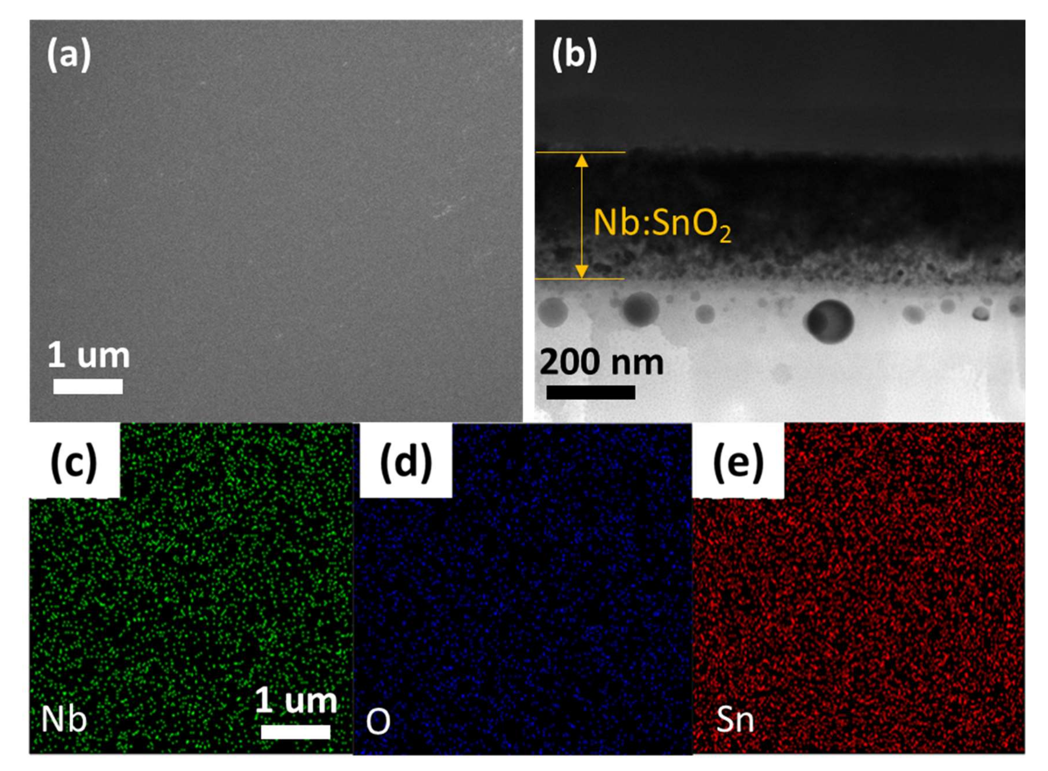
3.1. Characterization of Structure and Morphology

Figure 1a illustrates the XRD patterns of the as-deposited films at varying oxygen flow rates. The absence of diffraction peaks supports the amorphous nature of these X-ray films. The Raman spectra (not shown) of as-deposited Nb:SnO2 films exhibited only weak, wide characteristics that correspond to the glass substrates. Raman spectroscopy is capable of detecting structural characteristics and phases for crystallite sizes in the few nm range, which is lower than what is attainable using XRD; therefore, it was determined that the films of Nb:SnO2 are truly amorphous [19]. Figure 1b shows the XRD patterns of the produced thin films of Nb:SnO2 after being post-annealed at 450 °C for 15 min. It is clearly indicated that amorphous films transform into rutile tin dioxide (PDF#41-1445) [20]. The thin-film diffraction peaks revealed sharp (110) and minor (101), (200), (211), and (301) orientations [21]. Moreover, the partial pressure of oxygen during deposition affected the crystallinity. No peaks for the SnO, Sn2O3, or Sn phases were detected, showing that the thin films were completely oxidized. The XRD patterns revealed no Nb oxide phases, indicating that Nb replaced Sn in the tetragonal lattice.
Figure 2a presents the morphology for the Nb:SnO2 sample deposited at room temperature. The surface of the sample exhibits relatively smooth and dense. Based on the cross-sectional SEM image presented in Figure 2b, it was determined that the film had an average thickness of around ∼240 nm. EDS mapping was also carried out on a selected film area, as illustrated in Figure 2c–e. These spectra clearly confirm the existence of Sn, Nb, and O elements on the surface of Nb doped SnO2 thin films. The Nb, Sn, and O EDS signals appear to be uniformly dispersed across the entire film. The average Nb/(Nb + Sn) ratio is about (0.05 ± 0.01) measured from different area of several films, which corresponds to about 5 at% of Nb incorporation into SnO2 in Nb:SnO2 thin films.

3.2. Optical and Electrical Properties

In the visible region (300–900 nm), Figure 3a depicts the transmittance spectra of the as-deposited films with varying oxygen flow rates. The films became increasingly transparent in the visible spectral range as the flow rate of oxygen increased. Optical transmittance increased from 75% to 92% when oxygen flow was increased, which might be explained by an increase in crystallite size and a decrease in grain boundary scattering. The edge of absorption moves to shorter wavelengths. The film optical band gap was determined by plotting (inset of Figure 3a) (ahv)2 against hv, where a denotes the absorption coefficient and hv denotes the photon energy. The optical band gap increased slightly with increasing oxygen flow rate, from 3.80 to 4.02 eV. This enhancement in the energy of the optical band gap is attributable to the Burstein–Moss effect [20].
Figure 3b depicts the Hall mobility, concentration of carrier, and electrical resistivity of as-deposited Nb:SnO2 films as a function of O2 flow rate. It demonstrates that the O2 flow rate had a significant impact on the film’s resistivity and carrier concentrations. The quantity of oxygen vacancies correlates with the Nb:SnO2 film carrier concentrations deposited under a partial pressure of oxygen. The vacancy of one oxygen produced two more electrons in the film; hence, oxygen vacancies were the primary source of free electrons. The concentration of carriers increases as the number of oxygen vacancies increases. Deficiencies (oxygen vacancies) developed first and subsequently decreased as the oxygen flow rate increased. In general, a semiconductor’s electrical conductivity is driven by the Hall mobility and concentration of carriers, as shown below: ρ = 1/eμn, where ρ denotes the resistivity, n denotes the number of charge carriers, e is the carrier’s charge, and μ is the mobility. An oxygen flow rate at which a minimum resistivity is achieved results in a local maximum in the concentration of carriers and a maximum Hall mobility. As a result, the resistivity reduces as the flow rate of oxygen increases from 3.0 to 4.0 sccm, achieves a minimum at 4.0 sccm (4.3 × 10⁻³ Ω·cm), and subsequently increases for oxygen flow rates greater than 4.0 sccm.

3.3. XPS Analysis

XPS measurements were performed on amorphous and annealed Nb:SnO2 thin films to assess the electrical structure and oxidation state of Nb and Sn, respectively. The high-resolution spectra of as-deposited and annealed thin films of Nb 3d are shown in Figure 4a,b. Both spectra revealed two extremely symmetric peaks caused by spin-orbit splitting, revealing a single oxidation state designated as Nb5+. The binding energies of 206.53 and 206.92 eV can be assigned for the d 5/2 lines, which is 1 eV greater than that of the tetravalent state (205.7 eV). This finding is consistent with the previously reported data, demonstrating that the majority of Nb is already in its most oxidized state at the time of deposition. As a result, we estimate that the lower valence Nb species were oxidized during thermal treatment. No metallic bonds, such as Sn–Nb, were present in the films. It has been shown that much of Nb can ionize into Nb5+ and substitute Sn4+ so that one free electron can be contributed from each Nb atom [22]. According to DFT calculations, it is difficult for the substitutional state of Nb Sn to form under an O-rich situation (annealed films) because its formation energy is substantially higher than that for a native defect such as the Sn vacancy (VSn) [23].
Figure 4c shows the fitting peaks of the Sn 3d spectrum from the as-deposited Nb:SnO2 thin films. As evidenced by the fluctuating proportion of the two detected components, the peak deconvolution process revealed a crucial feature of the surface chemistry of the samples. The surface of the Nb:SnO2 film showed mostly Sn4+ (B.E. of 486.29 eV for 3d 5/2 and 494.75 eV for 3d 3/2) and a small amount of Sn2+ (B.E. of 485.38 eV for 3d 5/2 and 493.90 eV for 3d 3/2). There was no evidence of elemental Sn0 atom contribution at B.E. around 485 eV [24]. Since there was less oxygen in the sputtering process, the entire sputtering system would be in an oxygen-deficient environment, resulting in incomplete oxidation of the Sn. This is also the primary reason why tin occurs in a low-valence state. The binding energies of the fitted peaks were in good agreement with other reports in the literature. Figure 4d shows a highly symmetric Sn 3d peak for annealed Nb:SnO2 thin films, indicating one single oxidation state which is identified as Sn4+ from the binding energy of 494.77 eV and 486.3 eV [25]. The low formation energy of the acceptor-like Sn vacancy (VSn) can assist in scavenging electrons from their ionization, hence decreasing the film conductivity in annealed films (O-rich condition). On the other hand, the high formation energy of VSn prevents the spontaneous development of native electron killers and, thus, increases the film conductivity in the as-deposited films (O-poor condition).
Figure 4e displays the fitting peaks of the O 1s spectrum from the as-deposited Nb:SnO2 thin films. Since a simple visual study of the shape of the XPS O 1s peak revealed that it is wide and asymmetrical in this instance, it is apparent that it must comprise many components. The XPS O 1s peak decomposition of Nb:SnO2 thin films indicated that they are composed of three components. Specifically, the major O 1s peak appeared at 529.7 eV and was attributed to oxygen in the lattice [26]. The minor peak with the highest energy, 531.9 eV, belongs to hydroxyl species adsorbed to the surface [27]. The oxygen-deficient portions of the matrix of Nb:SnO2 were found to have a medium binding energy component, which was observed at 531 eV. This component was connected with O2−. The intensity of this peak may be linked to changes in the concentration of oxygen vacancies (VO) [28]. Native donor-like defects, such as VO, have lower formation energy, which can aid to prevent the spontaneous generation of native electron killers and, hence, lower the film resistivity. Figure 4f shows the fitting peaks of the O 1s spectrum from the annealed Nb:SnO2 thin films. The fit of the O 1s peak showed that the surface contains mostly lattice oxygen species (530.1 eV) and there is a higher proportion of surface adsorbed hydroxyl species (531.9 eV). No evidence was observed from the oxygen vacancy contribution, indicating that high-temperature annealing decreased the oxygen vacancies in the samples (sufficient oxidation) [29].
Overall, the low formation energy defects of NbSn, VO, and high formation energy of VSn aid in preventing the production of native electron killers in the as-deposited films. In contrast, it is difficult to form NbSn and VO due to the higher formation energy than VSn in the annealed films. VSn tends to act as an acceptor-like defect and will deteriorate the conductivity of the film. At the same time, NbSn and VO should also be eliminated due to the formation of deep donor transition levels.

3.4. Fluorescence Spectroscopy

It is generally known that the optical characteristics of oxide semiconductors are influenced by both intrinsic and extrinsic factors. To confirm the nature of defects, PL spectra were performed on as-deposited Nb:SnO2 thin films at varying oxygen flow rates. Figure 5a depicts the emission spectra at room temperature of films formed at varying oxygen flow rates. The broadly visible luminescence exhibited in Nb:SnO2 thin films is mostly due to self-trapped excitons and oxygen vacancy defect states. When the oxygen flow rate reached 4.0 sccm, the peak’s intensity increased significantly, indicating a significant increase in the concentration of native defects. When the flow rate was increased to 5.0 sccm, the peak’s intensity decreased. The drop in luminescence PL intensity at 715 nm was caused by a decrease in oxygen vacancy concentration. Recombination of in-diffused oxygen with oxygen vacancies reduces the concentration of oxygen vacancies [30,31]. The deconvolution of the peak was essential to acquiring a clear understanding of the factors that led to the broad PL emission (Figure 5b). The broad emission peak might be effectively described by two Gaussian bands centered at 748 nm and 695 nm, respectively. The peak at 748 nm may be ascribed to oxygen vacancy-associated trap states and self-trapped excitons, whereas the peak at 695 nm is probably associated with an intrinsic defect contribution [32].

4. Conclusions

Amorphous Nb:SnO2 films were deposited on glass substrates at low temperatures by remote plasma sputtering deposition. The electrical, mechanical, and optical properties of the as-deposited films were measured as a function of the O2 flow rate. The best amorphous Nb:SnO2 films had a resistivity of better than 4.6 × 10⁻³ Ω·cm with a carrier concentration of 3 × 1020 cm−3, and Hall mobility of 4.4 cm2/(V·S). This is due to the low formation energy of NbSn and VO and the high formation energy of VSn help to avoid the formation of these native electron killers. Due to its superior chemical stability, such Nb:SnO2 films are intended for applications as transparent and conductive protection layers for metal oxide semiconducting photoelectrodes for solar water splitting.

Author Contributions

The manuscript was written through contributions of all authors. Conceptualization and methodology, A.S.; formal analysis and investigation, Y.W., S.L. and Q.W.; writing and original draft preparation, A.S.; writing, review and editing, A.S. and J.H. All authors have read and agreed to the published version of the manuscript.

Funding

This research was funded by the National Key Research and Development Program of China (2021YFB4001802-03) and Excellent Young Scholars of the Natural Science Foundation of Shandong Province (2022HWYQ-090) and Scientific and Education Program of Qilu University of Technology (Shandong Academy of Sciences) (No. 2022PX047 and 2022GH010).

Institutional Review Board Statement

Not applicable.

Informed Consent Statement

Not applicable.

Data Availability Statement

Data is contained within the article.

Conflicts of Interest

The authors declare no conflict of interest.

References

  1. Anaraki, E.H.; Kermanpur, A.; Mayer, M.T.; Steier, L.; Ahmed, T.; Turren-Cruz, S.-H.; Seo, J.; Luo, J.; Zakeeruddin, S.M.; Tress, W.R. Low-temperature Nb-doped SnO2 electron-selective contact yields over 20% efficiency in planar perovskite solar cells. ACS Energy Lett. 2018, 3, 773–778. [Google Scholar] [CrossRef]
  2. Ramarajan, R.; Kovendhan, M.; Thangaraju, K.; Joseph, D.P. Indium-free large area Nb-doped SnO2 thin film as an alternative transparent conducting electrode. Ceram. Int. 2020, 46, 12224–12231. [Google Scholar] [CrossRef]
  3. Dong, L.; Zhu, G.; Xu, H.; Jiang, X.; Zhang, X.; Zhao, Y.; Yan, D.; Yuan, L.; Yu, A. Preparation of indium tin oxide (ITO) thin film with (400) preferred orientation by sol–gel spin coating method. J. Mater. Sci. Mater. Electron. 2019, 30, 8047–8054. [Google Scholar] [CrossRef]
  4. Thomas, B.; Skariah, B. Spray deposited Mg-doped SnO2 thin film LPG sensor: XPS and EDX analysis in relation to deposition temperature and doping. J. Alloys Compd. 2015, 625, 231–240. [Google Scholar] [CrossRef]
  5. Guo, R.; Zhao, Y.; Zhang, Y.; Deng, Q.; Shen, Y.; Zhang, W.; Shao, G. Significant performance enhancement of all-inorganic CsPbBr3 perovskite solar cells enabled by Nb-doped SnO2 as effective electron transport layer. Energy Environ. Mater. 2021, 4, 671–680. [Google Scholar] [CrossRef]
  6. Song, J.; Xu, X.; Wu, J.; Lan, Z. Low-temperature solution-processing high quality Nb-doped SnO2 nanocrystals-based electron transport layers for efficient planar perovskite solar cells. Funct. Mater. Lett. 2019, 12, 1850091. [Google Scholar] [CrossRef] [Green Version]
  7. Hirano, T.; Tsuboi, T.; Tanabe, E.; Ogi, T. In-situ flame deposition of Pt catalysts on Nb-doped SnO2 nanoparticles. J. Alloys Compd. 2022, 898, 162749. [Google Scholar] [CrossRef]
  8. Fu, Q.; Halck, N.B.; Hansen, H.A.; Lastra, J.M.G.; Vegge, T. Computational study of Nb-doped-SnO2/Pt interfaces: Dopant segregation, electronic transport, and catalytic properties. Chem. Mater. 2017, 29, 1641–1649. [Google Scholar] [CrossRef]
  9. Zhang, G.; Qin, G.; Yu, G.; Hu, Q.; Fu, H.; Shao, C. Ab initio investigation on a promising transparent conductive oxide, Nb:SnO2. Thin Solid Films 2012, 520, 5965–5970. [Google Scholar] [CrossRef]
  10. Seo, Y.J.; Kim, G.W.; Sung, C.H.; Anwar, M.S.; Lee, C.G.; Koo, B.H. Characterization of transparent and conductive electrodes of Nb-doped SnO2 thin film by pulsed laser deposition. Curr. Appl. Phys. 2011, 11, S310–S313. [Google Scholar] [CrossRef]
  11. Song, A.; Levine, I.; van de Krol, R.; Dittrich, T.; Berglund, S.P. Revealing the relationship between photoelectrochemical performance and interface hole trapping in CuBi2O4 heterojunction photoelectrodes. Chem. Sci. 2020, 11, 11195–11204. [Google Scholar] [CrossRef] [PubMed]
  12. Luo, J.; Steier, L.; Son, M.-K.; Schreier, M.; Mayer, M.T.; Grätzel, M. Cu2O nanowire photocathodes for efficient and durable solar water splitting. Nano Lett. 2016, 16, 1848–1857. [Google Scholar] [CrossRef] [PubMed]
  13. Kakinuma, K.; Chino, Y.; Senoo, Y.; Uchida, M.; Kamino, T.; Uchida, H.; Deki, S.; Watanabe, M. Characterization of Pt catalysts on Nb-doped and Sb-doped SnO2–δ support materials with aggregated structure by rotating disk electrode and fuel cell measurements. Electrochim. Acta 2013, 110, 316–324. [Google Scholar] [CrossRef]
  14. Senoo, Y.; Kakinuma, K.; Uchida, M.; Uchida, H.; Deki, S.; Watanabe, M. Improvements in electrical and electrochemical properties of Nb-doped SnO2−δ supports for fuel cell cathodes due to aggregation and Pt loading. RSC Adv. 2014, 4, 32180–32188. [Google Scholar] [CrossRef]
  15. Savych, I.; Subianto, S.; Nabil, Y.; Cavaliere, S.; Jones, D.; Rozière, J. Negligible degradation upon in situ voltage cycling of a PEMFC using an electrospun niobium-doped tin oxide supported Pt cathode. Phys. Chem. Chem. Phys. 2015, 17, 16970–16976. [Google Scholar] [CrossRef] [PubMed] [Green Version]
  16. Stefik, M.; Cornuz, M.; Mathews, N.; Hisatomi, T.; Mhaisalkar, S.; Grätzel, M. Transparent, Conducting Nb:SnO2 for Host–Guest Photoelectrochemistry. Nano Lett. 2012, 12, 5431–5435. [Google Scholar] [CrossRef] [PubMed]
  17. Song, A.; Plate, P.; Chemseddine, A.; Wang, F.; Abdi, F.F.; Wollgarten, M.; van de Krol, R.; Berglund, S.P. Cu:NiO as a hole-selective back contact to improve the photoelectrochemical performance of CuBi2O4 thin film photocathodes. J. Mater. Chem. A 2019, 7, 9183–9194. [Google Scholar] [CrossRef] [Green Version]
  18. Liang, Y.; Tsubota, T.; Mooij, L.P.A.; van de Krol, R. Highly Improved Quantum Efficiencies for Thin Film BiVO4 Photoanodes. J. Phys. Chem. C 2011, 115, 17594–17598. [Google Scholar] [CrossRef]
  19. Mientus, R.; Weise, M.; Seeger, S.; Heller, R.; Ellmer, K. Electrical and Optical Properties of Amorphous SnO2:Ta Films, Prepared by DC and RF Magnetron Sputtering: A Systematic Study of the Influence of the Type of the Reactive Gas. Coatings 2020, 10, 204. [Google Scholar] [CrossRef] [Green Version]
  20. Díaz, E.C.Y.; Camacho, J.M.; Duarte-Moller, A.; Castro-Rodríguez, R.; Bartolo-Pérez, P. Influence of the oxygen pressure on the physical properties of the pulsed-laser deposited Te doped SnO2 thin films. J. Alloys Compd. 2010, 508, 342–347. [Google Scholar] [CrossRef]
  21. Wang, W.; Feng, X.; Luan, C.; Ma, J. Effect of Nb doping on structural and electrical properties of homoepitaxial rutile TiO2:Nb films. Ceram. Int. 2018, 44, 2432–2435. [Google Scholar] [CrossRef]
  22. Kamisaka, H.; Hitosugi, T.; Suenaga, T.; Hasegawa, T.; Yamashita, K. Density functional theory based first-principle calculation of Nb-doped anatase TiO2 and its interactions with oxygen vacancies and interstitial oxygen. J. Chem. Phys. 2009, 131, 034702. [Google Scholar] [CrossRef] [PubMed]
  23. Han, X.; Song, K.; Lu, L.; Deng, Q.; Xia, X.; Shao, G. Limitation and extrapolation correction of the GGA + U formalism: A case study of Nb-doped anatase TiO2. J. Mater. Chem. C 2013, 1, 3736–3746. [Google Scholar] [CrossRef]
  24. Rizzato, A.P.; Santilli, C.V.; Pulcinelli, S.H.; Messaddeq, Y.; Hammer, P. XPS Study of the Corrosion Protection of Fluorozirconate Glasses Dip-Coated with SnO2 Transparent Thin Films. J. Sol-Gel Sci. Technol. 2004, 32, 155–160. [Google Scholar] [CrossRef]
  25. Szuber, J.; Czempik, G.; Larciprete, R.; Koziej, D.; Adamowicz, B. XPS study of the L-CVD deposited SnO2 thin films exposed to oxygen and hydrogen. Thin Solid Films 2001, 391, 198–203. [Google Scholar] [CrossRef]
  26. Song, A.; Chemseddine, A.; Ahmet, I.Y.; Bogdanoff, P.; Friedrich, D.; Abdi, F.F.; Berglund, S.P.; van de Krol, R. Evaluation of Copper Vanadate (β-Cu2V2O7) as a Photoanode Material for Photoelectrochemical Water Oxidation. Chem. Mater. 2020, 32, 2408–2419. [Google Scholar] [CrossRef]
  27. Song, A.; Berglund, S.P.; Chemseddine, A.; Friedrich, D.; Abdi, F.F.; van de Krol, R. Elucidating the optical, electronic, and photoelectrochemical properties of p-type copper vanadate (p-Cu5V2O10) photocathodes. J. Mater. Chem. A 2020, 8, 12538–12547. [Google Scholar] [CrossRef]
  28. Wei, S.; Wang, C.; Long, X.; Wang, T.; Wang, P.; Zhang, M.; Li, S.; Ma, J.; Jin, J.; Wu, L. A oxygen vacancy-modulated homojunction structural CuBi2O4 photocathodes for efficient solar water reduction. Nanoscale 2020, 12, 15193–15200. [Google Scholar] [CrossRef] [PubMed]
  29. Fondell, M.; Gorgoi, M.; Boman, M.; Lindblad, A. An HAXPES study of Sn, SnS, SnO and SnO2. J. Electron Spectrosc. Relat. Phenom. 2014, 195, 195–199. [Google Scholar] [CrossRef] [Green Version]
  30. Santara, B.; Giri, P.K.; Imakita, K.; Fujii, M. Evidence of oxygen vacancy induced room temperature ferromagnetism in solvothermally synthesized undoped TiO2 nanoribbons. Nanoscale 2013, 5, 5476–5488. [Google Scholar] [CrossRef] [PubMed]
  31. Sinha, S.K.; Bhattacharya, R.; Ray, S.K.; Manna, I. Influence of deposition temperature on structure and morphology of nanostructured SnO2 films synthesized by pulsed laser deposition. Mater. Lett. 2011, 65, 146–149. [Google Scholar] [CrossRef]
  32. Yu, S.; Li, L.; Sun, Z.; Zheng, H.; Dong, H.; Xu, D.; Zhang, W. Characteristics of Transparent Conducting W-Doped SnO2 Thin Films Prepared by Using the Magnetron Sputtering Method. J. Am. Ceram. Soc. 2015, 98, 1121–1127. [Google Scholar] [CrossRef]
Figure 1. The XRD patterns of the as-deposited thin films (a) and after annealing at 450 °C (b) under different oxygen flow rates.
Coatings 12 01111 g001
Figure 2. FESEM (a) surface image and (b) cross-section image of the as-deposited Nb-doped SnO2 thin film. The elemental mapping of (c) Nb, (d) O, and (e) Sn. Nb:SnO2 thin films deposited at 4.0 sccm of oxygen flow rate.
Coatings 12 01111 g002
Figure 3. (a) Optical transmittance of Nb:SnO2 thin films are plotted as a function of wavelength deposited at varying flow rates of oxygen, with an inset showing the fluctuation of band gap (Eg) at various oxygen flow rates. (b) The electrical characteristics of Nb:SnO2 films are plotted as a function of various flow rates of oxygen deposited at room temperature.
Coatings 12 01111 g003
Figure 4. Deconvoluted XPS spectra of Nb 3d, Sn 3d, and O 1s of the as-deposited (a,c,e) and the annealed (b,d,f) Nb:SnO2 thin films deposited at 4.0 sccm of oxygen flow rate.
Coatings 12 01111 g004
Figure 5. (a) The PL spectra of the Nb:SnO2 thin films as a function of O2 flow rate. (b) PL spectra of the thin films after fitting at the O2 flow rate of 4.0 sccm. All the spectra are excited by the 300 nm line of a xenon lamp.
Coatings 12 01111 g005
Publisher’s Note: MDPI stays neutral with regard to jurisdictional claims in published maps and institutional affiliations.

