Article

Growth Mechanisms of TaN Thin Films Produced by DC Magnetron Sputtering on 304 Steel Substrates and Their Influence on the Corrosion Resistance

by
Milton David Serna-Manrique
1,
Daniel Escobar-Rincón
1,2,*,
Santiago Ospina-Arroyave
1,
Daniel Alejandro Pineda-Hernández
1,
Yury Paola García-Gallego
1 and
Elisabeth Restrepo-Parra
1
1
Laboratorio de Física del Plasma, Universidad Nacional de Colombia–Campus La Nubia, Manizales 170003, Colombia
2
Departamento de Física y Matemática, Universidad Autónoma de Manizales, Manizales 170002, Colombia
*
Author to whom correspondence should be addressed.
Coatings 2022, 12(7), 979; https://doi.org/10.3390/coatings12070979
Submission received: 14 June 2022 / Revised: 4 July 2022 / Accepted: 6 July 2022 / Published: 11 July 2022

Abstract

:
In this work, thin films of TaN were synthesized on 304 steel substrates using the reactive DC sputtering technique from a tantalum target in a nitrogen/argon atmosphere. All synthesis parameters such as gas ratio, pressure, gas flow, and substrate distance, among others, were fixed except the applied power of the source for different deposited coatings. The effect of the target power on the formation of the resulting phases and the microstructural and morphological characteristics was studied using XRD and AFM techniques, respectively, in order to understand the growth mechanisms. Phase, line profile, texture, and residual stress analysis were carried out from the X-ray diffraction patterns obtained. Atomic force microscopy analysis allowed us to obtain values for surface grain size and roughness which were related to growth mechanisms in accordance with XRD results. Results obtained showed a strong correlation between the growth energy with the crystallinity of the samples and the formation of the possible phases since the increase in the growth power caused the samples to evolve from an amorphous structure to a cubic monocrystalline structure. For all produced samples, the δ-TaN phase was observed despite the low N2 content used in the process (since for low N2 content it was expected to be possible to obtain films with α-Ta or hexagonal ε-TaN crystalline structure). In order to determine the corrosion resistance of the coatings, electrochemical impedance spectroscopy and polarization resistance were employed in the Tafel region. The results obtained through this evaluation showed a direct relationship between the power used and the improvement of the properties against corrosion for specific grain size values.

1. Introduction

Transition metal nitrides have been a type of material of great interest, being widely studied for their importance both in fundamental science and in a wide range of technological applications [1,2]. Between their highlighted characteristics, mechanical properties, such as high hardness and thermal stability, as well as the high melting point, classify transition metal nitrides as refractory materials. Resistance to wear and friction and resistance to corrosion make them very important compounds in applications for protective coatings of structures, which are generally made of steel, cutting tools, and reconstruction of worn parts. Likewise, these compounds have excellent electrical and thermal conductivity, high chemical stability, low diffusion, and adequate adherence [3,4,5,6,7]. For all these properties that have made nitride materials of vital importance, great efforts have been devoted to the study of transition metal nitrides to find hard and resistant materials that meet the growing demand that has been generated in recent decades in various applications, as already mentioned [8,9]. For these purposes, tantalum nitride (TaN), as a hard coating, was initially not as attractive as titanium nitride (TiN), zirconium nitride (ZrN), and their alloys, probably due to their high cost and the difficulty of achieving successful synthesis [10]. Furthermore, depending on the amount of nitrogen (N2) incorporated, TaN shows a great variety of crystalline phases such as cubic, hexagonal, tetragonal, and orthorhombic, which cause multiple and sensitive changes in its properties [11,12]. However, tantalum nitride has recently attracted great interest as a protective coating due to its excellent properties such as good wear and corrosion resistance, super hardness, high strength and toughness (even at high temperatures), high thermal stability, and great thermal conductivity [4,11,12,13]. These properties position this material as a great candidate for different applications such as diffusion barriers, an application in which it has achieved a great reputation [14,15], silicon-based integrated circuits, high-performance microprocessors and in a wide variety of biomedical applications, showing that these coatings have better histocompatibility and hemocompatibility than traditionally used biomedical alloys [16,17]. Additionally, the superconductor TaN has been shown to be a much better candidate than niobium nitride (NbN) for the detection of single photons [15] due to its smaller space and lower density of states. This material also works well as a normal state barrier as Josephson crosses [18]. Previous work has found that TaN coatings significantly improve the corrosion resistance of stainless steels (austenitic), which is mainly due to their character as an inert material. They even, for tests of Bode diagrams, showed that the resistance to polarization is maintained over time [19].
In order to fully understand the structural properties of TaN coatings and thus be able to design these materials for a specific application, it is necessary to study the physical and chemical mechanisms involved during the film growth process. It is well known that, in the case of the magnetron sputtering technique, models have been identified, the best known being those that represent the mechanisms of (i) Van der Merwe, which corresponds to growth by monolayers, (ii) Volmer–Weber mechanism, that corresponds to the three-dimensional growth of nuclei, and (iii) Stranski–Krastanov (S-K) mechanism, in which the formation of a deformed or pseudomorphic structure occurs followed by nucleation of clusters in such altered layer [18,20]. These mechanisms are generally described in terms of thermodynamic or surface energy aspects. Aspects include the absorption, desorption and diffusion of atoms, deformations in the crystal lattice of the surface, reconstruction of the surface, or relaxation of the crystal lattice of the surface. These phenomena cause the spacing between atoms or the crystallographic structure of the surface to change, producing amorphous crystalline mixtures [21]. On the other hand, although it has been reported that the three variables that most affect the growth of the coating are temperature, pressure, and argon to nitrogen ratio [22,23,24], there are other variables present in the process that can influence the energies of the particles and their mobility both in the plasma and on the substrate, as the growth power [25]. Considering that there are few reports where the structure, microstructure, and morphology of TaN are related to applied power in the DC magnetron sputtering technique alongside a corrosion analysis, the novelty of this work is framed in the contribution to the knowledge of how this material grows in an important technique as important parameters like power, is varied.
This work evaluated the influence of applied power in a reactive DC magnetron sputtering technique on the microstructure and morphology of TaN coatings. The main goal was to identify growth mechanisms based on material parameters like crystalline structure, microstructure, and surface parameters like morphology and their relation to power. Subsequently, the behavior of the corrosion resistance of these materials was evaluated using potentiodynamic techniques. The study of the microstructure and the present phases and morphology was carried out using X-ray diffraction techniques (XRD) and atomic force microscopy (AFM), respectively. On the other hand, the corrosion resistance was evaluated by means of electrochemical impedance spectroscopy.

2. Materials and Methods

The TaN films were grown in a TORUS® 2 inches Kurt–Lesker magnetron sputtering system (Kurt J. Lesker, Clairton, PA, USA) on AISI-SAE 304 steel substrates. The substrate surface was prepared by mechanical polishing to generate a mirror-like finish in order to decrease the rugosity which allows for the evaluation of the roughness of the coating generated during growth. Subsequently, the substrates were taken to a bath in an ultrasonic cube to free them of particulate and organic materials. Then, the chamber was evacuated at a base pressure of 1.1 × 10⁻³ Pa. When this pressure was reached, the entry of gases was carried out. Initially, argon was introduced, in order to perform a target cleaning process (plasma cleaning) eliminating the impurities present on the target surface. The deposition of the coatings was carried out at a constant pressure of 666 × 10−3 Pa, in a mixture of Ar and N2, with constant fluxes of 22.5 and 2.5 sccm, respectively. A tantalum target, with a purity of 99.99%, was placed on the cathode and the substrates were placed in an electrically floating piece, at a distance of approximately 19.2 cm to the plasma source. The synthesis of the coatings was carried out by varying the applied power with values of 120, 150, 160, 170, 180, 190, 200, 210, and 220 W. The diffraction measurements were carried out with a Bruker D8 Advance diffractometer with a beam wavelength of λ = 1.5406 Å, corresponding to the kα1 line of a copper X-ray tube, and with a scintillation point detector. Measurements were made in asymmetric diffraction in a grazing incidence method, where the incident angle was fixed to 4 degrees meanwhile the detector scanned from 30 to 75°. The angular step was set at 0.02° and the time per step was 5 s. The equipment was calibrated with the Lanthanum Hexaboride (LaB6) 660 °C sample from the National Institute of Standards and Technology (NIST). Lattice parameters were calculated from peak positions associated with the peak with the best statistics (intensity to noise ratio) and higher angle, where the error in the interplanar distance, calculated from Bragg’s law, are lower. Crystallite size and microstrain values were calculated using the Williamson–Hall method [26] and texture coefficients were obtained from Harris method [27].
For the morphological characterization of the samples, surface measurements were made with a scanning probe microscope (SPM) (AFM 5100, HITACHI, Tokyo, Japan) in dynamic force microscopy (DFM) or non-contact mode, using a silicon (Si) tip type N whose radius of curvature is 6 nm, frequency of 300 KHz and a spring constant (C) of 80 N/m. 5 and 1 μm2 scans were made, with a resolution of 512 pixels × 512 lines, and frequencies recommended by the equipment software. Finally, for the evaluation of the corrosion resistance, a Gamry 1000 E potentiostat/galvanostat (Warminster, PA, USA) was used using the EIS techniques and resistance to polarization in the Tafel region. A corrosive medium, 0.5 M H2SO4 was used. The mentioned equipment is located in the Plasma Physics Laboratory of the National University of Colombia, in Manizales City, Colombia.

3. Results and Discussion

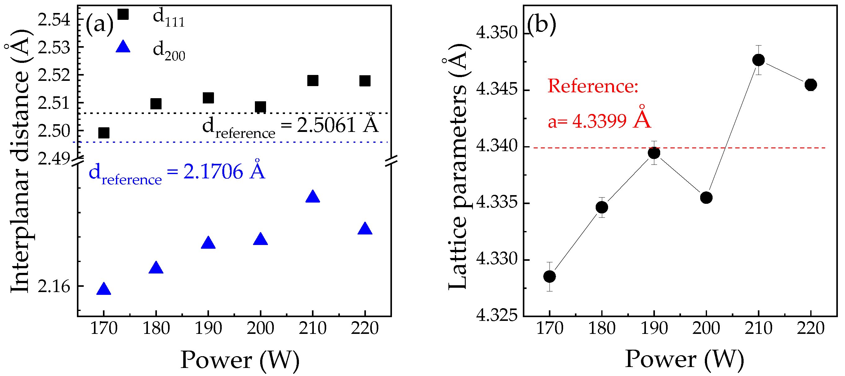
3.1. X-ray Diffraction Analysis

Figure 1 shows the diffraction patterns of the films prepared at different powers applied to the tantalum target and the simulated diffraction pattern (at the bottom of the figure in the black line) corresponding to the identified phase based on the database. In all measurements, only the reflections associated with the atomic planes (111), (200), (220), and (311) of the δ-TaN phase (JCPDS 49-1283 crystallographic card [28]) were identified, for 2θ values at 35.7°, 41.6°, 60.3°, and 72.2°, respectively.
The interdiffusion effects and the influence of the substrate surface on the formation and evolution of the phase in the different planes are negligible because, when the films are deposited at room temperature, the substrates only act as flat surfaces for deposition [29]. H. B. Nie et al. [29] and S. Xu et al. [30] coincide in their findings, reporting that, as the nitrogen content increases in the growth process, an evolution occurs that goes from an α-Ta phase to a δ-TaN phase passing through a hexagonal ε-TaN phase, showing that the structure δ-TaN is a stable structure in a wide range of nitrogen concentration. It should be noted in this work that, given the low nitrogen content, the increase in growth power led to the unique formation of the cubic structure δ-TaN. However, V. F. Petrunin et al. [31] report the successful manufacture of δ-TaN by self-propagating high-temperature synthesis (SHS) at a temperature of 1200 °C; likewise, Sung-II Baik and Young Woon Kim [32], through TEM measurements, observed that, as the growth power increases, the formation and good definition of a columnar structure corresponding to the δ-TaN phase is favored, and furthermore, that it becomes a dominant phase for growth at high powers, even for different nitrogen concentrations. It is clear then, that there is a minimum kinetic energy for the formation of this structure, that is to say, that it is a structure characterized by high formation energies, even for nitrides of other elements such as boron, titanium [33], molybdenum, tungsten, rhenium, hafnium, and zirconium [34]. Therefore, high powers improve the mobility of the ions, both Ta and N2, stabilizing the structure in a high-temperature regime, where high diffusion and absorption are favored, as well as low desorption of the atoms of nitrogen reaching the substrate.
The interplane distances dhkl for the most representative intensities are shown in Figure 2a. A comparison with the values taken from the crystallographic database [28] allows the observation of, in most cases, a tensile stress for d111 and a compressive stress for d200.
However, the mean value of the lattice parameter, calculated by taking all the indexed peaks in each pattern (see Figure 2b), shows a compressive stress at 170 and 180 W, tensile at 210 and 220 W, and a general increase in its magnitude for the highest power values. Indeed, it has been reported that the growth power produces a more significant variation of the residual stress in the films for the tensile stress intervals, than for those of compressive stress [35]. Since the coatings were made at a low partial pressure of nitrogen, the energetic ions have a considerable mean free path and a high momentum with low collision frequency, which then causes a compressive stress initially in the films, where a fibrous and dense structure can be expected, as reported by Takuya Yoshihara and Katsumi Suzuki [36]. As the growth power increases, the number of collisions also increases, and it goes to a tensile regime with a microstructural evolution with grains of small columns with low-density grain limits at the film/substrate interface, as reported by L.A Clevenger et al. [37].
For microstructural analysis, the Williamson–Hall method was used with an instrumental resolution function calculated from a lanthanum hexaboride (LaB6) standard sample through the Caglioti equation [38]. Figure 3 shows the results obtained for both the crystallite size (black squares and black arrow) and the microstrain (red circles and red arrow). It is possible to observe a wide range of values for the size of the crystalline domain, which varies between 60 and 125 nm.
As the power increases, there is a slight decrease in the crystallite size parameter to the minimum value (55.46 nm) corresponding to the 200 W sample. For higher power values, the crystallite size increases to the maximum values (~124 nm). We can identify three behaviors mainly for the parameter in question, which are the increase for the range 170–180 W and 200–210 W, a decrease for the range 190–200 W, and invariance for powers of 180–190 W and 210–220 W.
The power applied to the target is generally directly associated with the energy with which the species reaches the substrate, since argon atoms, highly energetic, provide translational kinetic energy to the adatoms [39,40,41]. For this reason, as the power increases in sputtering deposition processes, it is expected that diffusion processes are promoted and, therefore, the growth of crystallite size and crystallinity [42]. This behavior corresponds, then, to two regions of Figure 3, where the increase in power leads to this change. The growth of the crystallite related to the lower powers (170, 180, and 190 W) is accompanied by a decrease in microstrain, which, although slight, is associated with the disappearance of domain boundaries given the favoring of the crystallization of the material.
The decrease in crystalline domain size, that is observed between the powers of 190 and 200 W does not constitute normal behavior at the levels of microstrain shown in Figure 3. This implies that there is an additional mechanism to diffusion, which generates a refinement in the crystallite with low microstrain. H. N. Shah et al. [43] have stated that the increase in power is associated with the increase in the flux density of the species, and therefore with the increase in the collision frequency. The latter would result in a greater loss of energy in the adatoms and, therefore, in a reduction in the crystallization processes on which the crystallite size depends, without compromising variations in microstrain, considering that the change in this last parameter is not very representative, with respect to powers less than 200 W. Finally, for higher power values, an increase in both microstrain and crystallite size is evidenced. For this last parameter, such an increase may be associated with the fact that the applied power reaches levels where a flow of high density and energy of the species is generated, which would “reactivate” the diffusion mechanism and therefore the domain sizes have reached a higher crystalline size. For the increase of microstrain, another characteristic mechanism of sputtering processes, with the high energy of species, must be coupled to the one previously described. This process corresponds to the bombardment of reactive and neutral species against the growing coating. This process generates a collisional displacement of atoms in their ideal atomic positions, creating local defects in the material [44,45].
On the other hand, Figure 4 shows the results of the calculation of the texture coefficient by means of the Harris method [27]. The dotted lines represent the values of the texture coefficients for a powder sample (from the database), which does not have a contribution due to preferential orientation developed in the crystallization process and therefore will act as a reference. In contrast to the results obtained from the microstructure, from the aforementioned results, the three regions characterized by “low”, “medium”, and “high” powers are not evident. In this case, for the power of 170 W, an almost texture-free sample is produced, where the difference from powder preferential orientation is negligible.
An increase in power generates a considerable change in orientation with respect to all directions ((111), (200), and (220)) since there is a strong preferential orientation towards the peak of (111) resulting in the representative decrease of (200), and (220) plane orientations. For the 190 W power, the texture coefficients closely match those of the theoretical standard, with a slight favor to the (111) direction as a result of a decrease of the (220) peak. The increase in power to a value of 200 W generates an abrupt change in the preferential orientation totally opposite to the 180 W sample, since, for this sample, the preferential orientation is given for growths directed along the (200) orientation, sacrificing growth in the (111) and (220) directions. For the higher value powers, in the case of the one synthesized at 210 W, there is a similarity with respect to the 200 W sample, but not as representative, since there is a decrease in orientation along (200) and an increase for both (111) and (220). Finally, the 220 W sample exhibits a slight preferential growth along the (111) and (200) directions.
As has been reported in other research, the evolution of texture is related to crystallization processes, which are characterized by the deposition energy. Low deposition energies lead to preferential orientation related to recrystallization of the grains that have the lowest nucleation energy [45]. It is observed then, from Figure 4, that there is a competition in the preferential orientation of crystallographic planes (111) and (200), that varies following a defined behavior. As source power increases, preferential orientations change gradually from (111) to (200) at constant texture values for the (220) peak. For the sample grown with 200 W, (200) texture reaches its maximum and at the highest power values (210 W and 220 W), (111) texture increases with the decrement of (200) texture, until the values become approximately equal, slightly above to that corresponding to the free texture TaN sample, meanwhile, (220) texture remains below this reference. This clearly shows that there is a direct relation between ion energies reaching the substrate (related to power source) and preferred orientation of growth, which is shown in texture variations, and where those energies reach a certain value, energies of adatoms favored both (111) and (200) orientation of growth, due to the tendency towards a structural conformation of lower surface energy [46,47]. Mentioned competition, in our case, is due to the energy of the incident ions and to a lesser extent to the flow ratio of gas ions to metal (which may vary due to cathode poisoning), which cause strong anisotropy in potential energies and diffusion of surface mobile species [48], where possibly, there is a competition between surface energy and surface elastic surface energy.
In this way, the results lead to determine that the growth mechanisms that are imposed in the formation of thin films of cubic tantalum nitride in its δ phase are constituted by good diffusion linked to the high growth energies, which lead to the high mobility of target-dwelling species. This promotes homogeneous nucleation that leads to a good crystallization of the phase, where the reflections for the smaller angles associated with the planes (111) and (200) generally prevail, as the growing power increases and this becomes evident with increasing crystallite size. There is no evidence in our results of a possible re-evaporation of the deposited material or effects of possible polluting agents.

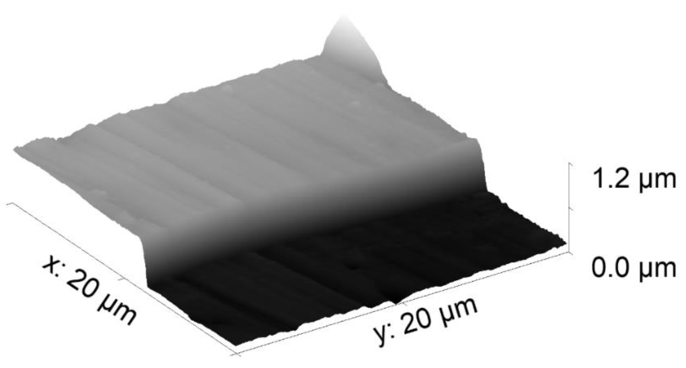
3.2. Scanning Probe Microscopy Analysis

Analysis of thickness, roughness, and grain size was performed using the AFM technique in DFM in a non-contact mode [35]. Figure 5 shows a representative image used to measure the thickness of the coatings corresponding to the sample grown at 210 W. The thickness values for all the samples are shown in Table 1, where an increase in the deposition rate is evidenced, this correlated with the increase in the applied power in the deposition process [49].
Morphological analysis of TaN coatings was based on surface roughness Rq (Rms) and the grain size. An example of AFM micrographs, showing surface morphology at different scales, is shown in Figure 6, for a sample grown at 210 W.
In general, all measurements resulted in low roughness without representative abrupt grain height variations. This can be evidenced in the values reported in Table 2, where considering the error, roughness does not exceed 30 nm approximately. It is important to note that grooves associated to the polishing procedure on the AISI 304 steel, were also observed in some regions of the surface coating, hence, morphological statistical analysis was made focusing the measurement region where these grooves are not present.
An increase in the roughness of the films at 120, 190, and 220 W can be observed in Figure 7, where grain definition is evident as deposition source power increases. It has been shown that amorphous surface morphology, referring to those surfaces with shallower depressions or channels and hence a smoother finish, are produced at low deposition source power. As power increases, the formation of deeper channels and the protrusion of grain start to occur, increasing roughness. The last step of the mentioned mechanism is related to crystallization processes favored by power increments (see Figure 1), where a defined crystal flat surface should start to show decreasing roughness [50,51,52]. It is evident that the range of power applied in this work does not reach the values that favor the mentioned surface flatting process. In the case of the present work, applied power only enables the definition of the grain increasing roughness.
The transition from amorphous surface morphology to a defined grain surface structure can be explained by the tendency of grain size, as power in the deposition process, is augmented. This behavior is shown in Figure 8. For samples deposited at 150 W, a high grain size varying from 70 to 120 nm is observed, which can be related to irregularity or an amorphous surface topography. In this sense, large size cumulates of coating result in a high size grain and the same occurs for small size cumulates, resulting in low size grains.
This is the reason for the high error observed for this data point. As applied power is increasing, these amorphous large grains start to shrink (samples grown at 160, 170, and 190 W) as a consequence of the definitions of crystalline grains on the surface and subsequently, at higher power values, grains grow as a consequence of recrystallization processes [50]. From the results shown in Figure 2 and Figure 8, it is evident that for some samples, crystallite size becomes higher than grain size, which can be assumed as an unusual result. Nevertheless, it is important to note that crystallite size, given by line profile analysis, is measured along the direction of growth of the coating, and the grain obtained from the AFM technique is a lateral measurement (along the plane of the coating); therefore, for non-homogeneous materials, like coatings and thin films, where the biaxial length are considerably larger than the thickness of the material, crystallite and grain size are not always measured along the same direction.

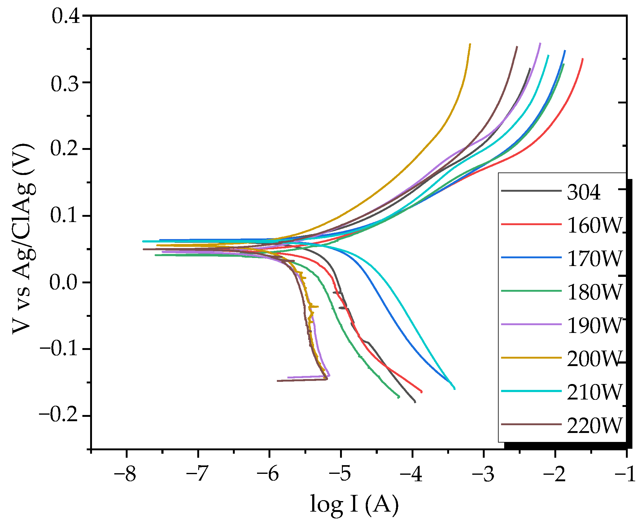
3.3. Corrosion Resistance Analysis

The potentiodynamic polarization curves in the Tafel region for the different coatings, grown at different powers, are shown in Figure 9. It can be observed how the samples grown at 180, 190, 200, and 220 W move at anodic potentials with respect to austenitic 304 steel, which represents a more noble tendency of the surface [53].
Samples 160 W, 170 W, and 210 W, show cathodic potentials, which implies more aggressive corrosion, as can be corroborated in Table 3. This corrosion mechanism is further supported by the corrosion rates presented. Table 3 also shows the calculated values of corrosion current (Icorr), corrosion potential (Ecorr), polarization resistance (Rp), and corrosion rate. The results show an increase in the polarization resistance through the increase in the synthesis power, exhibiting values of the order of kΩ cm2, giving the coatings a good protective efficiency. The high resistance to polarization can be attributed to a thin passive inert layer of Ta2O5 that forms in this type of nitride [54]. In previous investigations, it has been constantly reported that physical vapor deposited (PVD) coatings are characterized by possessing different types of defects such as holes, cracks, and impurities, among others, due to their chemical composition, structure, and deposition parameters. In aggressive environments, these defects can be direct paths to the substrate, thus causing localized corrosion and a decrease in protective efficiency [55].
The energy with which the material strikes the growing film during its deposition can also influence the density of these defects through the variation of the energy with which the ions reach the surface of the substrate, which could influence the atomic distribution surface and generate changes in the corrosive behavior of the coatings. The protective efficiencies of the coatings are listed in Table 3.
Additionally, comparing the corrosion rate and the grain size at different growth powers, it was observed that there is an inverse correlation; the higher the grain, the lower the corrosion resistance of the coatings, mainly attributed to the decrease in the number of grain boundaries [56]. In Table 3, it is presented how corrosion resistance behaves with increasing growth power.

3.4. Electrochemical Impedance Spectroscopy (EIS)

The behavior of impedance as a function of frequency is shown in Figure 10a. The Bode diagram corresponding to the phase angle in Figure 10b clearly shows two-time constants for samples 160 W and 210 W. The peak at high frequencies is related to the capacitive behavior of the coating and the peak at low frequencies to the capacitive behavior of the substrate in pores [57].
The loss of phase shift for some samples at low frequencies represents the loss of the dielectric properties of the substrate in the pores, which makes the accumulation of charge between the two interfaces (coating-electrolyte and substrate-electrolyte) hardly distinguishable. The attempt to form a significant phase shift at low frequencies shown by samples 170, 180, 190, 200, and 220 W may represent a sudden loss of the passive oxide layer formed in the pores, indicating that the electrolyte reached the substrate much more invasively than in the other samples. The diffusion of some reactants such as oxygen through the system depends largely on the type of grain boundaries present in the pores of the coating. For this reason, the microstructure of the coatings is related to the diffusive behavior [58], which could give us indications of a possible columnar structure in samples 170, 180, 190, 200, and 220 W, and an equiaxed or amorphous vitreous structure in samples 160 and 210 W that showed a significant lag. Furthermore, the austenitic 304-steel substrate showed highly capacitive behavior only at high frequencies, which gives an indication of its low porosity [59].

4. Conclusions

  • The successful synthesis of tantalum nitride has been achieved using the reactive DC sputtering technique and the effect of growth power on phase formation and microstructure has been investigated to reach an understanding of the growth mechanisms that predominate in the formation of the compound;
  • Despite the fact that TaN is a material that is characterized by its great richness and coexistence of phases, with the parameter configuration used in this work, nanocrystalline films of the cubic δ-TaN structure were obtained for source power above 170 W, despite the low nitrogen content used, where it was then expected to obtain α-Ta or hexagonal ε-TaN; below this value, amorphous phases were obtained;
  • Growth mechanisms were identified to be strongly related to the energy of ions reaching the substrate, where stress transition from compressive to tensile as applied power increases according to a variation in lattice parameter from 4.32 to 4.34 Å (free lattice parameter for δ-TaN is 4.34 Å), is related to energy decrement of nitrogen ions due to the collision frequency variations as a function of power;
  • Conventional diffusion increment of adatoms on the growing coating is favored as power goes from 170 W to 190 W, which is evidenced by the increment of crystallite size from 50 nm to 100 nm approximately. Subsequently, when power is increased to 200 W, an abnormal lowering in crystallite size is observed, implying an additional mechanism for diffusion, which consists of the collision frequency increment for Ta and N atoms, associated with adatom energy loss. Finally, higher power values lead to reactivation of diffusion processes due to the fact that energy loss due to collisions is recovered by the high potential applied to the deposition, implying a crystallite size growth above 100 nm;
  • An additional mechanism is evident when microstrain increases simultaneously with crystallite size. This mechanism consists of the bombardment of reactive and neutral species against the growing coating when higher power is applied;
  • From texture analysis, growth directions are influenced by the energy dissipation of adatoms in the substrate/growing coating surface. In addition to this, the high deposition rate and the low surface roughness of the samples is evidence of the high energy of the incident atoms. It was then possible to determine that excellent diffusion and homogeneous nucleation are the particular growth mechanisms that favor the formation of δ-TaN, for certain applied power values;
  • The performance of the electrochemical tests allowed the determination that the increase in the grain size reduces the corrosion resistance of the coatings. However, it was also observed that the higher the deposition power, the better the corrosion resistance, achieving efficiencies of between 20 and 60%;
  • Further work could be focused on the analysis of the cross-section of these coatings in order to correlate the specific mechanisms and lateral grain morphology (columnar and/or granular). Also, it would be very revealing to evaluate structural, microstructural, and morphological parameters with varying coating thickness in order to identify mechanisms at different stages of growth. It is important to note that knowing the mechanisms involved in the growth of this type of material by important techniques, such as magnetron sputtering will lead to the design and synthesis of coatings with specific desirable properties.

Author Contributions

Experimental—conceptualization and design, M.D.S.-M., D.E.-R. and E.R.-P.; sample synthesis, M.D.S.-M., D.E.-R. and S.O.-A.; AFM and XRD experimentation, Y.P.G.-G. and S.O.-A.; EIS and Tafel experiments, D.A.P.-H.; supported data analysis, M.D.S.-M., D.E.-R., Y.P.G.-G., S.O.-A., D.A.P.-H. and E.R.-P.; preparation—original draft, M.D.S.-M.; review and edit—manuscript, D.E.-R., E.R.-P. and Y.P.G.-G.; preparation—figures, M.D.S.-M. and Y.P.G.-G.; supervision and acquisition—funds, E.R.-P. All authors have read and agreed to the published version of the manuscript.

Funding

This research was funded by the postgraduate student’s scholarship of La Facultad de Ciencias Exactas y Naturales at the Universidad Nacional de Colombia–Manizales and project 81724–80740-888-2020 by the Ministerio de Ciencia, Tecnología e Innovación (Minciencias) and the Instituto Nacional de Metrología (INM).

Institutional Review Board Statement

Not applicable.

Informed Consent Statement

Not applicable.

Data Availability Statement

Data is contained within the article.

Acknowledgments

The authors would like to thank La Facultad de Ciencias Exactas y Naturales at the Universidad Nacional de Colombia–Manizales, for the economic support. Also, the authors thank The Ministerio de Ciencia, Tecnología e Innovación (Minciencias) and the Instituto Nacional de Metrología (INM).

Conflicts of Interest

The authors declare no conflict of interest.

References

  1. Shostachenko, S.A.; Zakharchenko, R.V.; Ryzhuk, R.V.; Leshchev, S.V. Thermal Stability of Tantalum Nitride Based Thin Film Resistors. IOP Conf. Ser. Mater. Sci. Eng. 2019, 498, 012014. [Google Scholar] [CrossRef]
  2. Au, C.L.; Anderson, W.A.; Schmitz, D.A.; Flassayer, J.C.; Collins, F.M. Stability of Tantalum Nitride Thin Film Resistors. J. Mater. Res. 1990, 5, 1224–1232. [Google Scholar] [CrossRef]
  3. Kim, M.; Choi, M.; Lee, J.; Jin, W.; Choi, C. The Effective Work-Function of Atomic Layer Deposited TaN Thin Film Using TBTDET Precursor and NH3 Reactant Gas. Appl. Surf. Sci. 2022, 579, 152118. [Google Scholar] [CrossRef]
  4. Mikula, M.; Plašienka, D.; Roch, T.; Štyráková, K.; Satrapinskyy, L.; Drienovský, M.; Girman, V.; Grančič, B.; Pleceník, A.; Kúš, P. Structural Evolution of TaN-Alloyed Cr–Al–Y–N Coatings. Surf. Coat. Technol. 2016, 288, 203–210. [Google Scholar] [CrossRef]
  5. Kim, I.-S.; Cho, M.-Y.; Lee, D.-W.; Ko, P.-J.; Shin, W.H.; Park, C.; Oh, J.-M. Degradation Behaviors and Failure of Magnetron Sputter Deposited Tantalum Nitride. Thin Solid Films 2020, 697, 137821. [Google Scholar] [CrossRef]
  6. Wolf, S.; Breeden, M.; Kwak, I.; Park, J.H.; Kavrik, M.; Naik, M.; Alvarez, D.; Spiegelman, J.; Kummel, A.C. Low Temperature Thermal ALD TaNx and TiNx Films from Anhydrous N2H4. Appl. Surf. Sci. 2018, 462, 1029–1035. [Google Scholar] [CrossRef]
  7. Zhu, X.; Li, X.; Nistala, R.R.; Lim, J.D.; Seet, C.S.; Mo, Z.Q. Property Characterization of Tantalum Nitride Film Deposited with Different N2 Flow by X-ray Diffraction and X-ray Reflectivity. In Proceedings of the 2018 IEEE International Symposium on the Physical and Failure Analysis of Integrated Circuits (IPFA), Singapore, 16–19 July 2018; pp. 1–4. [Google Scholar]
  8. Schalk, N.; Tkadletz, M.; Mitterer, C. Hard Coatings for Cutting Applications: Physical vs. Chemical Vapor Deposition and Future Challenges for the Coatings Community. Surf. Coat. Technol. 2022, 429, 127949. [Google Scholar] [CrossRef]
  9. Ariharan, N.; Sriram, C.G.; Radhika, N.; Aswin, S.; Haridas, S. A Comprehensive Review of Vapour Deposited Coatings for Cutting Tools: Properties and Recent Advances. Trans. IMF 2022, in press. [Google Scholar] [CrossRef]
  10. Chen, Z.; Zheng, Y.; Huang, Y.; Gao, Z.; Sheng, H.; Bartosik, M.; Mayrhofer, P.H.; Zhang, Z. Atomic-Scale Understanding of the Structural Evolution of TiN/AlN Superlattice during Nanoindentation—Part 1: Deformation. Acta Mater. 2022, 234, 118008. [Google Scholar] [CrossRef]
  11. Hahn, R.; Koutná, N.; Wójcik, T.; Davydok, A.; Kolozsvári, S.; Krywka, C.; Holec, D.; Bartosik, M.; Mayrhofer, P.H. Mechanistic Study of Superlattice-Enabled High Toughness and Hardness in MoN/TaN Coatings. Commun. Mater. 2020, 1, 62. [Google Scholar] [CrossRef]
  12. Hernández-Navarro, C.; Rivera, L.P.; Flores-Martínez, M.; Camps, E.; Muhl, S.; García, E. Tribological Study of a Mono and Multilayer Coating of TaZrN/TaZr Produced by Magnetron Sputtering on AISI-316L Stainless Steel. Tribol. Int. 2019, 131, 288–298. [Google Scholar] [CrossRef]
  13. Stavrev, M.; Fischer, D.; Wenzel, C.; Drescher, K.; Mattern, N. Crystallographic and Morphological Characterization of Reactively Sputtered Ta, TaN and TaNO Thin Films. Thin Solid Films 1997, 307, 79–88. [Google Scholar] [CrossRef]
  14. Wehring, B.; Gerlich, L.; Uhlig, B. XPS Diffusion Analysis of Ta(N)/Ru Diffusion Barriers for Cobalt Interconnects. In Proceedings of the 2021 IEEE International Interconnect Technology Conference (IITC), Kyoto, Japan, 6–9 July 2021; pp. 1–3. [Google Scholar]
  15. Holloway, K.; Fryer, P.M.; Cabral, C.; Harper, J.M.E.; Bailey, P.J.; Kelleher, K.H. Tantalum as a Diffusion Barrier between Copper and Silicon: Failure Mechanism and Effect of Nitrogen Additions. J. Appl. Phys. 1992, 71, 5433–5444. [Google Scholar] [CrossRef] [Green Version]
  16. Soro, N.; Brodie, E.G.; Abdal-hay, A.; Alali, A.Q.; Kent, D.; Dargusch, M.S. Additive Manufacturing of Biomimetic Titanium-Tantalum Lattices for Biomedical Implant Applications. Mater. Des. 2022, 218, 110688. [Google Scholar] [CrossRef]
  17. Ji, P.; Liu, S.; Deng, H.; Ren, H.; Zhang, J.; Sun, T.; Xu, K.; Shi, C. Effect of Magnetron-Sputtered Monolayer Ta and Multilayer Ti-Zr-Ta and Zr-Ti-Ta Coatings on the Surface Properties of Biomedical Ti-6Al-4V Alloy. Mater. Lett. 2022, 322, 132464. [Google Scholar] [CrossRef]
  18. Stavrev, M.; Fischer, D.; Praessler, F.; Wenzel, C.; Drescher, K. Behavior of Thin Ta-Based Films in the Cu/Barrier/Si System. J. Vac. Sci. Technol. A Vac. Surf. Films 1999, 17, 993–1001. [Google Scholar] [CrossRef]
  19. Pfeiler, M.; Scheu, C.; Hutter, H.; Schnöller, J.; Michotte, C.; Mitterer, C.; Kathrein, M. On the Effect of Ta on Improved Oxidation Resistance of Ti–Al–Ta–N Coatings. J. Vac. Sci. Technol. A Vac. Surf. Films 2009, 27, 554–560. [Google Scholar] [CrossRef]
  20. Lozovoy, K.A.; Korotaev, A.G.; Kokhanenko, A.P.; Dirko, V.V.; Voitsekhovskii, A.V. Kinetics of Epitaxial Formation of Nanostructures by Frank–van Der Merwe, Volmer–Weber and Stranski–Krastanow Growth Modes. Surf. Coat. Technol. 2020, 384, 125289. [Google Scholar] [CrossRef]
  21. Engel, A.; Aeschbacher, A.; Inderbitzin, K.; Schilling, A.; Il’in, K.; Hofherr, M.; Siegel, M.; Semenov, A.; Hübers, H.-W. Tantalum Nitride Superconducting Single-Photon Detectors with Low Cut-off Energy. Appl. Phys. Lett. 2012, 100, 062601. [Google Scholar] [CrossRef] [Green Version]
  22. Samuel, J.J.; Kumar, P.K.; Kumar, D.D.; Kirubaharan, A.K.; Raj, T.A.; Aravind, P. Effect of Substrate Temperature and Preferred Orientation on the Tribological Properties of Tantalum Nitride Coatings. Mater. Today Proc. 2021, 44, 4404–4408. [Google Scholar] [CrossRef]
  23. Liu, E.; Jin, G.; Cui, X.; Xiao, Q.; Shao, T. Effect of Gas Pressure on the Mechanical Properties of Sputtered Tan Films. Phys. Procedia 2013, 50, 438–441. [Google Scholar] [CrossRef] [Green Version]
  24. Zaman, A.; Meletis, E.I. Microstructure and Mechanical Properties of TaN Thin Films Prepared by Reactive Magnetron Sputtering. Coatings 2017, 7, 209. [Google Scholar] [CrossRef] [Green Version]
  25. Nevala, M.R.; Maasilta, I.J.; Senapati, K.; Budhani, R.C. Fabrication and Characterization of Epitaxial NbN/TaN/NbN Josephson Junctions Grown by Pulsed Laser Ablation. IEEE Trans. Appl. Supercond. 2009, 19, 253–256. [Google Scholar] [CrossRef]
  26. Williamson, G.; Hall, W. X-Ray Line Broadening from Filed Aluminium and Wolfram. Acta Metall. 1953, 1, 22–31. [Google Scholar] [CrossRef]
  27. Harris, G.B.X. Quantitative Measurement of Preferred Orientation in Rolled Uranium Bars. Lond. Edinb. Dublin Philos. Mag. J. Sci. 1952, 43, 113–123. [Google Scholar] [CrossRef]
  28. Mashimo, T.; Tashiro, S.; Toya, T.; Nishida, M.; Yamazaki, H.; Yamaya, S.; Oh-ishi, K.; Syono, Y. Synthesis of the Bl-type tantalum nitride by shock compression. J. Mater. Sci. 1993, 28, 3439–3443. [Google Scholar] [CrossRef]
  29. Nie, H.B.; Xu, S.Y.; Wang, S.J.; You, L.P.; Yang, Z.; Ong, C.K.; Li, J.; Liew, T.Y.F. Structural and Electrical Properties of Tantalum Nitride Thin Films Fabricated by Using Reactive Radio-Frequency Magnetron Sputtering. Appl. Phys. A Mater. Sci. Process. 2001, 73, 229–236. [Google Scholar] [CrossRef] [Green Version]
  30. Xu, S.; Munroe, P.; Xu, J.; Xie, Z.-H. The Microstructure and Mechanical Properties of Tantalum Nitride Coatings Deposited by a Plasma Assisted Bias Sputtering Deposition Process. Surf. Coat. Technol. 2016, 307, 470–475. [Google Scholar] [CrossRef]
  31. Petrunin, V.F.; Sorokin, N.I.; Borovinskaya, I.P.; Pityulin, A.N. Stability of Cubic Tantalum Nitrides during Heat Treatment. Poroshkovaya Metallurgiya 1980, 3, 62–64. [Google Scholar] [CrossRef]
  32. Baik, S.-I.; Kim, Y.-W. Microstructural Evolution of Tantalum Nitride Thin Films Synthesized by Inductively Coupled Plasma Sputtering. Appl. Microsc. 2020, 50, 7. [Google Scholar] [CrossRef] [Green Version]
  33. Olaya, J.J.; Marulanda, D.M.; Rodil, S. Preferential Orientation in Metal Nitride Deposited by the UBM System. Ing. Investig. 2010, 30, 125–129. [Google Scholar] [CrossRef]
  34. Chopra, K.L.; Randlett, M.R.; Duff, R.H. Face-Centred Cubic Modification in Sputtered Films of Tantalum, Molybdenum, Tungsten, Rhenium, Hafnium and Zirconium. Philos. Mag. 1967, 16, 261–273. [Google Scholar] [CrossRef]
  35. Al-masha’al, A.; Bunting, A.; Cheung, R. Evaluation of Residual Stress in Sputtered Tantalum Thin-Film. Appl. Surf. Sci. 2016, 371, 571–575. [Google Scholar] [CrossRef] [Green Version]
  36. Yoshihara, T. Variation of Internal Stresses in Sputtered Ta Films. J. Vac. Sci. Technol. B Microelectron. Nanom. Struct. 1993, 11, 301. [Google Scholar] [CrossRef]
  37. Clevenger, L.A.; Mutscheller, A.; Harper, J.M.E.; Cabral, C.; Barmak, K. The Relationship between Deposition Conditions, the Beta to Alpha Phase Transformation, and Stress Relaxation in Tantalum Thin Films. J. Appl. Phys. 1992, 72, 4918–4924. [Google Scholar] [CrossRef]
  38. Caglioti, G.; Paoletti, A.; Ricci, F.P. On Resolution and Luminosity of a Neutron Diffraction Spectrometer for Single Crystal Analysis. Nucl. Instrum. Methods 1960, 9, 195–198. [Google Scholar] [CrossRef]
  39. Chan, K.-Y.; Teo, B.-S. Investigation into the Influence of Direct Current (DC) Power in the Magnetron Sputtering Process on the Copper Crystallite Size. Microelectron. J. 2007, 38, 60–62. [Google Scholar] [CrossRef]
  40. Ekpe, S.D.; Dew, S.K. Energy Deposition at the Substrate in a Magnetron Sputtering System. In Reactive Sputter Deposition; Springer: Berlin/Heidelberg, Germany, 2008; pp. 229–254. [Google Scholar]
  41. Le, M.-T.; Sohn, Y.-U.; Lim, J.-W.; Choi, G.-S. Effect of Sputtering Power on the Nucleation and Growth of Cu Films Deposited by Magnetron Sputtering. Mater. Trans. 2010, 51, 116–120. [Google Scholar] [CrossRef] [Green Version]
  42. Cogswell, D.A.; Bazant, M.Z. Coherency Strain and the Kinetics of Phase Separation in LiFePO4 Nanoparticles. ACS Nano 2012, 6, 2215–2225. [Google Scholar] [CrossRef]
  43. Shah, H.N.; Jayaganthan, R.; Kaur, D.; Chandra, R. Influence of Sputtering Parameters and Nitrogen on the Microstructure of Chromium Nitride Thin Films Deposited on Steel Substrate by Direct-Current Reactive Magnetron Sputtering. Thin Solid Films 2010, 518, 5762–5768. [Google Scholar] [CrossRef]
  44. Jaiswal, J.; Chauhan, S.; Chandra, R. Influence of Sputtering Parameters on Structural, Optical and Thermal Properties of Copper Nanoparticles Synthesized by DC Magnetron Sputtering. Int. J. Sci. Technol. Manag. 2015, 04, 678–688. [Google Scholar]
  45. Bin Rafiq, M.K.S.; Amin, N.; Alharbi, H.F.; Luqman, M.; Ayob, A.; Alharthi, Y.S.; Alharthi, N.H.; Bais, B.; Akhtaruzzaman, M. WS2: A New Window Layer Material for Solar Cell Application. Sci. Rep. 2020, 10, 771. [Google Scholar] [CrossRef] [PubMed]
  46. Hesse, D.; Zakharov, N.D.; Pignolet, A.; James, A.R.; Senz, S. TEM Cross-Section Investigations of Epitaxial Ba2Bi4Ti5O18 Thin Films on LaNiO3 Bottom Electrodes on CeO2/YSZ-Buffered Si(100). Cryst. Res. Technol. 2000, 35, 641–651. [Google Scholar] [CrossRef]
  47. Elangovan, T.; Murugeshan, S.; Mangalaraj, D.; Kuppusami, P.; Khan, S.; Sudha, C.; Ganesan, V.; Divakar, R.; Mohandas, E. Synthesis and High Temperature XRD Studies of Tantalum Nitride Thin Films Prepared by Reactive Pulsed Dc Magnetron Sputtering. J. Alloys Compd. 2011, 509, 6400–6407. [Google Scholar] [CrossRef]
  48. Ma, C.-H.; Huang, J.-H.; Chen, H. Texture Evolution of Transition-Metal Nitride Thin Films by Ion Beam Assisted Deposition. Thin Solid Films 2004, 446, 184–193. [Google Scholar] [CrossRef]
  49. Shin, C.-S.; Gall, D.; Kim, Y.-W.; Hellgren, N.; Petrov, I.; Greene, J.E. Development of Preferred Orientation in Polycrystalline NaCl-Structure δ-TaN Layers Grown by Reactive Magnetron Sputtering: Role of Low-Energy Ion Surface Interactions. J. Appl. Phys. 2002, 92, 5084–5093. [Google Scholar] [CrossRef]
  50. Chawla, V.; Jayaganthan, R.; Chawla, A.K.; Chandra, R. Microstructural Characterizations of Magnetron Sputtered Ti Films on Glass Substrate. J. Mater. Process. Technol. 2009, 209, 3444–3451. [Google Scholar] [CrossRef]
  51. Jin, Y.; Wu, W.; Li, L.; Chen, J.; Zhang, J.; Zuo, Y.; Fu, J. Effect of Sputtering Power on Surface Topography of Dc Magnetron Sputtered Ti Thin Films Observed by AFM. Appl. Surf. Sci. 2009, 255, 4673–4679. [Google Scholar] [CrossRef]
  52. Escobar, D. Microstructure, Residual Stress and Hardness of Titanium-Zirconium Nitride Thin Films. Master’s Thesis, Universidad Nacional de Colombia sede Manizales, Bogota, Colombia, 2012. [Google Scholar]
  53. Hernández, D.A.P.; Parra, E.R.; Arango, P.J.A.; Giraldo, B.S.; Medina, C.D.A. Innovative Method for Coating of Natural Corrosion Inhibitor Based on Artemisia Vulgaris. Materials 2021, 14, 2234. [Google Scholar] [CrossRef]
  54. Firouzabadi, S.S.; Naderi, M.; Dehghani, K.; Mahboubi, F. Effect of Nitrogen Flow Ratio on Nano-Mechanical Properties of Tantalum Nitride Thin Film. J. Alloys Compd. 2017, 719, 63–70. [Google Scholar] [CrossRef]
  55. Gramberg, U.; Renner, M.; Diekmann, H. Tantalum as a Material of Construction for the Chemical Processing Industry—A Critical Survey. Mater. Corros. 1995, 46, 689–700. [Google Scholar] [CrossRef]
  56. Ralston, K.D.; Birbilis, N. Effect of Grain Size on Corrosion: A Review. Corrosion 2010, 66, 075005. [Google Scholar] [CrossRef]
  57. Ramírez-Jerez, J.A.; Valero-Alvarado, M.; Peña-Ballesteros, D.Y.; Torres-Ramírez, J.E. Influence of Crystal Size of Galvanized Zinc Sheets in Environments with Sulfates and Clorides. Rev. Fac. Ing. 2015, 24, 99. [Google Scholar] [CrossRef] [Green Version]
  58. Espinosa, J.P.N. Corrosion Resistance Evaluation of TiZrN Thin Films through Electrochemical Techniques. In Proceedings of the 2018 IEEE International Symposium on the Physical and Failure Analysis of Integrated Circuits (IPFA), Singapore, 16–19 July 2019; pp. 1–4. [Google Scholar]
  59. Lu, Y.; Weng, R.; Hwang, W.; Yang, Y. Study of Phase Transition and Electrical Resistivity of Tantalum Nitride Films Prepared by DC Magnetron Sputtering with OES Detection System. Thin Solid Films 2001, 398–399, 356–360. [Google Scholar] [CrossRef]
Figure 1. Diffraction patterns of TaN thin films deposited at different growth powers: (a) 120, (b) 150, (c) 160, (d) 170, (e) 180, (f) 190, (g) 200, (h) 210, and (i) 220 W. At the bottom (black line) simulated diffraction pattern.
Coatings 12 00979 g001
Figure 2. (a) Interplanar distances obtained from the Bragg law, and calculated from (111) (circles) and (200) (triangles) reflections and (b) Lattice parameter obtained from XRD.
Coatings 12 00979 g002
Figure 3. Crystallite size and microstrain, calculated from the Williamson–Hall method [26].
Coatings 12 00979 g003
Figure 4. Texture coefficients calculated from the peak intensities for the different samples.
Coatings 12 00979 g004
Figure 5. AFM image in isometric view of the thickness profile of the synthesized TaN sample produced at 210 W.
Coatings 12 00979 g005
Figure 6. (a) Micrograph used to obtain the values of the roughness Rq (Rms) and (b) Micrograph used to obtain the values of average grain sizes.
Coatings 12 00979 g006
Figure 7. Micrograph of the surface of the films grown at different powers (a) 120 W (b) 190 W (c) 220 W.
Coatings 12 00979 g007
Figure 8. Grain size for different deposition source powers.
Coatings 12 00979 g008
Figure 9. Potentiodynamic polarization for all samples.
Coatings 12 00979 g009
Figure 10. (a) Phase module as a function of frequency, (b) Phase angle as a function of frequency.
Coatings 12 00979 g010
Table 1. Thicknesses of TaN films synthesized at different powers.
Power of the Sample (W)Thickness (nm)Error (nm)
120467.08±3.4
150424.02±1.4
160697.91±3.5
170579.26±1.7
180707.16±3.5
190560.33±3.5
200524.4±6.1
210588.37±1.1
220645.96±3.2
Table 2. Rq Roughness (Rms) of TaN films synthesized using the magnetron sputtering technique.
Power of the SampleRoughness Rq (Rms) (nm)Error (nm)
1204.61.4
15010.73.7
16022.69.9
1707.91.3
18017.93.7
19013.53.1
2006.71.6
21011.22.9
2208.22.7
Table 3. Variables obtained from the polarization experiment.
SampleIcorr (u.A)Ecorr (mV)Rp (kΩ∙cm2)Corrosion Rate (mmpy)P (%)
3046.5544.693.241.55 × 103-
1604.8845.783.401.15 × 10325.49
17012.4957.561.402.95 × 1030
1804.2926.174.411.01 × 10334.50
1902.7134.257.836.41 × 10458.62
2002.4440.077.975.72 × 10462.74
21021.1259.771.165.00 × 1030
2202.3533.928.275.51 × 10464.12
Publisher’s Note: MDPI stays neutral with regard to jurisdictional claims in published maps and institutional affiliations.

