Article

Characterization of V2O3 Nanoscale Thin Films Prepared by DC Magnetron Sputtering Technique

Department of Physics, Institute for Functional Nanomaterials, University of Puerto Rico, P.O. Box 70377, San Juan, PR 00936-8377, USA
*
Author to whom correspondence should be addressed.
Coatings 2022, 12(5), 649; https://doi.org/10.3390/coatings12050649
Submission received: 18 April 2022 / Revised: 4 May 2022 / Accepted: 5 May 2022 / Published: 10 May 2022
(This article belongs to the Special Issue Magnetic, Optical Properties of Thin Films)

Abstract

:
Vanadium sesquioxide V2O3, a transition metal oxide, is an important metal transition insulator due to its potential applications in novel electronic and memory devices. V2O3 thin films of thickness around 230 nm were grown on Si/SiO2/Ti/Pt substrates at deposition temperature of 723 K in a controlled Ar:O2 atmosphere of 35:2.5 sccm employing Direct Current (DC) magnetron sputtering. X-ray diffraction studies confirmed single phase of the material stabilized in corundum rhombohedral R 3 ¯ C phase. X-ray photoelectron spectroscopic results revealed chemical oxidation states are of V3+ and O2− and have nearly stochiometric elemental compositions in the films. Magnetization studies down to 10 K predicts a canted antiferromagnetic transition around 55 K. Out of 7 expected Raman active modes (2A1g + 5Eg), two A1g Raman active modes at 242 and 500 cm−1 were observed at ambient R 3 ¯ C phase. Temperature dependent Raman spectroscopic studies carried out from 80 to 300 K identified a monoclinic to rhombohedral phase transition at ~143 K.

1. Introduction

Studies on vanadium oxide, an important class of transition metal oxide materials, have received a special attention due to its involvement in several technological applications: catalysis compounds [1,2], lithium battery high-density cathode materials [3], chemical sensors [4], and several electronic and optical devices [5]. Mixed valence vanadium oxides are the subject of current research due to their Mott insulating behavior. Studies on vanadium sesquioxide V2O3 has been given special attention due to occurrence of magnetic and metal transition insulator (MTI)transition at the same temperature [6]. The interfacial electronic structure of the V2O3 nanoscale thin film heterostructure constitutes a fascinating area of research. The V2O3 crystal is considered a prototype in the physics of the Mott-Hubbard transition and the metal-insulator transition within the paramagnetic phase. The complex interactions of its various electronic, magnetic, phonon, and structural aspects, on the other hand, have posed significant challenges to their understanding over the years [6,7]. The Mott insulator phase is defined as an insulating state induced by electron correlations [8]. That phase can often be suppressed by quantum tuning of nonthermal parameters such as chemical composition or pressure, resulting in a zero-temperature quantum phase transition to a metallic state driven by quantum fluctuation [8,9]. At room temperature, V2O3 crystallizes in a rhombohedral corundum-type R 3 ¯ C structure with a c/a ratio of 2.827 in a hexagonal unit cell setting and that has a trigonal primitive cell with two formula units (Z = 2) [10]. It shows paramagnetic and metallic behaviors at room temperature. Upon lowering temperature, a first-order structural phase transition from the room temperature rhombohedral phase (Sp. Gr. R 3 ¯ C) to a monoclinic polymorph M1 phase (Sp. Gr. B2/b) occurs at around 170 K [6]. This low temperature phase exhibits antiferromagnetic behavior and turns into an electric insulator [11] with a change in resistivity of seven orders of magnitude across the MTI. Above the critical temperature Tc, the metallic nature of the material results from the overlapping of an a1g orbital along the c axis and an eg(π) orbital on the basal plane of the corundum structure, which originated from the splitting of the t2g orbital [12]. It can be mentioned that cation-anion and cation-cation interactions (in the basal plane and along the hexagonal c axis) provide a trigonal component to the octahedral crystal field which splits the t2g orbital. On the other hand, in the low temperature insulating state, the a1g band is completely filled while the eg(π) band is entirely empty with some energy separation between these two bands [12]. At around 50 K, V2O3 powder reported a strong magnetic field dependence of the magnetic transition temperature, which indicated a canted antiferromagnetic transition and/or spin-glass-like behavior [11]. The MI and structural phase transition in V2O3 can be driven by temperature, pressure, light, or electric current [13]. Often, thin film materials [14] show distinct physical properties compared to their corresponding bulk counterparts due to their geometry reduction and have attracted a great deal of attention. High-quality thin films are known to have compact and sized miniaturization device applications. In V2O3 thin films, phase transition and resistivity behaviors are found to be related to the morphology of the films [15]. At room temperature, these films have shown large resistivities of the order of ~3.18 × 10⁻⁴ Ω cm [15], resulting from the difference in thermal expansion coefficients of the film and substrate [16,17]. Reports on phase transition behavior in V2O3 thin films are rare, and only a few studies on the thin films have been reported [15,18]. Phonon anomalies as a function of temperature are often useful to identify crystallographic phase transitions. Recently, sol-gel based V2O3 thin films with a thickness of around 90 nm showed a complex phase behavior from 135–165 K due to stress involved in the films. A large phase coexistence of 30 K and hysteresis of 10 K were reported and attributed to the effect of the film’s stress and defects [18]. Furthermore, the transition temperature Tc is influenced by the oxygen defects in the films [17,18], which increases monotonically when the oxygen pressure is systematically varied (oxygen defect variation) [19,20]. In other words, stress, oxygen defects, and temperature influence phase transition behavior in V2O3 thin films, which is still unknown. In this regard, V2O3 thin films of other thicknesses prepared by different deposition techniques with controlled stress and defects are expected to provide greater insight into the phase transition behavior. In this work, we have reported the growth of V2O3 thin films with a thickness of roughly 230 nm utilizing DC magnetron sputtering and their characterization results involving Raman spectroscopic and magnetization studies. The temperature dependence of phonons and magnetization curves has been examined to obtain information about the crystallographic and magnetic phase transition.

2. Experimental Details

Thin films of vanadium sesquioxide V2O3 were deposited on 10 mm × 10 mm Si/SiO2/Ti/Pt substrates using DC magnetron sputtering. The substrates were ultrasonically cleaned in acetone for 10 min, followed by isopropanol cleaning reagents for another 10 min to remove any organic impurities from the substrate surface. A vanadium metal plate (purity 99.5%) was used as a target. The deposition conditions were optimized. Those are: background pressure of 1.7 × 10⁻⁵ Torr, deposition pressure of 20 mTorr, distance between target and substrate of 150 mm, DC power of 300 Watts, deposition temperature of 723 K, and the processing gases of Ar:O2 were 35:2.5 sccm. The material was deposited for 10 min in an oxygen atmosphere and slowly cooled down to room temperature at the rate of 1 K/min in vacuum after deposition. The schematic diagram for growth of V2O3 thin film is shown below (Scheme 1). The diffraction pattern was recorded using a Rigaku Smartlab X-ray diffractometer (Rigaku, Tokyo, Japan) in the Bragg-Brentano (Ɵ−2Ɵ) geometry at an operating voltage of 40 kV and a current of 40 mA using a Cu-Kα radiation (λ = 1.5405 Å) source. The thickness of the thin films was obtained by employing an Ambios Tech XP-200 profilometer (Ambios Technology, Santa Cruz, CA, USA). The surface topography of the thin films was studied using a Veeco Nanoscope atomic force microscope (AFM, Nanoscope, Veeco, Camarillo CA, USA). The compositional elemental mapping of the constituent elements was carried out using a scanning electron microscope (SEM) (model: JEOL JSM-6480LV, JEOL, Austin, TX, USA) based energy dispersive X-ray spectra analysis (EDS) (model: SD Dry 30, JEOL, Austin, TX, USA) recorded at a magnification of 4000× operated with an accelerating voltage of 20 kV. The number of frames of 64, and dwell time of 200 µs, and a matrix resolution of 256 × 200 were used for the EDS measurements and mapping. The composition and valence states of the chemical elements were studied using a using a Physical Electronics PHI 5600 ESCA high-resolution X-ray photoemission spectrometer system (Perkin-Elmer Corporation, Waltham, MA, USA) using a monochromatic Al Kα X-ray radiation source equipped with a single Mg anode operated at 400.5 Watts with an operating anode voltage of 15 kV and current of 26.7 mA. The pass energy of 58.7 eV for survey, and pass energy of 23.5 eV for high-resolution spectra were used in X-ray photoelectron spectroscopy (XPS) experiment. The XPS spectra were analyzed using Voigt function employing Multipak software (v 9.0). Temperature-dependent Raman spectroscopic studies were carried out using a HORIBA Jobin Yvon micro-Raman spectrometer (model: T64000, HORIBA, HORIBA, Piscataway, NJ, USA) equipped with a 50× long-working distance objective. Raman spectra were recorded in the back-scattering geometry (180°) using the 514.5 nm radiation of a coherent Ar+ ion Laser (Innova 70-C) in the temperature range from 82 to 300 K using a Linkam temperature controller, ensuring a temperature stability of ±1 K. The laser power density on the film was less than 1 mWatt to avoid any local heating effect. The spectra were analyzed using the Lorentzian function employing Jandel peakfit software (v 4.12) to obtain their Raman band frequencies, line widths, and intensities. Temperature-dependent magnetic ordering in the thin films was studied using a Physical Property Measurement System (PPMS) (Quantum design DynaCool) operated in the VSM module from 10–300 K. Zero-field-cooled (ZFC) and field-cooled (FC) magnetization measurements were carried out at several applied field (H) from 100–1000 Oe in the same temperature range.

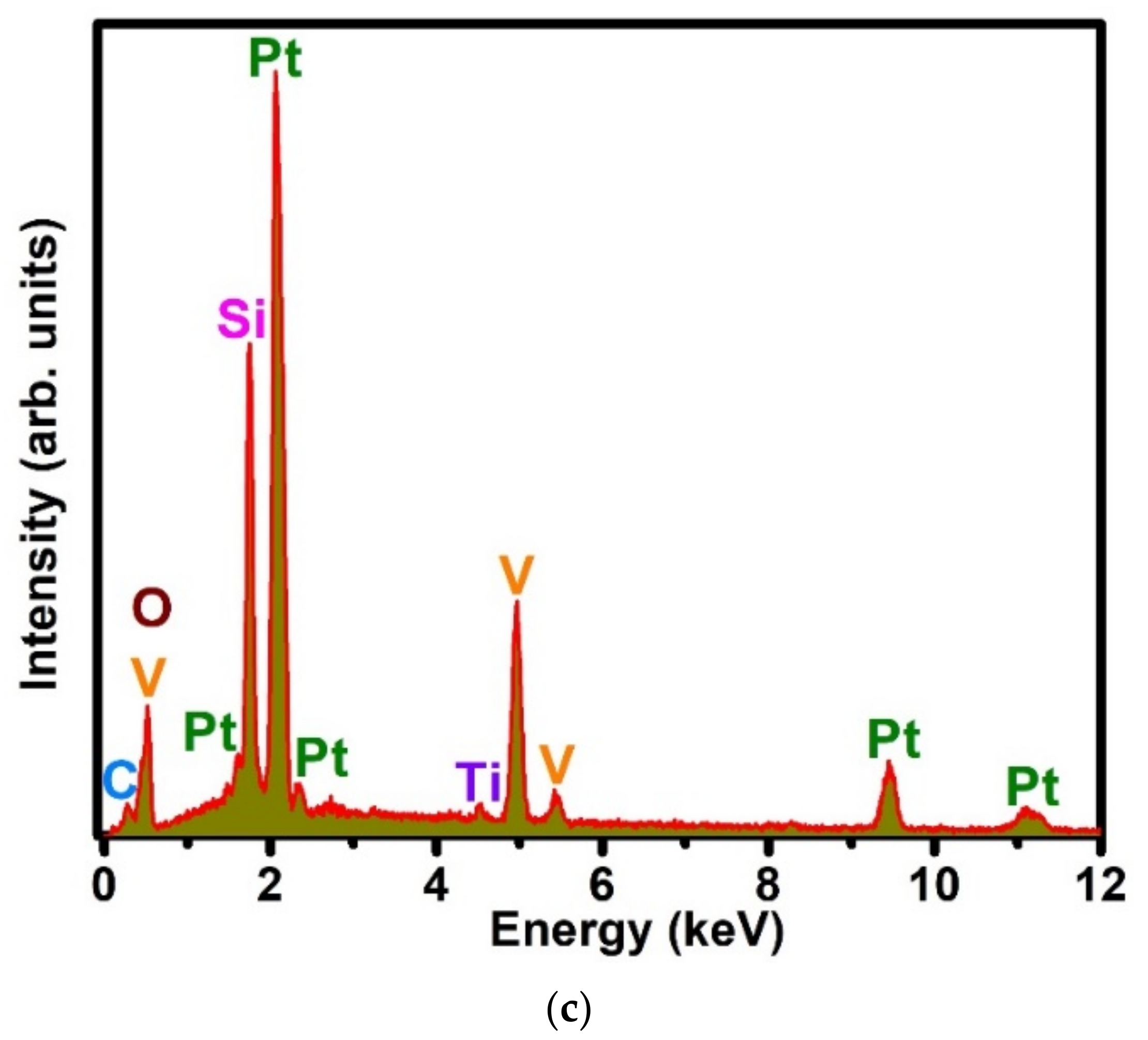
3. Results and Discussion

The single-phase formation of the as grown thin films was examined by X-ray diffraction (XRD) measurement.
Figure 1 shows the XRD pattern of the thin films measured in the 2θ range from 20–65°. The diffraction peaks were found to match with the V2O3 rhombohedral R 3 ¯ C structure (JCPDF # 340187) along with the reflection peaks of the Pt substrate located at 39.88° and 46.41°. The main X-ray reflection peaks from the compound were observed at 2θ positions of 24.44°, 33.34°, 36.43°, 41.32°, 50.09°, 54.21°, and 58.72°, those were corresponded to the lattice planes (012), (104), (110), (113), (024), (116) and (122), respectively, of the R 3 ¯ C phase, indicating the formation of the polycrystalline V2O3 thin film. In addition, the absence of any impurity peak in the diffraction pattern, suggesting the formation of a phase pure V2O3 thin film. The lattice mismatch between the grown thin film and the Pt-substrate may introduce a lattice strain (η) on the thin film. The strain can be calculated using the relation [21,22], η = (abulk−afilm/abulk) × 100. The XRD patterns from the substrate (2θ = 39.825°) and the film (2θ = 39.877°) have Pt (111) peaks. The tensile lattice strain can be obtained by using these peaks as a reference. Pt stabilize in cubic phase with their estimated lattice parameters turn out to be abulk = 3.920(1) Å, afilm = 3.915(2) Å, that yields a negligible strain of 0.13% in the thin film. The profilometer curve, scanned across bottom platinum step to the surface of the thin films, indicates that the thickness of the films is about 230 nm (Figure 1b).
Figure 2a shows the surface morphology of the thin films measured on a surface area of 5 μm × 5 μm using AFM microscopy. The surface of the thin film is found to be smooth with uniformly distributed grains with a surface roughness RQ of around 8.73 nm. The SEM image (Figure 2b) recorded from the film surface indicated a crack free smooth surface of the film. The homogeneous distribution of constituent chemical elements was evident from the EDS-elemental mapping measured on the thin film’s surface (Figure 2c). The EDS spectrum analysis revealed that the thin film is made up of multiple components of the crystal V2O3 phase and the amorphous carbon phase. The chemical oxidation states of the constituent elements V and O of the thin films were further examined by XPS. The XPS survey spectrum of the films grown on Si/SiO2/Ti/Pt substrates is depicted in Figure 3a. The peaks identified in the spectrum correspond to elements V, O, and C, and no impurity peaks were seen. The adventitious carbon C1s peak is observed due to the exposure of the sample to the environment. The binding energy (BE) 284.8 eV of this carbon C 1s peak was used as the BE scale reference. The high resolution XPS spectrum for the core level V2p and O1s states is shown in Figure 3b, in which the binding energies of the peaks of V2p3/2, V2p1/2, and O1s are basic representative of the oxidation state of VOx. The XPS spectrum was analyzed using a Shirley background to obtain the oxidation state of V and O ions (Table 1), and that indicated that the fitted peak position energy values of the characteristic XPS peaks match well with the literature [23,24]. It can be mentioned that a relatively large intensity of Carbon C1s peak is observed in the XPS survey spectrum, that could be probably due to contributions from two sources: a detectable quantity of adventitious carbon contamination due to exposer of the sample to the atmosphere, and from the double-sided carbon-tape normally that was used to fix a tiny thin film on the sample holder. The oxygen binding energy of the core level O1s is 531.677 eV [23], which is the standard energy reference for vanadium oxide as the ratio between oxygen (NO) and vanadium (NV) concentration NO/NV does not depict the differentiation between different oxide state [23]. The doublet of V2p corresponds to 2p3/2 and 2p1/2, resulted due to spin orbit coupling effect, are found to center around 515.863 and 523.075 eV. The energy difference Δ [= BE (V2p1/2) – BE (V2p3/2)] turns out to be 7.21 eV, a value close to the standard reference [23,25]. The difference in binding energy (ΔE) between V2p3/2 and O1s (531.67 eV) is 15.863 eV, confirming the presence of V on the surface of the film in V3+ oxidation state. Therefore, the oxidation states of vanadium and oxygen are inferred as V3+ and O2−, respectively [23,26], and that corroborates the growth of the V2O3 thin films.
DC magnetic hysteresis loop measurements were carried out at several temperature from 10–300 K in the applied magnetic field range of ±2 kOe (Figure 4). As can be seen, the magnetic order is found to change with increasing temperature. At a low temperature of 10 K (Figure 4a), the hysteresis loop is largely bifurcated with remnant magnetization MR = 5.23 emu/cm3 and coercive filed HC = 103.62 Oe. The bifurcation gap of the branches of the hysteresis curve becomes narrow upon increasing temperature and does not show any paramagnetic linear curve up to 300 K. For instance: at 100 K (Figure 4c), MR = 3.02 emu/cm3 and HC = 72.98 Oe, and at 300 K (Figure 4d), MR = 1.74 emu/cm3 and HC = 58.46 Oe were obtained. This evolution of magnetic ordering can be attributed to the slight ferrimagnetic polarization of mainly antiferromagnetic spins.
To identify the magnetic ordering phenomena, ZFC-FC magnetizations measurements were carried out at different magnetic fields. Figure 5 shows the ZFC and FC magnetization curves measured from the thin films at 100–1000 Oe. The ZFC and FC magnetization curves followed different paths up to applied field of 1000 Oe, that suggests that magnetization is related to the sample cooling history, which is typically observed in other magnetic systems [27,28]. These magnetization curves showed a small kink around 55 K at 100 Oe (Figure 5a) and that shifted to lower temperature at higher applied fields. The strong field dependence of that AFM transition is suggestive for a canted AFM transition and/or spin-glass-like magnetic ordering, which is similar to the magnetic ordering that reported in the bixbyite-type V2O3 bulk sample [11].
The temperature dependent behavior of the remanent MR and coercive field HC of the hysteresis loops measured at several temperatures is depicted in Figure 6. Both the remanent MR and the coercive field HC were found to decrease with increasing temperature as expected due to thermal spin disorder [27], and they exhibited an anomaly near 55 K. This anomaly can be attributed to a canted antiferromagnetic phase transition, in accord with the field dependence of kink anomaly temperature observed in the ZFC and FC magnetization curves.
As mentioned earlier, at room temperature, V2O3 crystallizes into a rhombohedral corundum-type phase, that belongs to R 3 ¯ C space group symmetry with the D3d point group [10]. Seven Raman active phonons (2A1g + 5Eg) are expected [10] in the room temperature phase. Theoretically, the Raman modes of monoclinic C2h phase at low temperature are [10]: 7Ag + 8Bg. Hence, 15 Raman active optical phonons are expected. The Raman spectrum measured at room temperature in the frequency range of 50–980 cm−1 is shown in Figure 7, that matches well with the earlier report [10]. Following the standard curve fitting procedure [29], the spectrum was analyzed using the Lorentzian function to obtain their Raman band frequencies (Figure 7). A minimum number of peaks were considered to fit the experimental data. The Raman mode at 220 cm−1 and 500 cm−1 can be assigned to the A1g mode, and the mode at 681 cm−1 can be assigned to the B1g mode of the rhombohedral phase [10,18].
A few modes are observed than the actual predicted one, probably due to insufficient intensities arising from the less polarizability of several phonons. Table 2 shows the frequency of observed Raman modes in the rhombohedral and monoclinic phases. The temperature dependent Raman spectra are shown in Figure 8. The Raman spectra exhibit changes upon passing through the monoclinic-rhombohedral phase transition in the temperature range from 82 to 300 K. At 82 K, the phonon modes were observed at 200 cm−1, 249 cm−1, and 500 cm−1, those are attributed to Ag phonon of the low temperature monoclinic phase [10]. The intensity of the Ag mode at 203 cm−1 reduces monotonically and disappears around 143 K. This observation suggests that the phase transition from mono-rhombohedral phase at 143 K, in accord with the earlier report on bulk V2O3 [10]. However, no signature of phase coexistence was observed in our study in contrast to that reported in V2O3 thin films [18]. This could be due to relaxation of stress in the present thin films of thickness around 230 nm as compared to reported thin films of 90 nm thickness that associated with significant stress and microstructural defects. The dependencies of mode frequency on temperature, obtained from curve fittings, are shown in Figure 9. The mode at 250 and 502 cm−1 continue to exist up to 300 K, while the 203 cm−1 mode disappeared at 143 K, the transition temperature. The temperature coefficient (dω/dT) of the modes in monoclinic phase is found larger than that in the rhombohedral phase (Table 2). This indicates that the monoclinic phase has higher anharmonicity. It can be mentioned that MIT of the V2O3 thin films occurs above 143 K, as reported in the temperature-dependent studies on electrical conductivity [15,30].
In the recent studies of the thickness dependence of V2O3 thin films [19,31], it was found that the electronic phase transition behaviors are strongly dependent on the film thickness and could also induce a metal-insulator transition, around the temperature-induced phase transition temperature.

4. Conclusions

V2O3 thin films were synthesized using a DC magnetic sputtering technique. At room temperature, the films were stabilized at a rhombohedral R 3 ¯ C phase. EDX and XPS studies indicated presence of nearly stochiometric chemical elements in the thin films. High resolution XPS studies indicated the binding energy of O1s is 531.677 eV, and that for 2p1/2 and 2p3/2 chemical states of vanadium are 523.075 eV and 515.863 eV, respectively. In phonon spectroscopic studies, A1g phonon modes at 220, 500 cm−1, and B1g mode at 681 cm−1 were observed at ambient temperature. Temperature-dependent Raman studies indicated a low temperature monoclinic to room temperature rhombohedral phase transition around ~143 K. Temperature dependent magnetization studies suggested a canted antiferromagnetic phase transition around ~55 K in low temperature.

Author Contributions

Data curation, I.C.; Formal analysis, K.K.M.; Funding acquisition, R.S.K.; Investigation, I.C.; Supervision, R.S.K.; Validation, K.K.M.; Writing—original draft, I.C.; Writing—review & editing, K.K.M. All authors have read and agreed to the published version of the manuscript.

Funding

This work was supported in part by the Department of Defence, USA (DoD Grant #FA9550-20-1-0064).

Institutional Review Board Statement

Not applicable.

Informed Consent Statement

Not applicable.

Data Availability Statement

Reasonable request to corresponding author at karunaphy05@gmail.com (K.K.M.).

Acknowledgments

We acknowledge financial support from the Department of Defense, USA (DoD Grant #FA9550-20-1-0064). We thank Molecular Science Research Centre and Speclab Research Facilities at the University of Puerto Rico for experimental research facilities.

Conflicts of Interest

The authors declare no competing financial interests.

References

  1. Haber, J. Fifty years of my romance with vanadium oxide catalysts. Catal. Today 2009, 142, 100–113. [Google Scholar] [CrossRef]
  2. Hess, C. Nanostructured Vanadium Oxide Model Catalysts for Selective Oxidation Reactions. ChemPhysChem 2009, 10, 319–326. [Google Scholar] [CrossRef] [PubMed]
  3. Prosini, P.P.; Xia, Y.; Fujieda, T.; Vellone, R.; Shikano, M.; Sakai, T. Performance and capacity fade of V2O5-lithium polymer batteries at a moderate-low temperature. Electrochim. Acta 2001, 46, 2623–2629. [Google Scholar] [CrossRef]
  4. Liu, P.; Lee, S.H.; Cheong, H.M.; Tracy, C.E.; Pitts, J.R.; Smith, R.D. Stable Pd/V2O5 Optical H2 Sensor. J. Electrochem. Soc. 2002, 149, H76–H80. [Google Scholar] [CrossRef]
  5. Muster, J.; Kim, G.T.; Krstić, V.; Park, J.G.; Park, Y.W.; Roth, S.; Burghard, M. Electrical Transport Through Individual Vanadium Pentoxide Nanowires. Adv. Mater. 2000, 12, 420–424. [Google Scholar] [CrossRef]
  6. Held, K.; Keller, G.; Eyert, V.; Vollhardt, D.; Anisimov, V.I. Mott-Hubbard metal-insulator transition in paramagnetic V2O3: An LDA + DMFT (QMC) study. Phys. Rev. Lett. 2001, 86, 5345–5348. [Google Scholar] [CrossRef] [Green Version]
  7. Luo, Q.; Guo, Q.; Wang, E.G. Thickness-dependent metal-insulator transition in V2O3 ultrathin films. Appl. Phys. Lett. 2004, 84, 2337–2339. [Google Scholar] [CrossRef]
  8. Sundar, C.S.; Bharathi, A.; Premila, M.; Hariharan, Y. Metal-insulator transition in V2O3: Positron lifetime studies. J. Alloys Compd. 2001, 326, 105–107. [Google Scholar] [CrossRef]
  9. Orowan, E. Quantum phase transitions. Rep. Prog. Phys. 2003, 66, 2069–2110. [Google Scholar]
  10. Kuroda, N.; Fan, H.Y. Raman scattering and phase transitions of V2O3. Phys. Rev. B 1977, 16, 5003–5008. [Google Scholar] [CrossRef]
  11. Weber, D.; Stork, A.; Nakhal, S.; Wessel, C.; Reimann, C.; Hermes, W.; Müller, A.; Ressler, T.; Pöttgen, R.; Bredow, T.; et al. Bixbyite-Type V2O3—A Metastable Polymorph of Vanadium Sesquioxide. Inorg. Chem. 2011, 50, 6762–6766. [Google Scholar] [CrossRef] [PubMed]
  12. Rao, C.N.R.; Raveau, B. Transition Metal Oxide: Structure, properties and Synthesis of Ceramic Oxide. Organometal. Chem. 1999, 13, 475–480. [Google Scholar]
  13. Yang, Z.; Ko, C.; Ramanathan, S. Oxide electronics utilizing ultrafast metal-insulator transitions. Annu. Rev. Mater. Res. 2011, 41, 337–367. [Google Scholar] [CrossRef]
  14. Chen, X.B.; Kong, M.H.; Choi, J.Y.; Kim, H.T. Raman spectroscopy studies of spin-wave in V2O3 thin films. J. Phys. D Appl. Phys. 2016, 49, 465304. [Google Scholar] [CrossRef]
  15. Allimi, B.S.; Alpay, S.P.; Xie, C.K.; Wells, B.O.; Budnick, J.I.; Pease, D.M. Resistivity of V2O3 thin films deposited on a-plane (110) and c-plane (001) sapphire by pulsed laser deposition. Appl. Phys. Lett. 2008, 92, 202105. [Google Scholar] [CrossRef] [Green Version]
  16. Allimi, B.; Alpay, S.; Goberman, D.; Huang, T.; Budnick, J.; Pease, D.; Frenkel, A. Growth of V2O3 thin films on a-plane (110) and c-plane (001) sapphire via pulsed-laser deposition. J. Mater. Res. 2007, 22, 2825–2831. [Google Scholar] [CrossRef]
  17. Misochko, O.V.; Tani, M.; Sakai, K.; Kisoda, K.; Nakashima, S.; Andreev, V.N.; Chudnovsky, F.A. Optical study of the Mott transition in V2O3: Comparison of time-and frequency-domain results. Phys. Rev. B 1998, 58, 12789–12794. [Google Scholar] [CrossRef]
  18. Chen, X.B.; Shin, J.H.; Kim, H.T.; Lim, Y.S. Raman analyses of co-phasing and hysteresis behaviors in V2O3 thin film. J. Raman Spectrosc. 2012, 43, 2025–2028. [Google Scholar] [CrossRef]
  19. Allimi, B.S.; Aindow, M.; Alpay, S.P. Thickness dependence of electronic phase transitions in epitaxial V2O3 films on (0001) LiTaO3. Appl. Phys. Lett. 2008, 93, 112109. [Google Scholar] [CrossRef] [Green Version]
  20. Brockman, J.; Aetukuri, N.P.; Topuria, T.; Samant, M.G.; Roche, K.P.; Parkin, S.S.P. Increased metal-insulator transition temperature in epitaxial thin films of V2O3 prepared in reduced oxygen environments. Appl. Phys. Lett. 2021, 98, 152105. [Google Scholar] [CrossRef]
  21. Bhattarai, M.K.; Mishra, K.K.; Instan, A.A.; Bastakoti, B.P.; Katiyar, R.S. Enhanced energy storage density in Sc3+ substituted Pb(Zr0.53Ti0.47)O3 nanoscale films by pulse laser deposition technique. Appl. Surf. Sci. 2019, 490, 451. [Google Scholar] [CrossRef]
  22. Sanchez, D.A.; Kumar, A.; Ortega, N.; Katiyar, R.S.; Scott, J.F. Near-room temperature relaxor multiferroic. Appl. Phys. Lett. 2010, 97, 202910. [Google Scholar] [CrossRef]
  23. Hryha, E.; Rutqvist, E.; Nyborg, L. Stoichiometric vanadium oxides studied by XPS. Surf. Interface Anal. 2012, 44, 1022–1025. [Google Scholar] [CrossRef]
  24. Bocquet, A.E.; Mizokawa, T.; Morikawa, K.; Fujimori, A.; Barman, S.R.; Maiti, K.; Sarma, D.D.; Tokura, Y.; Onoda, M. Electronic structure of early 3d-transition-metal oxides by analysis of the 2p core-level photoemission spectra. Phys. Rev. B 1996, 53, 1161–1170. [Google Scholar] [CrossRef]
  25. Mendialdua, J.; Casanova, R.; Barbaux, Y. XPS studies of V2O5, V6O13, VO2 and V2O3. J. Electron Spectrosc. Relat. Phenom. 1995, 71, 249–261. [Google Scholar] [CrossRef]
  26. Zimmermann, R.; Claessen, R.; Reinert, F.; Steiner, P.; Hüfner, S. Strong hybridization in vanadium oxides: Evidence from photoemission and absorption spectroscopy. J. Phys. Condens. Matter 1998, 10, 5697–5716. [Google Scholar] [CrossRef]
  27. Mishra, K.K.; Satya, A.T.; Bharathi, A.; Sivasubramanian, V.; Murthy, V.R.K.; Arora, A.K. Vibrational, magnetic, and dielectric behavior of La-substituted BiFeO3-PbTiO3. J. Appl. Phys. 2011, 110, 123529. [Google Scholar] [CrossRef]
  28. Mishra, K.K.; Hernandez, J.A.; Instan, A.A.; McCartan, S.J.; Marty Gregg, J.; Katiyar, R.S. Lead palladium zirconate titanate: A room temperature nanoscale multiferroic thin film. J. Appl. Phys. 2020, 127, 204104. [Google Scholar] [CrossRef]
  29. Mishra, K.K.; Arora, A.K.; Tripathy, S.N.; Pradhan, D. Dielectric and polarized Raman spectroscopic studies on 0.85Pb(Zn1/3Nb2/3)O3−0.15PbTiO3 single crystal. J. Appl. Phys. 2012, 112, 073521. [Google Scholar] [CrossRef]
  30. Homm, P.; Menghini, M.; Seo, J.W.; Peters, S.; Locquet, J.P. Room temperature Mott metal-insulator transition in V2O3 compounds induced via strain-engineering. APL Mater. 2021, 9, 21116. [Google Scholar] [CrossRef]
  31. Grygiel, C.; Simon, C.; Mercey, B.; Prellier, W.; Frésard, R.; Limelette, P. Thickness dependence of the electronic properties in V2O3 thin films. Appl. Phys. Lett. 2007, 91, 262103. [Google Scholar] [CrossRef] [Green Version]
Scheme 1. Schematic diagram for growth of V2O3 thin film.
Coatings 12 00649 sch001
Figure 1. (a) X-ray diffraction pattern of the Si/SiO2/Ti/Pt substrates and V2O3 thin films grown on the substrates; (b) a profilometer-based scanned profile of the thin films’ surface indicates that the thickness of the films are ~230 nm.
Coatings 12 00649 g001
Figure 2. (a) AFM micrograph of a V2O3 film at 100 nm in Z-scale (Inset: 3D AFM image) (b) SEM micrograph and distribution maps of elements V and O, as well as their sum total mapping of surface area (c) EDS spectrum of theV2O3 thin films shows the presence of all constituent elements at their respective characteristic energy level.
Coatings 12 00649 g002aCoatings 12 00649 g002b
Figure 3. (a) Survey XPS spectrum and (b) analysis of high resolution XPS peaks in V2O3 thin films corresponding to vanadium and oxygen elements.
Coatings 12 00649 g003
Figure 4. Magnetization vs. magnetic field of V2O3 thin films measured at different temperatures (a) 10 K; (b) 55 K; (c) 100 K; (d) 300 K.
Coatings 12 00649 g004
Figure 5. ZFC & FC magnetization curves measured on V2O3 films at different applied magnetic fields. (a) 100 Oe; (b) 500 Oe; (c) 1000 Oe.
Coatings 12 00649 g005
Figure 6. Temperature dependencies of remanent magnetization (MR) and coercive field (HC) of hysteresis curves of V2O3 thin films.
Coatings 12 00649 g006
Figure 7. Raman spectrum measured at room temperature in the frequency range of 50–980 cm−1. The total fitted and individual components of the spectrum are also shown separately.
Coatings 12 00649 g007
Figure 8. Raman spectra recorded at different temperatures. The total fitted and individual components of the spectrum are also shown separately.
Coatings 12 00649 g008
Figure 9. Mode frequency dependence of the A1g phonon mode as a function of temperature. The vertical line represents the crystal phase transition temperature Tc around 143 K.
Coatings 12 00649 g009
Table 1. XPS spectral parameters of the deconvoluted peaks for sesquioxide vanadium.
ElementChemical StatePeak Position (eV)
OO1s531.677
V2p1/2523.075
2p3/2515.863
Table 2. Here, one can see the Raman mode frequencies and temperature coefficients in various phases of the V2O3 thin films. The number in the parenthesis indicates the standard error in the least significant digit.
Monoclinic Phase (B2/b) Rhombohedral   Phase   ( R 3 ¯ C )
Modeω (cm−1)
T = 82 K
dω/dT
(cm−1/K)
Modeω (cm−1)
T = 143 K
dω/dT
(cm−1/K)
Ag203−0.009(6)---
Ag250−0.038(5)A1g247−0.040(1)
Ag502−0.051(6)A1g499−0.009(5)
Publisher’s Note: MDPI stays neutral with regard to jurisdictional claims in published maps and institutional affiliations.

