Article

Molecular Dynamics Simulation of Chip Morphology in Nanogrinding of Monocrystalline Nickel

School of Mechanical and Electronical Engineering, Lanzhou University of Technology, Lanzhou 730050, China
*
Author to whom correspondence should be addressed.
Coatings 2022, 12(5), 647; https://doi.org/10.3390/coatings12050647
Submission received: 13 March 2022 / Revised: 12 April 2022 / Accepted: 5 May 2022 / Published: 9 May 2022
(This article belongs to the Special Issue 10th Anniversary of Coatings: Invited Papers in Tribology Section)

Abstract

:
In this study, the nanogrinding process for single-crystal nickel was investigated using a molecular dynamics simulation. A series of simulations were conducted with different tool radii and grinding methods to explore the effects of chip morphology, friction forces, subsurface damage, and defect evolution on the nanogrinding process. The results demonstrate that the workpiece atoms at the back of the tool were affected by the forward stretching and upward elastic recovery when no chips were produced. Although the machining depth was the smallest, the normal force was the largest, and dislocation entanglement was formed. The small number of defect atoms indicates that the extent of subsurface damage was minimal. Moreover, when spherical chips were produced, a typical columnar defect was generated. The displacement vector of the chip atoms aligned with the machining direction and as the chips were removed by extrusion, the crystal structure of the chip atoms disintegrated, resulting in severe subsurface damage. By contrast, when strip chips were produced, the displacement vector of the chip atoms deviated from the substrate, dislocation blocks were formed at the initial stage of machining, and the rebound-to-depth ratio of the machined surface was the smallest.

1. Introduction

Nickel-based single-crystal materials have been widely used in aviation applications, aerospace engines, gas turbines, and other national defense industrial equipment owing to their excellent high-temperature resistance, oxidation resistance, and thermal fatigue properties. With the increasing demand for the development of specialized parts, nanogrinding technology has developed rapidly and has come to symbolize the technical advancement of a country [1,2,3]. However, hardening often occurs during the machining of single-crystal nickel, leading to increased surface roughness and subsurface damage [4]. This determines the performance of the structural components of the aeroengine. In the physical cutting process, the machining of different tools leads to different degrees of hardening, which causes many unnecessary problems in the subsequent machining process [5,6]. Moreover, when the machining accuracy reaches the nanometer level, the continuous medium theory is unsuitable for explaining the nanogrinding mechanism [7,8,9]. Furthermore, atomic transient changes cannot be observed accurately or effectively using nanogrinding experiments using existing machining technology. Therefore, molecular dynamics simulation has become an important tool for nanogrinding research [10,11].
Previous studies on the nanogrinding of single-crystal materials using molecular dynamics have mostly focused on copper and silicon [8,12,13]. With the development of molecular dynamics simulation research, machining objects have been extended to titanium, nickel, and other important single-crystal aerospace materials [14,15]. It is an important component of nickel-based single-crystal blades and plays a key role in aerospace applications. In this study, single-crystal nickel, which is the component material of the γ-matrix in nickel-based single-crystal blades, was used as the research object. As both single-crystal copper and nickel are FCC crystals, the research based on single-crystal copper provided insight for this study [7,16]. Karkalos et al. [17] investigated cases of nanogrinding workpieces of three different fcc metals, namely, copper, nickel, and aluminum, under different preheating temperatures to determine the efficiency of the hot nanogrinding technique. Huang et al. [18] found, by comparing the nanogrinding simulation results of single-crystal copper and aluminum, that the plastic deformation of two materials was caused by the nucleation and movement of dislocations. Fang et al. [19] studied the effects of different machining parameters on the subsurface damage and material removal of Ni/Cu multilayers using molecular dynamics. Eder et al. [20] used large-scale molecular dynamics simulations to study the effect of temperature on the deformation response of FCC CuNi alloys of various compositions under various normal pressures. Hao et al. [21] studied the diffusion mechanism of machining tools using molecular dynamics. Wang et al. [22] studied the evolution of subsurface defect structures in the process of single-crystal copper nanogrinding and found ladder rod dislocations, stacking-fault tetrahedrons, atomic defect clusters, and vacancy defects in the subsurface. Wang et al. [23] investigated the effect of cutting speed and depth on the deformation behavior of single-crystal GaN. Xu et al. [24] studied the nanogrinding process of copper–silicon at different speeds and depths. Previous studies have not focused on chip morphology differences and their root cause, and consequently, there is a lack of research on the material flow law and chip generation mechanism under different chip forms in nanogrinding.
In this study, the law of atomic motion, chip morphology, atomic kinetic energy distribution, characteristics of the machining force, internal crystal structure, typical defects, evolution of defects, and subsurface quality when different forms of chips were generated were studied. The chip formation mechanism for different chip forms was described. The findings of this study can serve as a good foundation for understanding the machining and deformation mechanisms of nickel-based single-crystal parts.

2. Modeling and Simulation Details

In this study, a molecular dynamics simulation model of a nickel-based single crystal composed of a single-crystal nickel matrix and a diamond tool is presented. The workpiece and tool models were established using the LAMMPS simulation software [25,26]. The workpiece material was a nickel single-crystal model with a face-centered cubic lattice structure with the lattice constant determined as 0.352 nm. During the friction process, the tool performed linear contact motion. It was assumed that the tool wear behavior in the friction process could be ignored and that the elastic–plastic deformation of the matrix was uniform.
Figure 1 shows the molecular dynamics simulation model of single-crystal nickel nanogrinding at the different tool radii. The dimensions of the workpiece were 58 × 24 × 7.5 nm3, which included 807,080 atoms; the diamond cutter contained 57,661 carbon atoms. In addition, periodic boundary conditions were applied on the workpiece in the Z direction, and aperiodic boundary conditions were applied in other directions during the simulation.
To achieve cutting, a constant machining speed and backdraft were used in the simulation. Fixed, constant temperature, and Newton layer assumptions were used for the workpiece and tool. The fixed layer supported the entire workpiece and prevented it from moving during friction [27]. The yellow atom between the fixed layer and the substrate was the constant temperature layer, which adopted the Berendsen thermal bath method [28]. The temperature was maintained at 300 K by periodically adjusting the atomic velocity to keep the temperature at approximately ambient temperature. The blue and green atoms represent Newton layer atoms. The key research objective was to observe the processing deformation and damage of materials. Both the constant temperature and Newton layer motion followed Newton’s second law and were determined by the direct integration of the classical Hamiltonian equations of motion using the velocity–Verlet method [29,30]. Compared with previous simulation models, the size of the model used in this study was large enough to eliminate the influence of the size effect on the simulation results [31,32,33,34]. The MD simulation parameters of nano machining are shown in Table 1.
The embedded atom method (EAM) potential was adopted to describe the atomic interactions in Ni–Ni. The formula used is as follows [35,36,37,38]:
E t o t = i F i ρ i + 1 2 i , j i j φ i j R i j φ ,
where ρi is the electron density at each atomic location, Fi is the embedding energy function, and φ i j is the action-coupled potential between the two nuclei.
The interaction between tool atoms is described by the Tersoff potential. The formula is as follows [39]:
E = i E i = 1 2 E i = 1 2 i j V i j ,
where E is the binding energy; E i is the contribution of the ith atom in the system to the binding energy of the system; and V i j is affected by the local environment where the ith atom is located.
The interaction between the tool and workpiece atoms is described by the Morse potential. The expression is as follows [24,40]:
E i = i j D e 2 α r i j r 0 2 e 2 α r i j r 0 ,
where α is the potential energy curve gradient coefficient, D is the binding energy, and r0 is the interatomic distance when the force is zero. The correlation parameter of the Morse potential function between the C–Ni atoms is as follows: De = 0.100 eV, α = 2.2 Å−1, re = 2.4 Å [41].

3. Simulation Results and Discussion

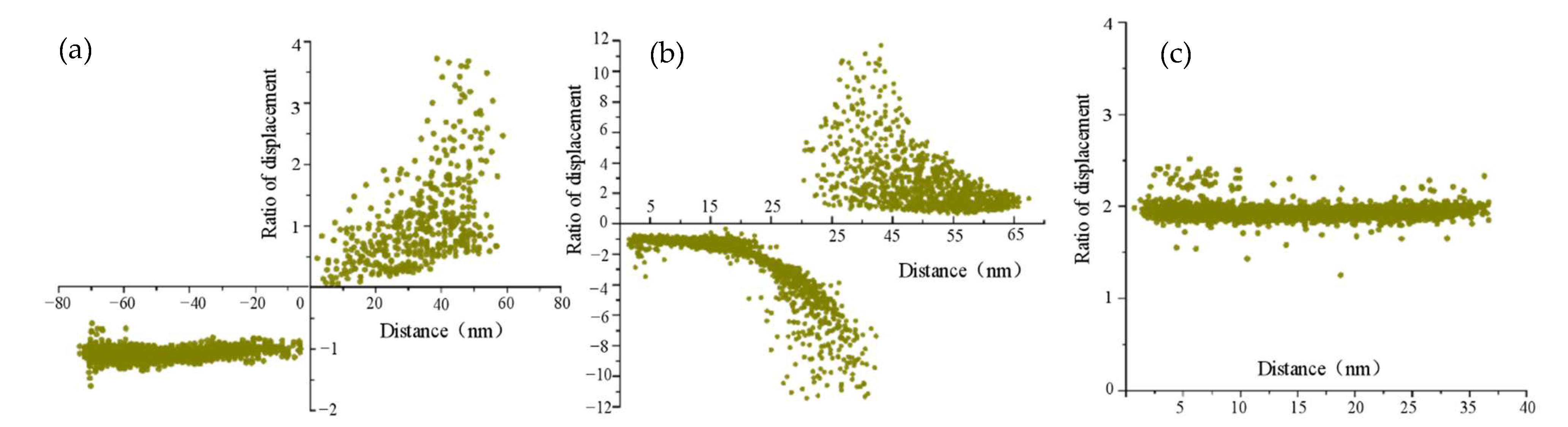
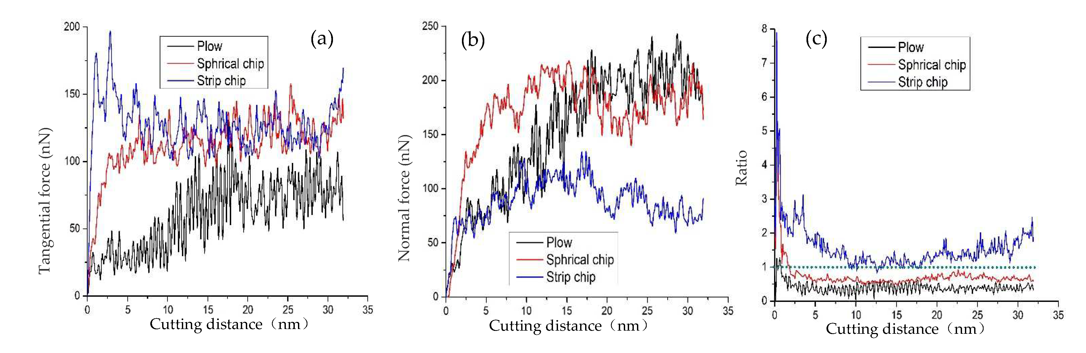
3.1. Atomic Displacement and Machining Force at Different Machining States

Similar to conventional machining, when the machining depth does not reach the minimum machining nanothickness, the tool only plows the workpiece surface without continuous and stable chip generation. Chip generation occurs when the machining depth exceeds the minimum machining thickness [42]. However, it was found in this study that the chips showed different shapes with changes in the tool radius and machining depth, and there were significant differences in the effect of the action mode of the tool on the workpiece, defects inside the workpiece, and the physical state of the chip atoms when different chips were generated. Machining processes with tool radii of 0, 1.58, 3.24, and 4.62 nm and machining depths of 0.3, 0.5, 1, 1.5, 2, 3, and 4 nm were analyzed. Figure 2 shows the atomic displacement vectors of different chips generated by the atomic displacement vector method.
To accurately observe the displacement variation in the atoms at different depths of cut, the displacement vectors of each atom were displayed using the displacement vector command in OVITIO [43]. It was observed that no chips were produced when the tool radius was 1.58 nm and the machining depth was 0.3 nm, as shown in Figure 2a. The workpiece surface was plowed by the machining tool, the atoms in front of the cutter tip were squeezed, and the displacement vector of these atoms was downward, extending to the interior of the workpiece. This is shown in Figure 2a. The deformation of the workpiece atoms at the back of the tool tip was restored because of the departure of the tool. Simultaneously, the distance between the workpiece atoms at the back of the tool tip increased under the action of the tool. After synthesizing the deformation trends of these two parts, the workpiece atom at the back of the tool tip produced an upward displacement trend. The displacement vector of an atom is shown as B in Figure 2a.
When the tool radius was 1.58 nm and the machining depth was 0.5 nm, spherical chips were formed, as shown by b1 in Figure 2b. The displacement vector of the chip atoms radiated in the machining direction, which is related to the forward movement of spherical chips in the manner of stacking and rolling during machining. Strip chips were formed when the tool radius was 1.58 nm and the machining depth was 1.5 nm, as shown by b2 in Figure 2b. The displacement vector of the atoms in the chips was almost the same, the material was removed as a whole, and the chips were removed by shearing, which shows that an increase in machining depth leads to a change in the chip from spherical to strip-like. When the machining depth decreased to 1.0 nm and the tool radius changed from 4.62 nm to 0 nm, different chips were generated, as shown in Figure 2c. A tool radius of 4.62 nm, shown in c1, produced the spherical chip. However, the tool radius of 0 nm, shown in c2, produced the strip chip. This indicates that an increase in tool radius leads to a change in the chip from strip-like to spherical.
To investigate the movement of the workpiece and chip atoms in the machining process, the X and Y displacements of the workpiece atoms located on the left and right sides of the tool tip were extracted. A scatter diagram reflecting the atomic displacements under different processing conditions was obtained, as shown in Figure 3. The abscissa represents the distance between the workpiece atom and the tool tip. If the distance is negative, it indicates that the workpiece atom is on the left side of the tool tip. Conversely, a positive distance indicates that the workpiece atom is on the right side of the tool tip. The ordinate represents the ratio of Y and X displacements of the atoms.
When plowing, as indicated in Figure 3a, the displacement ratio of atoms on the left side of the tool was 1. This indicates that the angle between the displacement vector and machining direction was 45°, and the trajectories of atoms were in the slip system of a single crystal. The displacement ratio of the atoms on the right side of the tool was in the range of 0–4. The closer the atoms are to the tool, the smaller the ratio, which means that the forward stretching effect of the workpiece atoms was more evident, and the upward elastic recovery effect was weaker. As shown in Figure 3b, when spherical chips were produced, the displacement ratio of chip atoms was concentrated between −1 and 1. The chip rolled into a ball and so the displacement vector between adjacent atoms changed continuously. As shown in Figure 3c, the displacement ratio of the chip atoms was a fixed value when strip chips were generated. This suggests that the chips are removed in a general manner, and the value is related to the shape of the tool.
Figure 4 depicts the chip height and surface rebound under different cutting depths (with a tool radius of 1.58 nm) and different tool radii (with a cutting depth of 1 nm). As shown in Figure 4a, the chip height decreased with the increase in tool radius. With a cutting depth of 1.0 nm, the largest chip height was produced when the tool nose radius was 0 nm. With the increase in tool radius, the chip quickly became spherical, and the chip height decreased gradually. When the tool radius was 1.58 nm, the chip height enlarged with the increase in cutting depth, but the growth rate of the chip height varied in different stages. When the cutting depth increased from 0.5 nm to 1 nm, spherical chips were produced, and the chip height increased gradually. By contrast, the chip height increased sharply when the cutting depth ranged from 1 nm to 1.5 nm, and strip chips were generated. Subsequently, the chip heights increased gradually with increasing cutting depth.
Figure 4b shows that the rebound of the cut surface increased with the increase in the tool radius at the cutting depth of 1.0 nm, which is related to the extrusion degree of the workpiece due to the large tool radius. It led to a more serious extrusion and greater elastic recovery on the surface during chip formation. At a tool radius of 1.58 nm and an e cutting depth of 0.3 nm, no chips were generated. The surface of the workpiece experienced complete elastic deformation, and the surface rebound was at the maximum when the machining depth was 0.3 nm. With the increase in cutting depth, spherical chips were produced, and the surface rebound decreased rapidly. When strip chips were produced, the surface rebound increased slightly and remained stable. Therefore, this processing form is conducive to obtaining an ideal surface.
The changes in the tangential force, normal force, and ratio of the tangential force to the normal force in the aforementioned machining states were analyzed, as shown in Figure 5, wherein the friction coefficient is the ratio of the tangential force to the normal force. As shown in Figure 5a, the tangential forces in the three different states tended to stabilize after a rapid increase in the initial stage. When spherical chips and strip chips were produced, the tangential forces were large, the variation in these two forces was almost identical, and the tangential force in the plowing state was the smallest, which is because only a few atoms in the horizontal direction interacted with the tool. As shown in Figure 5b, after the forces stabilized, the normal force in the plowing state was the largest. The strip chip was the smallest, which was the opposite of the cutting depth in the three machining states. The results show that when plowing, the tool had the strongest destructive effect on the subsurface, and when strip chips were produced, the damage to the subsurface was the weakest, which was conducive to obtaining a better machined surface. The change in the ratio of the tangential force to the normal force in the three machining states is shown in Figure 5c. After stable machining, the ratio was less than 1 during plowing and ball chip generation. The downward extrusion effect of the tool on the workpiece atom was greater than the removal and stripping effects. When strip chips were produced, the ratio exceeded 1, which indicates that the primary function of the tool is material removal.

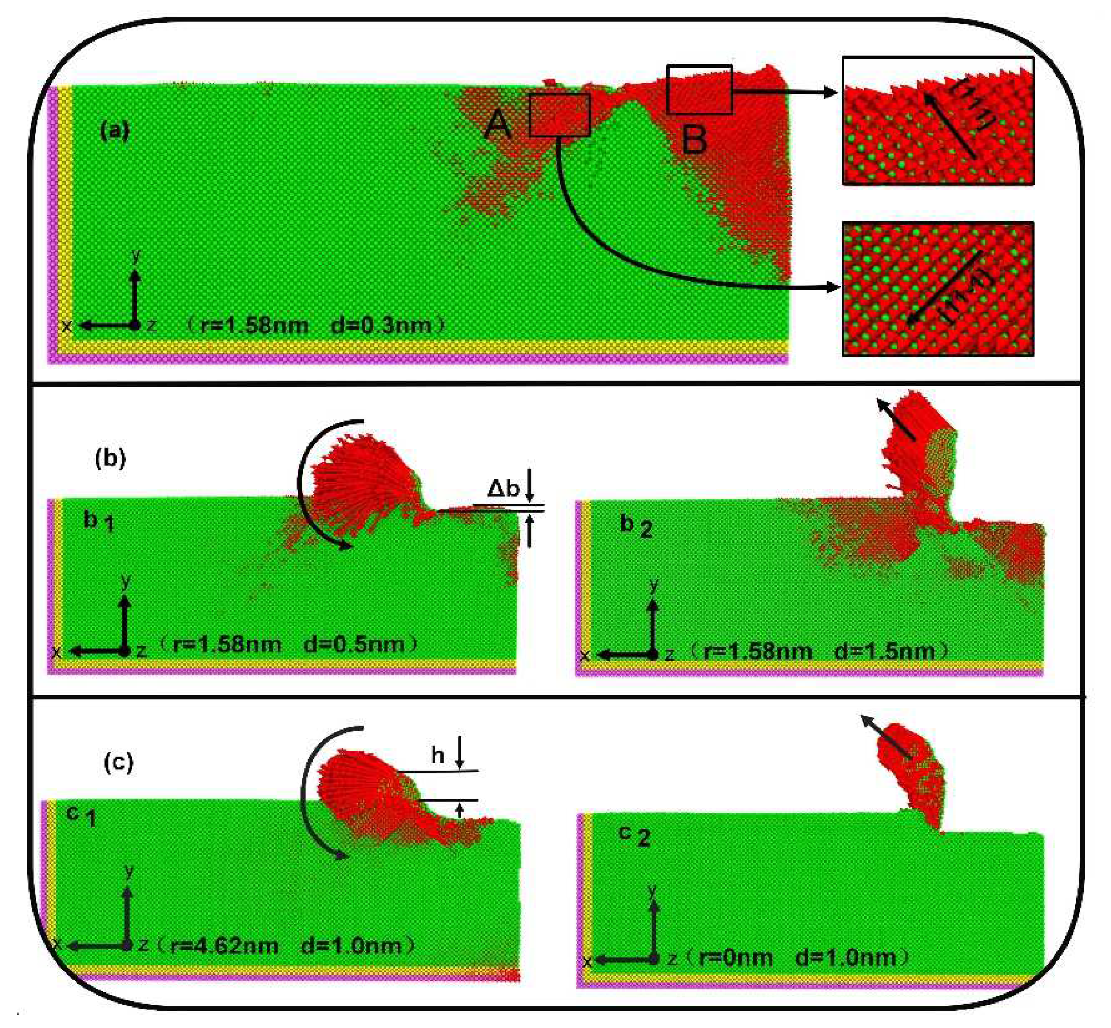
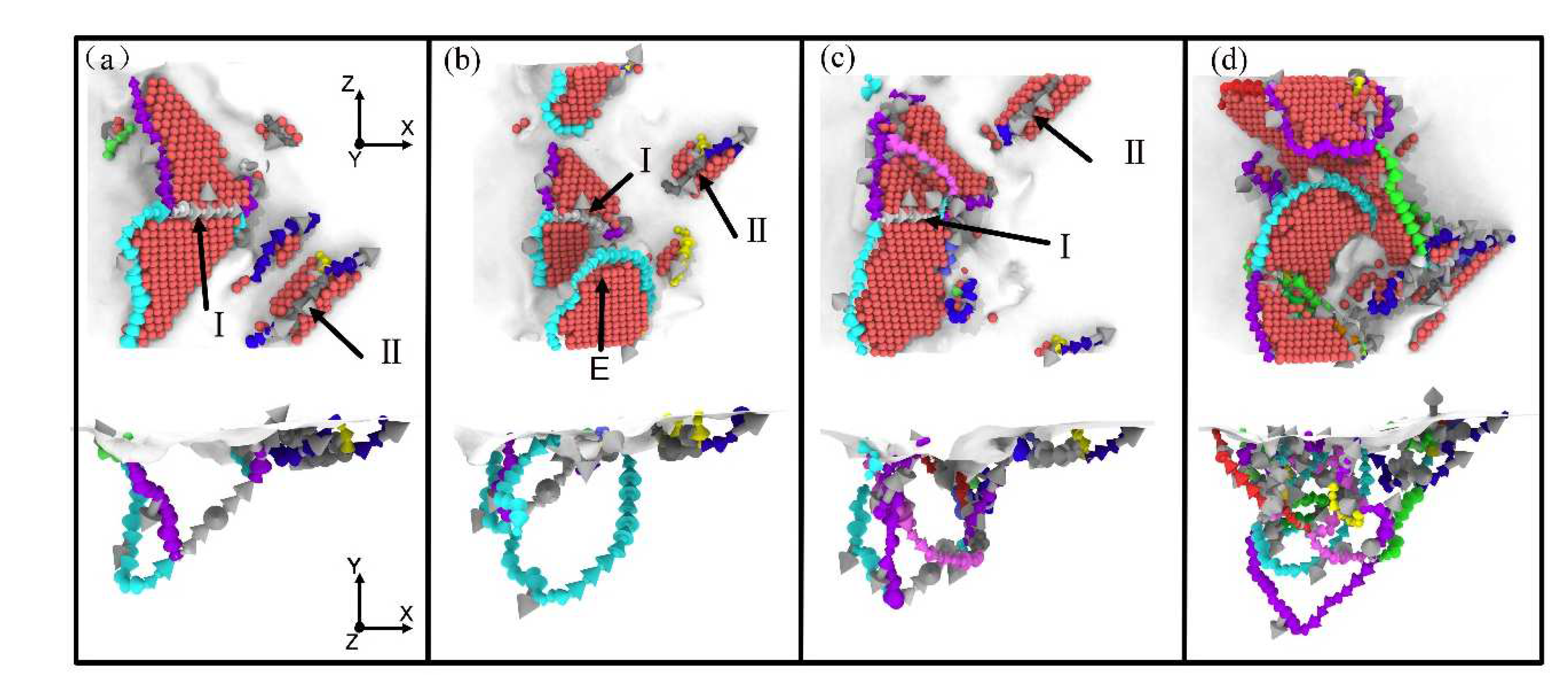
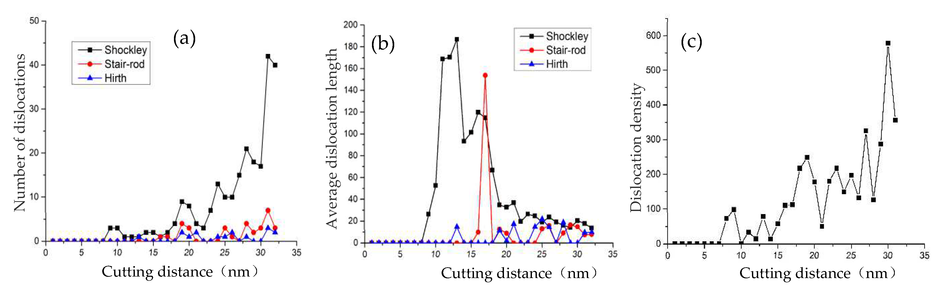
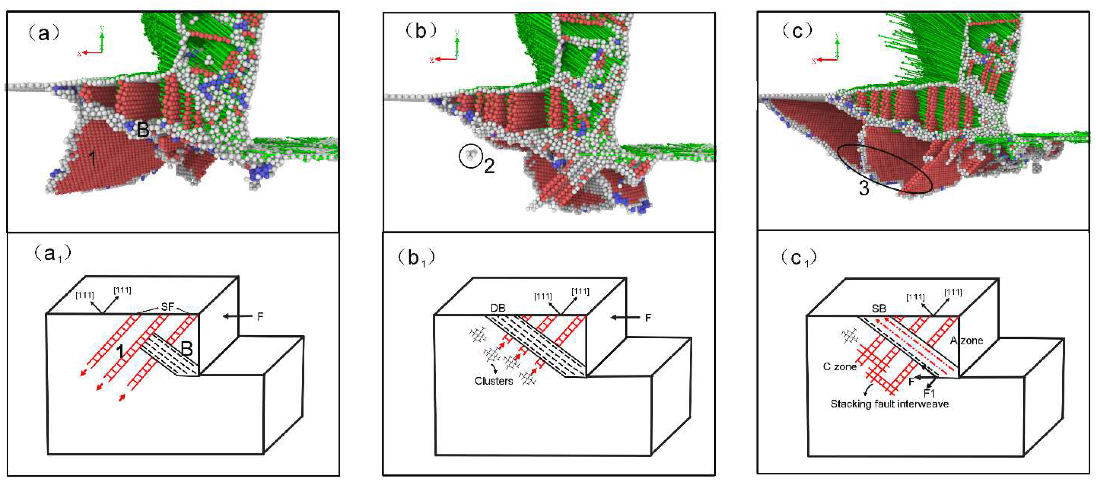
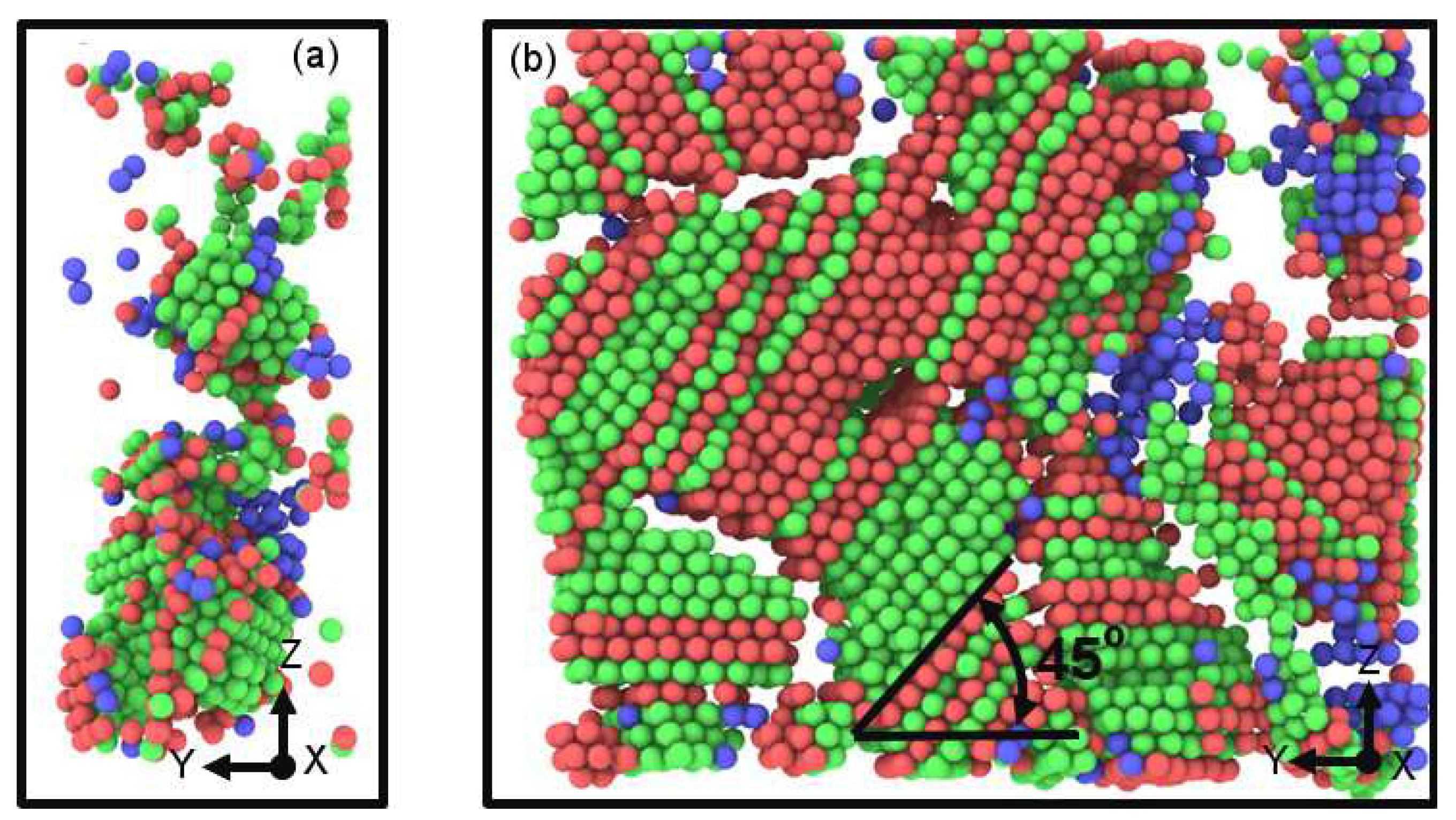
3.2. Internal Defects in Different Machining States

The common neighbor analysis (CNA) [44] method was used to analyze the internal crystal structure of the different machining states, as shown in Figure 6. To facilitate the analysis, the perfect FCC atoms in the crystals were removed. Red represents the HCP atoms, white represents the surface and amorphous atoms, and blue represents the BCC atoms. When plowing, the action range of the tool on the workpiece was limited, and the material was always in the early stage of plastic deformation; thus, a high-density region of dislocations was formed in the machining area [45]. The limited machining depth was not sufficient to form large defects in the high-density region of dislocations to absorb and destroy small dislocations. The small dislocations gradually increased and tangled with each other, finally forming a dislocation tangle [46], as illustrated by 1 in Figure 6a. After the tool left, the subsurface defects of the workpiece almost recovered, and only a few point defects remained, as demonstrated in Figure 6a, vacancy defect 2.
A V-shaped dislocation loop was generated in front of the tool when spherical chips were formed, as shown 1 in Figure 6b. Stacking-fault tetrahedrons and atomic clusters were present inside the machined surface, as shown by 2 and 3 in Figure 6b. Several types of defects were formed in this stage, indicating that subsurface damage is more severe when spherical chips are produced. This was primarily caused by the increase in machining depth and the removal of material by extrusion.
Figure 6c shows that when strip chips were produced, slip channel B was formed, which penetrated the workpiece surface. Atomic region A above the slip channel was removed in an overall manner, and the atoms in region A were composed of HCP and FCC atoms. The degree of damage to atoms in this region was relatively small. Because of the formation of the slip channel, the internal energy stored in the workpiece was released, so the number and volume of defects in zone C gradually decreased with machining, and only a few defect structures remained in the subsurface. It is worth noting that a sliding channel was generated when the strip chip was generated. At this time, the machining efficiency was high, and the tool wear was small.
To analyze the formation process of the dislocation tangle in detail, internal defects in the plowing state were analyzed when the machining distances were 12, 13, 14, and 20 nm using the dislocation extraction algorithm (DXA) [47], as depicted in Figure 7. Small L-C dislocations I and II formed on the subsurface when the machining distance was 12 nm, as displayed in Figure 7a. With the continuous input of cutting energy, the extended dislocation E around the L-C dislocation began to develop and increase, and the energy storage inside the crystal was partially released; therefore, the L-C dislocation I balanced the decrease in internal energy by reducing the volume, as seen in Figure 7b. Figure 7c shows that when the extended dislocation increased to a certain extent, it interacted with L-C dislocations I and II. Owing to the limited machining depth, there was no large defect structure with dominant deformation on the subsurface; therefore, L-C dislocations and extended dislocations repeated the interactive process. This resulted in a dislocation tangle, as shown in Figure 7d.
As displayed in Figure 8, the dislocation evolution during the formation of a dislocation tangle was quantitatively studied, and the change rules of the number, average length, and density of dislocations in the subsurface during machining were analyzed. It can be seen from Figure 8a that the number of dislocations increased with the machining distance, the number of Shockley partial dislocations was large, and the growth rate was fast. Conversely, the number of stair-rod and Hirth dislocations formed by the Shockley partial dislocations was relatively small. The length of the dislocations first increased and then decreased sharply, as shown in Figure 8b. This is because dislocations gradually develop and increase in length at the beginning of machining. However, because of the inability to form a large defect structure, dislocations such as Shockley interact with the stair-rod and Hirth dislocations and begin to decompose, so the length of dislocations decreases sharply. Based on an analysis of the dislocation density in the 4 × 4 nm2 region of the workpiece in front of the tool, it was found that the dislocation density in front of the tool increased gradually. Combined with the changes in Figure 8a,b, it can be concluded that a dislocation tangle occurs in the workpiece after plowing enters the stable stage, and the defects are characterized by large quantities and small volumes. As shown in Figure 8c, the dislocation density increased as the cutting distance increased.
As shown in Figure 9a, in the early stage of spherical chip formation, the distance between the workpiece atoms in front of the tool became increasingly smaller, leading to the destruction of the crystal structure to form an amorphous atomic layer S. As the tool continued to move forward, the amorphous atoms began to move relative to each other, and the atoms in direct contact with the tool were squeezed and began to flow to the workpiece surface. As the amorphous atoms accumulated in front of the tool and the tool continued to move, a large number of atoms accumulated in front of the tool, leading to an increase in the thickness of the amorphous atomic layer and a gradual shift from the action range of the cutting tool. Moreover, because of the weakening of the force and temperature, recovery began to occur in the amorphous atoms, forming a relatively concentrated crystal structure, A, as illustrated in Figure 9b.
As seen in Figure 9c, the crystalline structure A grew as the number of amorphous atoms and the distance from the tool increased. In addition, a laminar dislocation with a structure-strengthening effect was generated internally, which increased the strength of crystalline structure A and impeded the forward flow of amorphous atoms. The extruded and discrete flowing atoms could only continue to move upward for accumulation. Thus, it provided the frictional force F2 to generate the rotational motion of the original accumulated chip A. It was then pushed by the tool and propelled forward by the thrust force F1, as shown in Figure 9. Therefore, the spherical chips started to roll forward owing to the combined effects of these two forces. The mechanical model is depicted in Figure 10.
The spherical chip generation and columnar defects on the lower subsurface are shown in Figure 11a. The arrangement of the defect in the [011] direction shows strong regularity, with one 1 atom in the center of the defect at each end, and the interior consists of four 2 atoms and two 3 atoms in a repeating arrangement. Figure 11b,c show the atomic arrangement of the defect and the perfect FCC, respectively, including a comparison of specific data between this defect and that in nickel. The results show that the average atomic spacing of the defect relative to the standard FCC of nickel was reduced to 2.442 Å. Owing to the small interatomic distance and the increase in repulsive forces, the N1 and N2 atoms were extruded from their original positions. In addition, the bonding angle increased to 119.712°, as shown in Figure 11b. It can be inferred that the defects were subjected to a large external force during their formation to rearrange the atoms and form a new structure. It was found that the lamellar pattern of the defects was closely related to its mode of formation and that this columnar defect was caused by dislocation strengthening.
Figure 12 displays the occurrence of the dislocation jog reaction during the formation of columnar defects. As illustrated in Figure 12a, the dislocation NN′ with the Burgers vector b1 and the dislocation MM’ with the vector b2 developed forwardly on the two parallel sliding surfaces S1 and S2, respectively. Due to the small distance between the sliding layers S1 and S2, the dislocations NN′ and MM′ tend to hinder each other’s original movement when passing through each other’s crossing position. The defects were perpendicular to the two slip surfaces that were formed at M′ and N and can be seen in Figure 12b. Dislocations NN′ and MM′ continuously developed in the direction of their Burgers vector with the continuous effect of external machining force that resulted in the defects formed at M′ and N being stretched along the B direction. The columnar defect D was then generated, shown in Figure 12c.
When strip chips were produced, a dislocation block was generated in the initial stage of machining, as indicated in Figure 13. The stacking fault S that developed earlier hindered the development of dislocation 1, which stopped in front of the stacking fault S. The dislocation source started to release several homologous dislocations, 2, 3, and 4 of dislocation 1. The force between leading dislocations 1 and the barrier was the largest [48]. With an increase in the number of blocked dislocations, the force between leading dislocation 1 and the barrier increased. To a certain extent, stacking fault S was broken. The relationship between the number of dislocations N and the distance L from the obstacle to the dislocation source is as follows [6]:
N L = k σ π G b
where σ is the component of the external force in the slip direction, k is the type of coefficient of dislocation, b is the Burgers vector of dislocation, and G reflects the rigidity of the material. When homologous dislocations accumulate in the obstacle, the resultant force of the dislocations on the obstacle is i = 1 n σ i x , and can be expressed as:
F = i = 1 n σ i x = N G b k L π
It can be seen that when the number of blocked dislocations increases, the force increases; thus, the obstacles are broken, and dislocations continue to develop.
In the process of strip chip generation, chips are removed in their entirety, and the method of removal is different when spherical chips are formed. Figure 14 shows the evolution diagram of the subsurface defects and the corresponding mechanism in the strip chip generation process. During machining, dislocation band B developed inward from the tool tip and was blocked by stacking faults in other directions. Therefore, external energy acted on the barrier stacking fault through the dislocation band, increasing the stacking-fault energy. This was manifested in the increase in stacking fault size, as shown by 1 in Figure 14a. When the energy increased to some extent, the dislocation band broke through the stacking fault, and a new energy release path was found. Additionally, the broken stacking fault energy decreased and began to recover along the previous path, leading to a decrease in the stacking-fault size. Point defect 2 of the small structure was formed on the recovered path, as shown in Figure 14b. When the entire slip channel reached the workpiece surface, the atoms above the channel began to generate an overall displacement. It can be observed that all atoms in zone A generated displacement vectors in the same direction after the slip channel was formed, and the atoms were lifted and became chips, as shown in Figure 14c. Otherwise, the upper and lower surfaces of the slip channel would have exhibited different deformation laws. During the slip process, zone C, below the slip channel, was subjected to extrusion and shear. The original recovered defects began to develop again and formed interweaving stacking faults under the complex stress environment, which was the main reason for the hardening of the subsurface, as shown by 3 in Figure 14c.

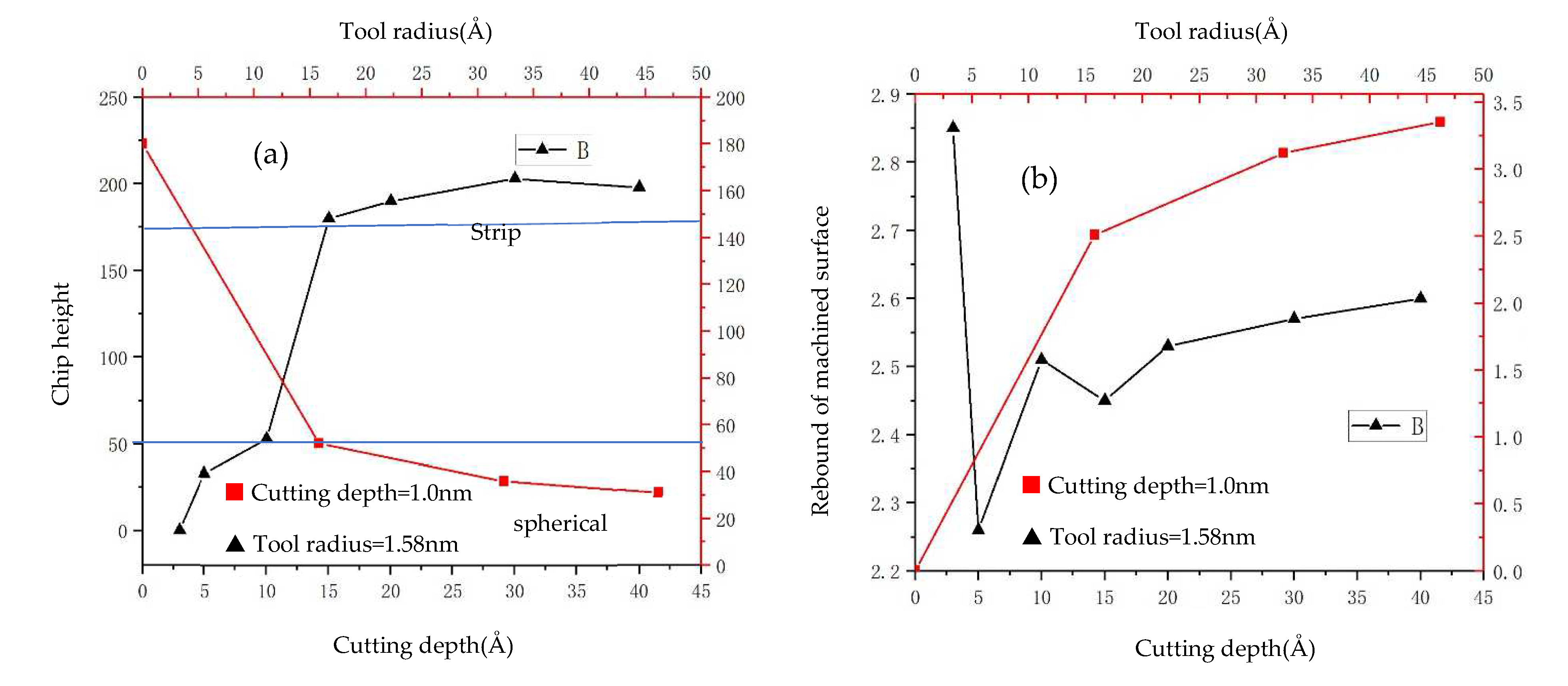
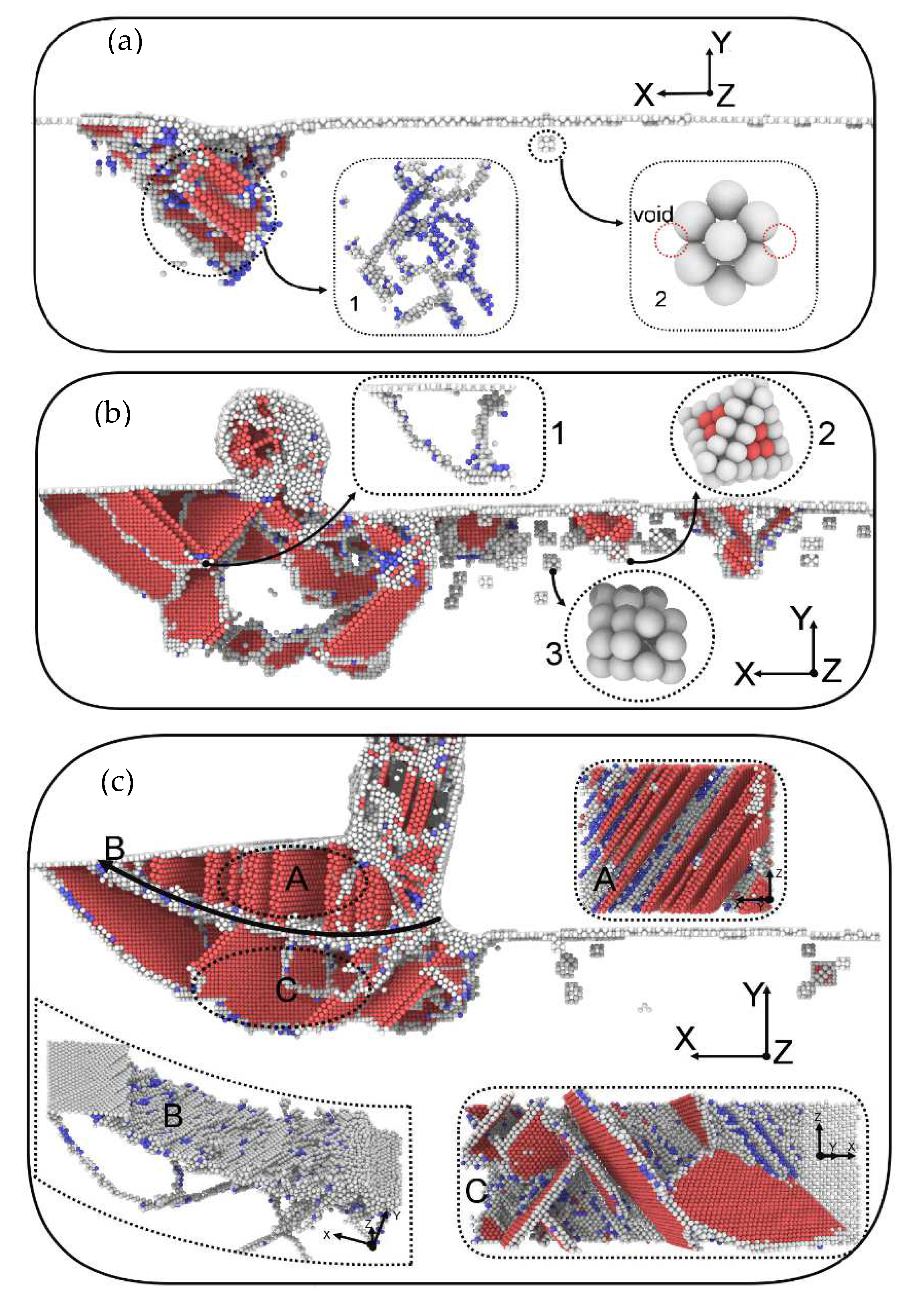
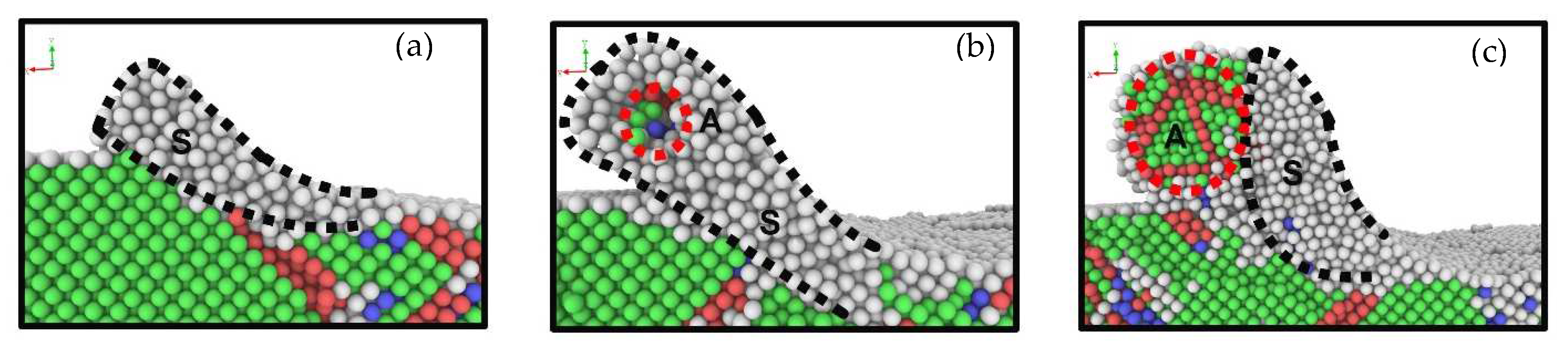
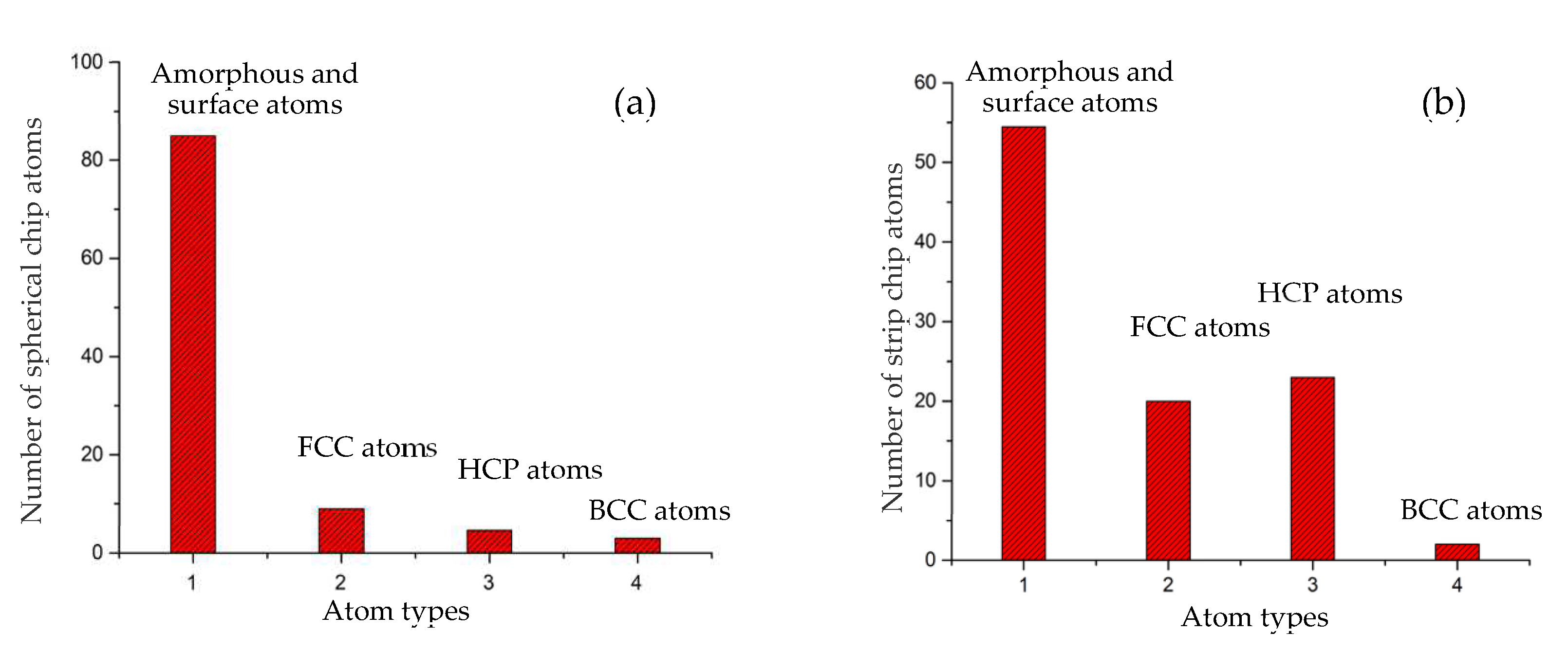
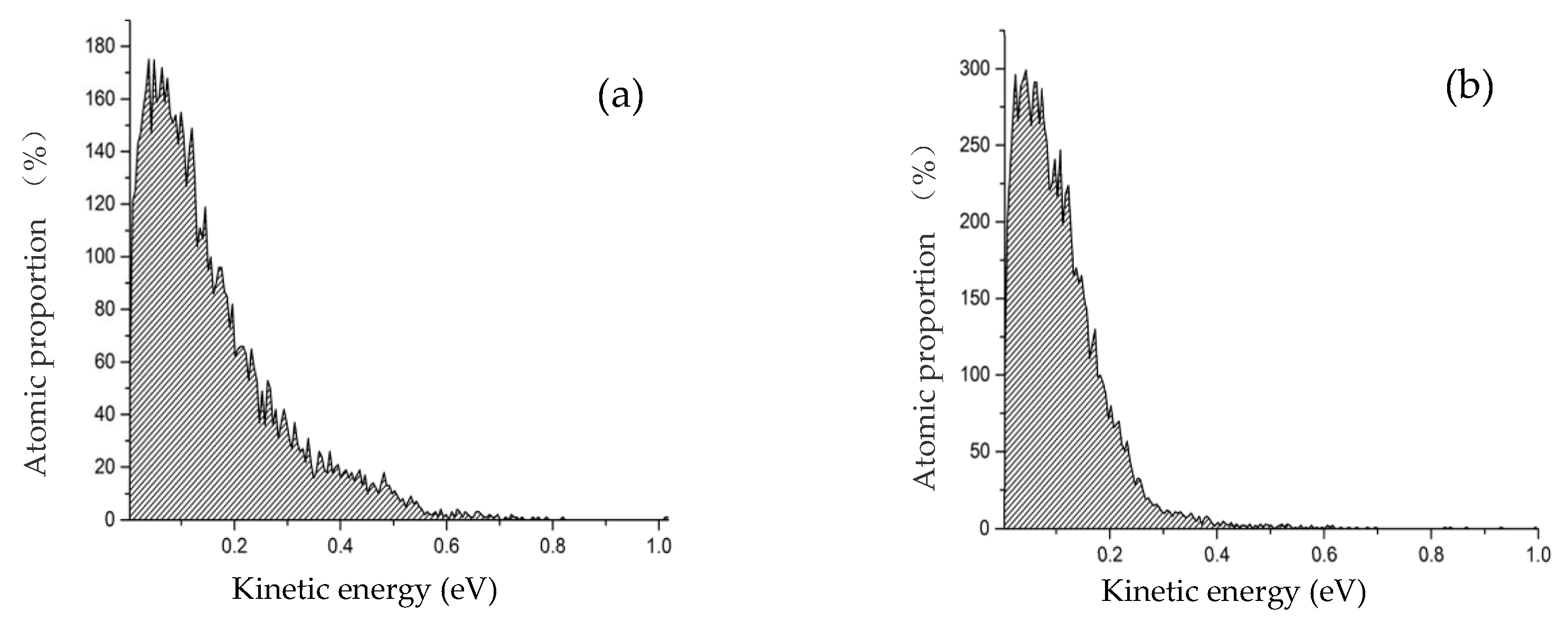
3.3. Chips at Different Machining States

As shown in Figure 15a, the arrangement of the atomic crystal structure of the spherical chip was disordered, owing to the crimping and continuous pushing of the cutter. The atomic composition of the chip was statistically analyzed, as depicted in Figure 16a. The results show that the ratio of surface and amorphous atoms in the spherical chip was high (almost 90%); therefore, the crystal structure in the chip was nearly destroyed.
As shown in Figure 15b, the arrangement of strip chip atoms was relatively neat. The arrangement direction of the HCP twin boundary was 45° with the Y and Z-axis, and the number of perfect FCC atoms and HCP atoms in the strip chip accounted for a considerable proportion. Additionally, the number of HCP atoms was greater than that of perfect FCC atoms, as shown in Figure 16b. This indicates that the crystal structure of the atoms in the strip chip were destroyed to a low degree, and more crystal atoms existed in the HCP structure.
The kinetic energy of the chip reflects the active degree of the chip atoms. As shown in Figure 17a, the atomic kinetic energy of the spherical chips was predominantly distributed in the range of 0–0.6 eV. The atomic kinetic energy of strip chips was primarily distributed in the range of 0–0.4 eV, as shown in Figure 17b. It was found that the number of atoms with high kinetic energy in the spherical chip was greater than that in the strip chip, and the maximum kinetic energy value of the atoms was, similarly, larger than that of the strip chip. This is largely because the spherical chip was always experiencing the pushing and friction action between the tool fillet and the rake face during machining, which caused the atomic energy in the chip to increase. Several perfect atomic bonds were broken during the curling and rolling process of the chip; thus, the chemical energy of the atomic bonds was converted into kinetic energy.

4. Conclusions

Three different machining states of nanoground single-crystal nickel were analyzed. It was found that the atoms in front of the tool were extruded inward during plowing, whereas the atoms in the back of the tool were affected by forward stretching and upward elastic recovery. The defects in front of the tool were characterized by large quantities and small volumes, dislocation tangles were formed, and the degree of subsurface damage was low. Although the machining depth was the smallest, the normal force was the largest.
When spherical chips were formed during the friction process, the removal of atoms by the tool primarily caused crowding damage, resulting in the formation of defects and complex structures in the workpiece. It was further found that the displacement vector of the spherical chip atoms diffused radially along the machining direction, the normal force was less than the plowing force, and the typical cylindrical defects were produced.
When strip chips were produced, the chip atoms were entirely removed and the displacement vectors were approximately the same. Although the machining depth was the largest, the normal machining was the smallest, and a dislocation tangle was formed in the early stages of machining. However, owing to the formation of slip channels, the machining efficiency was high, the tool wear was small, and subsurface damage was small.
In comparison, the arrangement of the spherical chip atoms was disordered, the proportion of amorphous atoms was high, and the overall atomic energy was large. However, the arrangement of strip chip atoms was regular, major forms of existence were predominantly formed by HCP twin boundaries and FCC crystals, and the overall atomic energy was small. The machined surface rebound was the largest during plowing, but it was the smallest when the spherical chip was produced. The rebound can therefore be ignored relative to the machining depth. The atomic kinetic energies of the spherical chip and strip chip showed different quantitative differences, and atomic stacking and disorder were formed. FCC and HCP atoms dominated the strip chips. The atomic kinetic energies of the two chips showed significant quantitative differences. The number of high-kinetic-energy atoms in the spherical chip was greater than that in the strip chip, and the maximum kinetic energy of the atom was also greater than that of the strip chip. The results show that the tool caused great damage to the matrix, forming spherical chips, fast chip accumulation, and significant damage to the complete crystal structure.

Author Contributions

Writing—original draft preparation, investigation, data curation, X.W. (Xingchun Wei) and Z.Z.; investigation, writing—review and editing, conceptualization, validation, X.W. (Xiaowen Wang) and T.S.; methodology, visualization, W.C. (Wenbang Chen) and B.P.; data processing, W.C. (Weihua Chen) and D.Q. All authors have read and agreed to the published version of the manuscript.

Funding

The project was supported by the National Natural Science Foundation of China (Grant No. 51966009) and the Natural Science Foundation of Gansu Province (20JR5RA462, 20JR5RA442).

Institutional Review Board Statement

Not applicable.

Informed Consent Statement

Informed consent was obtained from all subjects involved in the study.

Data Availability Statement

Data are contained within the article.

Conflicts of Interest

The authors declare no conflict of interest.

References

  1. Xiao, G.B.; He, Y.; Geng, Y.Q.; Yan, Y.D.; Ren, M.J. Molecular dynamics and experimental study on comparison between static and dynamic ploughing lithography of single crystal copper. Appl. Surf. Sci. 2019, 463, 96–104. [Google Scholar] [CrossRef]
  2. Xu, F.F.; Fang, F.Z.; Zhang, X.D. Effects of recovery and side flow on surface generation in nano-cutting of single crystal silicon. Comput. Mater. Sci. 2018, 143, 133–142. [Google Scholar] [CrossRef]
  3. Khoei, A.; Eshlaghi, G.T.; Shahoveisi, S. Atomistic simulation of creep deformation mechanisms in nickel-based single crystal superalloys. Mater. Sci. Eng. A 2021, 809, 140977. [Google Scholar] [CrossRef]
  4. Hao, Z.; Lou, Z.; Fan, Y. Study on staged work hardening mechanism of nickel-based single crystal alloy during atomic and close-to-atomic scale cutting. Precis. Eng. 2021, 68, 35–56. [Google Scholar] [CrossRef]
  5. Ren, J.; Hao, M.; Lv, M.; Wang, S.; Zhu, B. Molecular dynamics research on ultra-high-speed grinding mechanism of monocrystalline nickel. Appl. Surf. Sci. 2018, 455, 629–634. [Google Scholar] [CrossRef]
  6. Tu, H.; Zhang, G.F. Pile-up of dislocation while existing inhomogeneity. Acta Phys. Sin. 1988. [Google Scholar]
  7. Yan, Y.D.; He, Y.; Xiao, G.B.; Geng, Y.Q.; Ren, M.J. Effects of diamond tip orientation on the dynamic ploughing lithography of single crystal copper. Precis. Eng. 2019, 57, 127–136. [Google Scholar] [CrossRef]
  8. Zhu, Z.; Jiao, S.; Wang, H.; Wang, L.; Zheng, M.; Zhu, S.; Cheng, J.; Yang, J. Study on nanoscale friction and wear mechanism of nickel-based single crystal superalloy by molecular dynamics simulations. Tribol. Int. 2022, 165, 107322. [Google Scholar] [CrossRef]
  9. Abdulkadir, L.N.; Abou-El-Hossein, K.; Jumare, A.I.; Liman, M.M.; Olaniyan, T.A.; Odedeyi, P.B. Review of molecular dynamics/experimental study of diamond-silicon behavior in nanoscale machining. Int. J. Adv. Manuf. Technol. 2018, 98, 317–371. [Google Scholar] [CrossRef]
  10. Zheng, M.; Qu, D.; Wei, X.; Zhang, Z.; Zhu, Z.; Wang, L.; Chen, W. Molecular dynamics study on the nanoscale repeated friction and wear mechanisms of TiC/Ni composites. Appl. Phys. A 2022, 128, 1–18. [Google Scholar] [CrossRef]
  11. Dai, H.F.; Chen, G.Y.; Li, S.B.; Fang, Q.H.; Hu, B. Influence of laser nanostructured diamond tools on the cutting behavior of silicon by molecular dynamics simulation. RSC. Adv. 2017, 7, 15596–15612. [Google Scholar] [CrossRef] [Green Version]
  12. Zhang, L.; Zhao, H.W.; Dai, L.; Yang, Y.H.; Du, X.C.; Tang, P.Y.; Zhang, L. Molecular dynamics simulation of deformation accumulation in repeated nanometric cutting on single-crystal copper. RSC. Adv. 2015, 5, 12678–12685. [Google Scholar] [CrossRef]
  13. Lin, Y.C.; Shiu, Y.C. Effect of crystallographic orientation on single crystal copper nanogrooving behaviors by MD method. Int. J. Adv. Manuf. Technol. 2017, 89, 3207–3215. [Google Scholar] [CrossRef]
  14. Ren, J.; Hao, M.R.; Liang, G.X.; Wang, S.Y.; Lv, M. Study of subsurface damage of monocrystalline nickel in nanometric grinding with spherical abrasive grain. Phys. B Condens. Matter. 2019, 560, 60–66. [Google Scholar] [CrossRef]
  15. Cao, H.; Rui, Z.Y.; Chen, W.K.; Feng, R.C.; Yan, C.F. Deformation mechanisms in nanotwinned γ-TiAl by molecular dynamics simulation. Mol. Simul. 2018, 44, 1489–1500. [Google Scholar] [CrossRef]
  16. Li, J.; Fang, Q.H.; Liu, Y.W.; Zhang, L.C. Scratching of copper with rough surfaces conducted by diamond tip simulated using molecular dynamics. Int. J. Adv. Manuf. Technol. 2015, 77, 1057–1070. [Google Scholar] [CrossRef]
  17. Karkalos, N.E.; Markopoulos, A.P. Determination of the Efficiency of Hot Nano-Grinding of Mono-Crystalline Fcc Metals Using Molecular Dynamics Method. Micromachines 2022, 13, 415. [Google Scholar] [CrossRef]
  18. Huang, Y.H.; Zong, W.J. Molecular dynamic simulation for nanometric cutting of single-crystal face-centered cubic metals. Nanoscale Res. Lett. 2014, 9, 1–9. [Google Scholar] [CrossRef] [Green Version]
  19. Fang, Q.H.; Wang, Q.; Li, J.; Zeng, X.; Liu, Y.W. Mechanisms of subsurface damage and material removal during high speed grinding processes in Ni/Cu multilayers using a molecular dynamics study. RSC. Adv. 2017, 7, 42047–42055. [Google Scholar] [CrossRef] [Green Version]
  20. Eder, S.J.; Grützmacher, P.G.; Rodríguez Ripoll, M.; Dini, D.; Gachot, C. Effect of temperature on the deformation behavior of copper nickel alloys under sliding. Materials 2020, 14, 60. [Google Scholar] [CrossRef]
  21. Hao, Z.P.; Cui, R.R.; Fan, Y.H.; Lin, J.Q. Diffusion mechanism of tools and simulation in nanoscale cutting the Ni–Fe–Cr series of Nickel-based superalloy. Int. J. Mech. Sci. 2019, 150, 625–636. [Google Scholar] [CrossRef]
  22. Wang, Q.L.; Bai, Q.S.; Chen, J.X.; Sun, Y.Z.; Guo, Y.B.; Liang, Y.C. Subsurface defects structural evolution in nano-cutting of single crystal copper. Appl. Surf. Sci. 2015, 344, 38–46. [Google Scholar] [CrossRef]
  23. Wang, Y.; Tang, S.; Guo, J. Molecular dynamics study on deformation behaviour of monocrystalline GaN during nano abrasive machining. Appl. Surf. Sci. 2020, 510, 145492. [Google Scholar] [CrossRef]
  24. Xu, Y.X.; Wang, M.C.; Zhu, F.L.; Liu, X.J.; Chen, Q.; Hu, J.X.; Lu, Z.L.; Zeng, P.J.; Liu, Y.H. A molecular dynamic study of nano-grinding of a monocrystalline copper-silicon substrate. Appl. Surf. Sci. 2019, 493, 933–947. [Google Scholar] [CrossRef]
  25. Plimpton, S. Fast parallel algorithms for short-range molecular dynamics. J. Comput. Phys. 1995, 117, 1–19. [Google Scholar] [CrossRef] [Green Version]
  26. Thompson, A.P.; Aktulga, H.M.; Berger, R.; Bolintineanu, D.S.; Brown, W.M.; Crozier, P.S.; in’t Veld, P.J.; Kohlmeyer, A.; Moore, S.G.; Nguyen, T.D.; et al. LAMMPS—A flexible simulation tool for particle-based materials modeling at the atomic, meso, and continuum scales. Comput. Phys. Commun. 2022, 271, 108171. [Google Scholar] [CrossRef]
  27. Zhu, Z.; Peng, B.; Feng, R.; Wang, L.; Jiao, S.; Dong, Y. Molecular dynamics simulation of chip formation mechanism in single-crystal nickel nanomachining. Sci. China Technol. Sci. 2019, 62, 1916–1929. [Google Scholar] [CrossRef]
  28. Nosé, S. A unified formulation of the constant temperature molecular dynamics methods. J. Chem. Phys. 1984, 81, 511–519. [Google Scholar] [CrossRef] [Green Version]
  29. Rapaport, D.C.; Rapaport, D.C.R. The Art of Molecular Dynamics Simulation; Cambridge University Press: Cambridge, UK, 2004. [Google Scholar]
  30. Eder, S.J.; Cihak-Bayr, U.; Bianchi, D.; Feldbauer, G.; Betz, G. Thermostat influence on the structural development and material removal during abrasion of nanocrystalline ferrite. ACS Appl. Mater. Interfaces 2017, 9, 13713–13725. [Google Scholar] [CrossRef] [Green Version]
  31. Hao, Z.; Han, X.; Fan, Y.; Lou, Z. Microscopic Study on the Mechanism of Tool Bond Wear in Cutting Ni–Fe-Cr-Co–Cu Series Nickel-Base Superalloy. Int. J. Precis. Eng. Manuf. 2021, 22, 621–634. [Google Scholar] [CrossRef]
  32. Goel, S.; Luo, X.; Reuben, R.L. Wear mechanism of diamond tools against single crystal silicon in single point diamond turning process. Tribol. Int. 2013, 57, 272–281. [Google Scholar] [CrossRef]
  33. Guo, Y.; Liang, Y.; Chen, M.; Bai, Q.; Lu, L. Molecular dynamics simulations of thermal effects in nanometric cutting process. Sci. China Technol. Sci. 2010, 53, 870–874. [Google Scholar] [CrossRef]
  34. Hao Zhao, P.; Lou Zai, Z.; Fan Yi, H. Study on the evolution mechanism of subsurface defects in nickel-based single crystal alloy during atomic and close-to-atomic scale cutting. J. Manuf. Process 2021, 68, 14–33. [Google Scholar] [CrossRef]
  35. Daw, M.S.; Baskes, M.I. Embedded-atom method: Derivation and application to impurities, surfaces, and other defects in metals. Phys. Rev. B 1984, 29, 6443–6453. [Google Scholar] [CrossRef] [Green Version]
  36. Stowers, I.F.; Komanduri, R.; Baird, E.D. Review of precision surface generating processes and their potential application to the fabrication of large optical components. In Proceedings of the Advances in Fabrication and Metrology for Optics and Large Optics, San Diego, CA, USA, 29 January 1989; pp. 62–73. [Google Scholar]
  37. Nelson, J.; Daw, M.; Sowa, E.C. Embedded atom calculations of the Cu (001),(111), and (110) surface phonon spectra. Superlattices Microstruct. 1990, 7, 259–267. [Google Scholar] [CrossRef]
  38. Liu, H.; Wang, X.M.; Liang, H.; Zhao, Z.N.; Li, L.; Yue, Z.F.; Deng, C.H. The effect of void defect on the evolution mechanisms of dislocations and mechanical properties in nickel-based superalloys by molecular dynamics simulation of real γ/γ′ structures. Int. J. Solids Struct. 2020, 191, 464–472. [Google Scholar] [CrossRef]
  39. Tersoff, J. Modeling solid-state chemistry: Interatomic potentials for multicomponent systems. Phys. Rev. B 1989, 39, 5566. [Google Scholar] [CrossRef]
  40. Maekawa, K.; Itoh, A. Friction and tool wear in nano-scale machining—A molecular dynamics approach. Wear 1995, 188, 115–122. [Google Scholar] [CrossRef]
  41. Lin, Z.C.; Huang, J.C.; Jeng, Y.R. 3D nano-scale cutting model for nickel material. J. Mater. Process. Technol. 2007, 192, 27–36. [Google Scholar] [CrossRef]
  42. Ikawa, N.; Donaldson, R.R.; Komanduri, R.; König, W.; McKeown, P.A.; Moriwaki, T.; Stowers, I.F. Ultraprecision metal cutting—the past, the present and the future. CIRP Ann. 1991, 40, 587–594. [Google Scholar] [CrossRef]
  43. Stukowski, A. Visualization and analysis of atomistic simulation data with OVITO–the Open Visualization Tool. Model. Simul. Mater. Sci. Eng. 2009, 18, 015012. Available online: http://iopscience.iop.org/0965-0393/18/1/015012 (accessed on 15 March 2022). [CrossRef]
  44. Honeycutt, J.D.; Andersen, H.C. Molecular dynamics study of melting and freezing of small Lennard-Jones clusters. J. Phys. Chem. 1987, 91, 4950–4963. [Google Scholar] [CrossRef]
  45. Zhu, Z.X.; Gong, Y.D.; Zhou, Y.G.; Gao, Q. Molecular dynamics simulation of single crystal Nickel nanometric machining. Sci. China Technol. Sci. 2016, 59, 867–875. [Google Scholar] [CrossRef]
  46. Shu, X.Y.; Lu, Y.; Xin, T.J.; Li, Z.P.; Chen, Y.H.; Zhou, H.; Mao, S.C.; Liao, X.Z. In-situ investigation of dislocation tangle–untangle processes in small-sized body-centered cubic Nb single crystals. Mater. Lett. 2017, 198, 16–18. [Google Scholar] [CrossRef]
  47. Stukowski, A.; Bulatov, V.V.; Arsenlis, A. Automated identification and indexing of dislocations in crystal interfaces. Model. Simul. Mater. Sci. Eng. 2012, 20, 085007. Available online: http://stacks.iop.org/0965-0393/20/i=8/a=085007 (accessed on 15 March 2022). [CrossRef]
  48. Zhu, J.Q.; Liu, X.; Yang, Q.S. Dislocation-blocking mechanism for the strengthening and toughening of laminated graphene/Al composites. Comput. Mater. Sci. 2019, 160, 72–81. [Google Scholar] [CrossRef]
Figure 1. The nanomachining model of single-crystal nickel.
Coatings 12 00647 g001
Figure 2. Atomic displacement vector of workpiece at different chip states. Here, Δb represents the elastic recovery distance, and h is the height of the strip chip (nm). The machining depths of (a,b) are 0.3 and 0.5 nm respectively, and the tool radius is 1.58 nm, (c) the machining depth is 1nm and the tool radius is 4.62 and 0 nm. The red arrow indicates the displacement vector.
Coatings 12 00647 g002
Figure 3. Atomic displacement scatter plot for different chip states. (a) Both sides of the tip; (b) The spherical chips; (c) The strip chips.
Coatings 12 00647 g003
Figure 4. Line plots of chip height and rebound. (a) Variation in chip height when the cutting depth was 1 nm and tool radius was 1.58 nm; and (b) variation in rebounding on the machined surface when the chip depth was 1 nm and the tool fillet was 1.58 nm.
Coatings 12 00647 g004
Figure 5. Change in tangential forces, normal forces, and friction coefficients at different chip states. (a) Change in tangential forces at different chip states; (b) change in normal forces at different chip states; and (c) change in ratio of tangential force to normal force at different chip states.
Coatings 12 00647 g005
Figure 6. Internal defects of the workpiece at different chip states. (a) Plowing, (b) spherical chip, and (c) strip chip. Red represents HCP atoms, white represents surface and amorphous atoms, and blue represents BCC atoms.
Coatings 12 00647 g006
Figure 7. Formation process of a dislocation tangle in the plow machining state. The machining distances in (ad) are 12, 13, 14, and 20 nm, respectively. Here, indigo, pink, gray, blue, purple, and yellow represent Shockley, perfect, stair-rod, Frank, Hirth, and other dislocations, respectively.
Coatings 12 00647 g007
Figure 8. Number, length, and density change in dislocations during plowing. (a) Change in number of dislocations; (b) changve in dislocation length; and (c) change in dislocation density.
Coatings 12 00647 g008
Figure 9. The crystal structure change diagram of the spherical chip formation process. (ac) is a continuous process of spherical chip formation, green, red, blue and white are FCC, HCP, BCC and other structural atoms respectively.
Coatings 12 00647 g009
Figure 10. Schematic diagram of spherical chip movement. A is the rolling direction of spherical chips; S is the flow direction of chip atoms; and V is the direction of tool movement.
Coatings 12 00647 g010
Figure 11. Columnar defect and standard FCC structure with the specific parameter. (a) is a columnar defect, (b,c) show the atomic arrangement of the defect and the perfect FCC, respectively. The red atom is the atom leaving the lattice point.
Coatings 12 00647 g011
Figure 12. Dislocation jog reaction process. (ac) is a continuous dislocation jog reaction formed by columnar defects.
Coatings 12 00647 g012
Figure 13. Dislocation block.
Coatings 12 00647 g013
Figure 14. Slip channel formation process. (a) Defect displacement diagram; and (b) schematic diagram. (a1c1) is the schematic diagram diagram corresponding to (ac).
Coatings 12 00647 g014
Figure 15. Crystal structure of the different chips. (a) Crystal structure of the spherical chip; and (b) crystal structure of strip chip. Green, red, blue and white are FCC, HCP, BCC and other structural atoms respectively.
Coatings 12 00647 g015
Figure 16. Atomic proportions of different chip forms. (a) Proportion of different atoms in the spherical chip; and (b) proportion of different atoms in strip chip.
Coatings 12 00647 g016
Figure 17. Instantaneous atomic kinetic energy distribution of different chip forms. (a) Kinetic energy distribution of spherical chip; and (b) kinetic energy distribution of strip chip.
Coatings 12 00647 g017
Table 1. MD Simulation parameters of nanomachining.
Workpiece MaterialSingle-Crystal Nickel
Tool materialDiamond
Rake15°
Radius (nm)0, 1.58, 3.24, 4.62
Clearance angle
Machining depth (nm)0.3, 0.5, 1, 1.5, 2, 3, 4
Machining speed200 m/s
Machining direction[100] on (100) surface
Steps1 fs
Publisher’s Note: MDPI stays neutral with regard to jurisdictional claims in published maps and institutional affiliations.

