1. Introduction
Spectral analysis has been applied in scientific research and industrial production because of its sensitivity, rapidity, and accuracy [
1,
2,
3]. In addition, since the spectrometers need to become more portable and stable to be capable of on-site applications, miniaturization is a very important development trend [
4,
5].
In order to reduce the volume of spectrometers, many scholars have made great efforts in various aspects [
6], such as the innovation of diffractive elements. A concave grating is used to replace a plane grating to reduce the number of reflective elements [
7]. The metasurface is also proved to be a diffractive optical element, achieving a resolution of 1.2 nm and an ultra-small volume of 7 mm
3 [
8,
9]. In addition, the progress of photodetectors has also promoted the development of higher performance micro spectrometers. Many new materials, such as graphene and metamaterials, provide more possibilities for highly sensitive photodetectors [
10,
11]. Long-wave perfect absorbers based on plasma resonance will drive the development of infrared photodetectors in the future [
12]. Ref. [
13] introduces the development direction and present situation of miniature spectrometers achieved in recent years.
As a substitute for a free-propagating optical system, researchers used mirrors or a high refractive index medium to fold the dimensions of the sagittal plane, which further reduced the size of the overall optical system. This foldable optical system could satisfy the demand for the miniaturization of spectrometers, interferometers and other optical systems of 1D spectral responses [
14]. The planar waveguide spectrometer based on the folded light path be easily integrated into handheld devices or space-efficient devices to provide spectrum detection services.
Foster-Miller developed wedge plane waveguide spectrometers by using highly refractive index materials, such as ZnSe, where column grating is connected to a wedge waveguide by a matched refractive index optical adhesive. The overall volume and weight of spectrometers are significantly reduced [
15]. With the continuous development of micro-electro-mechanical system (MEMS) technology, the Insion company has developed a hollow planar waveguide spectrometer (HPWS) based on MEMS technology. The air is the medium, and two gilded mirrors are used as reflectors. The overall structure is processed using Lithographie, Galvanoformung and Abformung (LIGA) technology for fully automated production [
16,
17]. Seung-Hun Oh et al. proposed an integrated polymeric spectrometer fabricated by UV imprint lithography, which had a resolution of 5 nm for spectral band of 250 nm [
18].
Table 1 provides a comparison of the key features of several micro spectrometers from the recent literature. The excellent achievements of the waveguide spectrometers above allowed for a thorough analysis of the structure, resolution and volume of the spectrometers. As a performance parameter for spectrometers, energy or sensitivity is as important as resolution, and so is HPWS. However, for the HPWS, the absorption and scattering of the mirror will cause a great loss of energy. If the numerical aperture (NA) of the light source is constant, the thickness of the HPWS determines the number of reflections of the beam in the sagittal plane. Clearly, the thinner the thickness, the more reflections and the greater the loss. On the other hand, the increased thickness would lead to a larger volume. In order to reduce Fresnel reflections, C.J. Moran-Iglesias et al. proposed adding a collimator lens in front of the slits and using fiber arrays instead of one single fiber. However, no specific design theory has been proposed.
In our previous work, we argued that the spectrometer could be analyzed in two directions. According to Coddington’s equation, the throughput and resolution of arc vector plane and meridian plane were theoretically analyzed, so that higher spectral resolution could be achieved and a more concentrated energy could be obtained [
19,
20]. Resolution was a factor in the direction of dispersion, which was concerned with the tangential plane. Optical flux was the characterization of how much the detector collects the energy in the sagittal plane. In this paper, an HPWS based on a Czerny–Turner (C–T) structure is designed from two aspects: the tangential plane and the sagittal plane. Then, the design result is given and the influence of the height of the waveguide (the distance between two parallel mirrors) on the energy received by the detector is discussed.
2. Design in the Tangential Plane
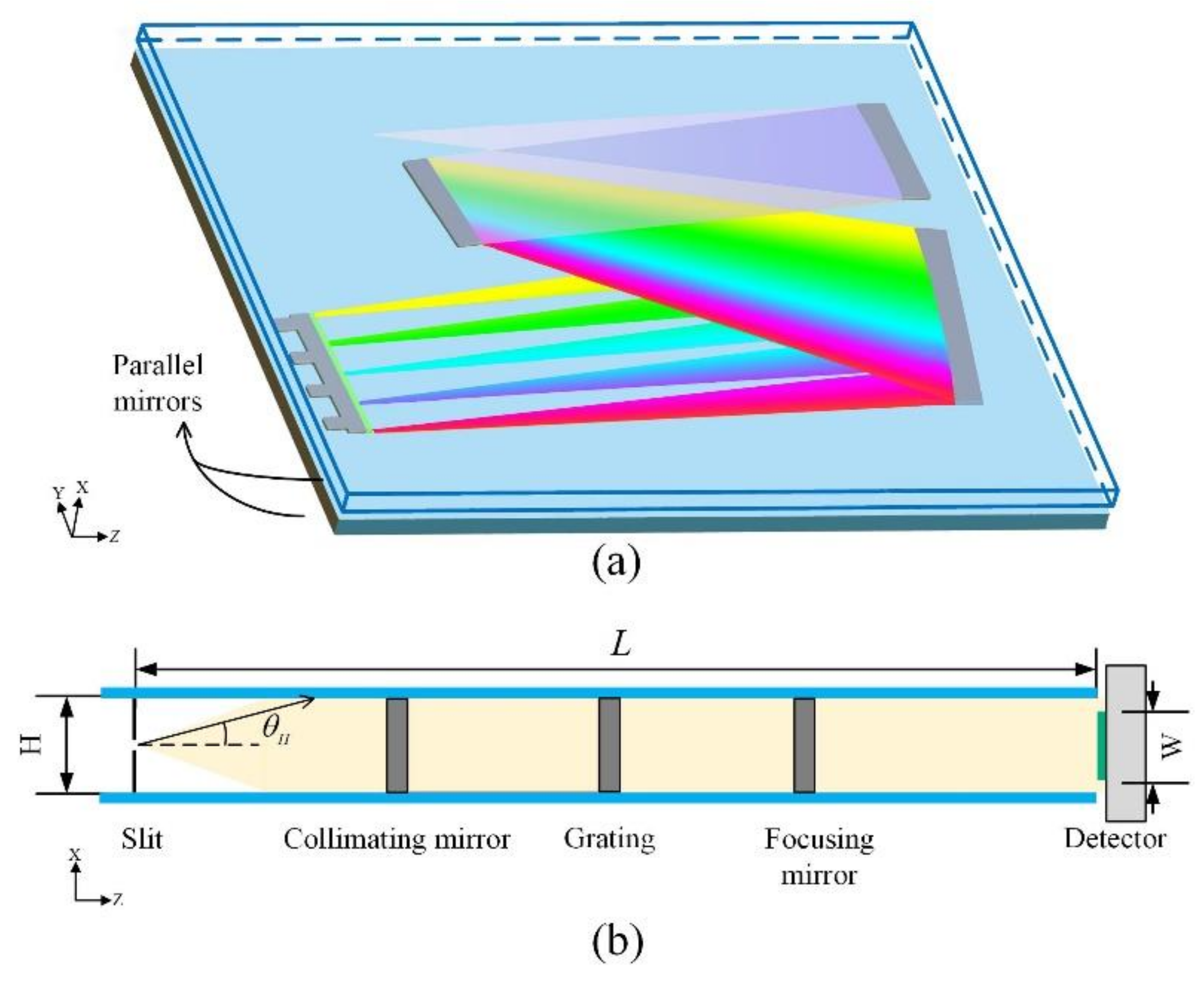
The optical components of a conventional C–T spectrometer include a grating, a collimating mirror, and a focusing mirror. The light beams travel through the collimating mirror and are diffracted by the grating after collimation. Then, the beams from various angles focus on the different points of the detector through the focusing mirror.
Unlike a conventional C–T spectrometer, the collimating mirror and focusing mirror of PWS are cylindrical mirrors instead of spherical mirrors. The light beam travels between the two parallel mirrors through the medium of air, as shown in
Figure 1. For the diffraction grating, the following formulation can be obtained:
where
i is the incident angle of the diffraction grating,
θ is the diffraction angle of the diffraction grating, and
δ is the angle between the incident beam and the diffraction beam. Then, the grating equation reads:
where
d is the grating constant, and
m is the diffraction order. In the central wavelength
λC, the incident angle
iC of the grating is derived by combining Equations (1) and (2):
The spectrometer ranges from 450 to 750 nm, the grating constant d in this example is set to 1.67 μm. Considering the compact structure, if the angle δC = 30°, then iC = 25.74° and θC = 4.26° can be obtained according to Equation (3).
In general, the focal length of the collimating mirror is related to the resolution. Considering the structure of the light path, the focal length of collimating mirror f1 is 40 mm, while the focal length of focusing mirror f2 is 45 mm.
The tilt angle of the collimating mirror
φ1 is set near the smallest angle to decrease the off-axis angle. The tilt angle of the focusing mirror
φ2 is calculated by the Shafer formulation to correct the coma; the angle
φ2 can be obtained according to Shafer [
21]:
where
R1 and
R2 are the radius of the collimating mirror and the focusing mirror respectively. The initial parameters in the tangential plane are calculated by using the aforementioned method.
3. Design in the Sagittal Plane
In the sagittal plane, the radius of collimating and focusing mirrors is infinity. Each light ray is assumed to carry the same amount of power in the light source, and the density of the light beam depends on the divergence angle.
L represents the projection of the optical path of HPWS onto the tangential plane. The number of reflections of a light ray emitted from the light source only depends on the height angle
θH (the angle between the light ray and the tangential plane) and the height
H (the distance between the two parallel mirrors) when
L is determined, as is shown in
Figure 1b. Therefore, considering the reflection of the spherical mirrors, the number of reflections in the system can be derived as:
where a is the number of spherical mirrors. The number of reflections
t is directly proportional to the tangent of the height angle
θH. The propagation efficiency of a single ray is:
where
τ is the reflectivity of the parallel mirrors. The propagation efficiency is calculated separately at different height angles. Then, the incident luminous flux is multiplied by the propagation efficiency
ηP and then by the diffraction efficiency
ηD of the grating at different wavelengths to obtain the output luminous flux Φ
out at this height angle:
The total output optical flux is the sum of the output optical flux at different height angles in the whole height angle range. The optical flux received by the detector can be described as:
where
W is the height of the detector. When the distance between the two parallel mirrors is greater than the height of the detector, the light beyond the detector is not collected.
In order to verify the results of calculations, a model of planar waveguide spectrometer was established. The design results and simulation model are given in
Section 4.
4. Simulation and Ray Tracing
In this section, a design example of an HPWS is presented. The optical design strategy of the HPWS is mentioned in
Section 2 and
Section 3. The fixed and optimized parameters are shown in
Table 2 and
Table 3, respectively. Since the optical path of the HPWS is not strictly ordered, the non-sequential mode of Zemax is selected. The initial optical path was input into the non-sequence mode, the angles were set as
φ1,
φ2, and the tilt angle of the detector
φ3 and the distance between the focusing mirror and the detector
LM2D were set as variables and optimized. The simulation model is shown in
Figure 2.
When the design of the optical path on the tangential plane is completed, the value of
L is determined. In this example, the NA of the light source is 0.12, the value of
L is 151.28 mm. A linear array detector is the most common detector type for miniature spectrometers. As a typical value for a linear array detector, the height of the detector is set to 0.2 mm. The pattern of the beam on the detector can be easily obtained. This pattern is shown in
Figure 3. The selected sampling wavelengths are 450, 600 and 750 nm, respectively. It is observed that the spectral resolution is better than 4nm in the spectral range.
The calculation procedure of the optical flux received by the detector is provided in
Section 3. The model is also established and simulated by Tracepro software (version 7.0.3). The total power of the light source is set to 1 W, the reflectivity of the two parallel mirrors and two spherical mirrors is set to 0.97 (similar to Au coating), and the surface property of the detector is set to complete absorption. The optical flux is obtained by tracing a large number of light rays.
5. Discussion
The simulated image from the detector is processed. The function curve of optical flux with respect to the height of the waveguide is drawn, as shown in
Figure 4. The calculation and simulation results of the optical flux incident onto the detector at different waveguide heights can be intuitively observed. This shows that the calculation results are in good agreement with the simulation results and proves that Equation (8) can be used to calculate the optical flux of the detector. Therefore, through Equation (8), it is convenient to quickly calculate the detector surface energy at different waveguide heights. In this example, for the detector, of which the pixel height is 0.2 mm, the optical flux received by the detector reaches a peak when the waveguide height is 0.2 mm, which is matched to the pixel height.
For a detector with a pixel height of 0.2 mm, the optical flux received by the detector reaches a peak when the waveguide height is close to the pixel height. For a conventional spectrometer, to eliminate the influence of astigmatism, it is necessary to add special optical elements or adopt special surface shapes in the optical path.
6. Conclusions
In this work, a hollow planar waveguide spectrometer (HPWS) was designed. The design process was independently carried out from the tangential and the sagittal planes. The parameters of the optical structure were derived in the tangential plane. Meanwhile, on the sagittal plane, a design theory and method was proposed to quantify the energy received by the detector and assist in its optimal design. Moreover, the relationship between the optical flux received by the detector and the height of the HPWS in the sagittal plane was discussed. The optical model was also established and simulated by raytracing software. The resolution of the HPWS was better than 4 nm, and the theoretical calculation of the optical flux received by the detector was almost consistent with the simulation results. Moreover, a detector with a pixel height of 0.2 mm is selected in the simulation. The results show that the highest energy was obtained when the thickness of the HPWS matched the height of the detector pixel. This work provides a reference for designing a hollow planar waveguide spectrometer. In the future, we will implement an HPWS with MEMS technologies. The main challenge is to make mirrors with a sufficient reflectivity and to achieve the parallelism of the two mirrors. Meanwhile, we hope to explore more design theories for other structural forms of waveguide spectrometers, such as a concave grating spectrometer.
Author Contributions
Conceptualization, G.X. and S.J.; software, L.Z. and Y.L.; validation, Z.F.; visualization, L.G. and W.S.; methodology and writing, Z.L. All authors have read and agreed to the published version of the manuscript.
Funding
This work is funded by the Science and Technology Planning Project of Guangdong Province (Grant No. 2018A01006).
Institutional Review Board Statement
Not applicable.
Informed Consent Statement
Not applicable.
Data Availability Statement
Not applicable.
Conflicts of Interest
The authors declare no conflict of interest.
References
- Sanchez, L.; Farber, C.; Lei, J.X.; Zhu-Salzman, K.; Kurouski, D. Noninvasive and Nondestructive Detection of Cowpea Bruchid within Cowpea Seeds with a Hand-Held Raman Spectrometer. Anal. Chem. 2019, 91, 1733–1737. [Google Scholar] [CrossRef] [PubMed]
- Correia, R.M.; Domingos, E.; Tosato, F.; Santos, N.A.D.; Leite, J.D.A.; da Silva, M.; Marcelo, M.C.A.; Ortiz, R.S.; Filgueiras, P.R.; Romão, W. Portable near infrared spectroscopy applied to abuse drugs and medicine analyses. Anal. Methods 2018, 10, 593–603. [Google Scholar] [CrossRef]
- Ferrari, M.; Quaresima, V. A brief review on the history of human functional near-infrared spectroscopy (fnirs) development and fields of application. Neuroimage 2012, 63, 921–935. [Google Scholar] [CrossRef] [PubMed]
- Malinen, J.; Rissanen, A.; Saari, H.; Karioja, P.; Karppinen, M.; Aalto, T.; Tukkiniemi, K. Advances in miniature spectrometer and sensor development. Proc. SPIE 2014, 9101, 83–97. [Google Scholar]
- Crocombe, R.A. Portable Spectroscopy. Appl. Spectrosc. 2018, 72, 1701–1751. [Google Scholar] [CrossRef] [PubMed]
- Goldman, D.S.; White, P.L.; Anheier, N.C.; Sriram, S. Planar waveguide spectrometer. Proc. SPIE 1990, 1338, 64–68. [Google Scholar]
- Mini-spectrometer C12666MA. Available online: http://www.hamamatsu.com.cn/product/16526.html (accessed on 30 March 2022).
- Faraji-Dana, M.S.; Arbabi, E.; Arbabi, A.; Kamali, S.M.; Kwon, H.; Faraon, A. Compact folded metasurface spectrometer. Nat. Commun. 2018, 9, 4196. [Google Scholar] [CrossRef] [PubMed]
- Zhu, A.Y.; Chen, W.-T.; Khorasaninejad, M.; Oh, J.; Zaidi, A.; Mishra, I.; Devlin, R.C.; Capasso, F. Ultra-compact visible chiral spectrometer with meta-lenses. APL Photonics 2017, 2, 036103. [Google Scholar] [CrossRef] [Green Version]
- Chen, H.; Chen, Z.; Yang, H.; Wen, L.; Yi, Z.; Zhou, Z.; Dai, B.; Zhang, J.; Wu, X.; Wu, P. Multi-mode surface plasmon resonance absorber based on dart-type single-layer graphene. RSC Adv. 2022, 12, 7821–7829. [Google Scholar] [CrossRef]
- Zheng, Z.; Zheng, Y.; Luo, Y.; Yi, Z.; Zhang, J.; Liu, Z.; Yang, W.; Yu, Y.; Wu, X.; Wu, P. Switchable terahertz device combining ultra-wideband absorption and ultra-wideband complete reflection. Phys. Chem. Chem. Phys. 2022, 24, 2527–2533. [Google Scholar] [CrossRef] [PubMed]
- Zhao, F.; Lin, J.; Lei, Z.; Yi, Z.; Qin, F.; Zhang, J.; Li liu, X.W.; Yang, W.; Wu, P. Realization of 18.97% theoretical efficiency of 0.9 µm Thick c-Si/ZnO Heterojunction Ultrathin-film Solar Cells via Surface Plasmon Resonance Enhancement. Phys. Chem. Chem. Phys. 2022, 24, 4871–4880. [Google Scholar] [CrossRef] [PubMed]
- Yang, Z.; Albrow-Owen, T.; Cai, W.; Hasan, T. Miniaturization of optical spectrometers. Science 2021, 371, 480–492. [Google Scholar] [CrossRef] [PubMed]
- Hakkel, K.D.; Petruzzella, M.; Ou, F.; van Klinken, A.; Pagliano, F.; Liu, T.; van Veldhoven, R.P.J.; Fiore, A. Integrated near-infrared spectral sensing. Nat. Commun. 2022, 13, 103. [Google Scholar] [CrossRef] [PubMed]
- Chadha, S.; Stevenson, C.; Curtiss, L.E. High-throughput infrared spectrometer for standoff chemical detection. Proc. SPIE 1999, 3533, 103–113. [Google Scholar]
- Krippner, P.; Kuehner, T.; Mohr, J.; Saile, V.; Mariella, R.P. Microspectrometer system for the near-infrared wavelength range based on liga technology. Proc. SPIE 2000, 3912, 141–149. [Google Scholar]
- Mazuray, L.; Moran-Iglesias, C.J.; Wartmann, R.; Last, A.; Mohr, J. Improved grating microspectrometer. Opt. Des. Eng. II 2005, 5962, 660–668. [Google Scholar]
- Oh, S.; Ahn, K.; Choi, H. Fabrication of integrated spectrometer module based on optical waveguide platform with planar nano diffraction grating using UV imprint lithography. Microelectron. Eng. 2019, 217, 111130. [Google Scholar] [CrossRef]
- Feng, Z.; Xia, G.; Lu, R.; Cai, X.; Hu, M. High performance ultrathin spectrometer optical design based on Coddington’s equations. Sensors 2021, 21, 323. [Google Scholar] [CrossRef] [PubMed]
- Guo, X.; Su, W.; Wang, G.; Hu, M.; Xing, J. Astigmatism-free Czerny–Turner compact spectrometer with cylindrical mirrors. Appl. Opt. 2017, 56, 9069–9073. [Google Scholar]
- Shafer, A.B.; Megill, L.R.; Droppleman, L. Optimization of the Czerny–Turner Spectrometer. J. Opt. Soc. Am. 1964, 54, 879–887. [Google Scholar] [CrossRef]
| Publisher’s Note: MDPI stays neutral with regard to jurisdictional claims in published maps and institutional affiliations. |
© 2022 by the authors. Licensee MDPI, Basel, Switzerland. This article is an open access article distributed under the terms and conditions of the Creative Commons Attribution (CC BY) license (https://creativecommons.org/licenses/by/4.0/).


