Article

Spin-Current Oscillations in Diluted Magnetic Semiconductor Multibarrier GaMnAs/GaAs: Role of Temperature and Bias Voltage

by
Najla S. Al-Shameri
and
Hassen Dakhlaoui
*
Basic and Applied Scientific Research Center (BASRC), Physics Department, College of Science of Dammam, Imam Abdulrahman Bin Faisal University, Dammam 31441, Saudi Arabia
*
Author to whom correspondence should be addressed.
Coatings 2022, 12(4), 504; https://doi.org/10.3390/coatings12040504
Submission received: 8 March 2022 / Revised: 31 March 2022 / Accepted: 6 April 2022 / Published: 8 April 2022
(This article belongs to the Special Issue Optical Thin Films: Preparation, Application and Development)

Abstract

:
This paper has studied the electronic properties of multi-diluted magnetic semiconductor (DMS) layers Ga(1 − x)MnxAs interposed between nonmagnetic GaAs layers. The asymmetry of confining potential on the transmission coefficient by tuning the temperature and the size of the (DMS) layers was discussed. The diluted magnetic layers Ga(1 − x)MnxAs behave as barriers for spin-up holes and quantum wells for spin-down holes. Furthermore, we have addressed the impact of an applied bias voltage and the temperature on the variation of the spin-polarization and spin current densities. Our findings reveal that the transmission coefficients present an oscillating behavior due to the resonant states and strongly depend on the temperature of the system and the number of magnetic layers. Furthermore, the obtained results demonstrated that the number of these states is multiplied by augmenting the magnetic layers. Moreover, we demonstrate that the asymmetric structure presents a completely different transmission of holes than the symmetric structure. Furthermore, the negative differential resistance (NDR) is demonstrated in the current density variations. Especially, this (NDR) was more intense for spin-up holes than spin-down holes. The findings in the present paper can be useful in manufacturing spin-filters by adjusting the values of the temperature and the external voltages.

1. Introduction

Recently, the study of the transport phenomenon in diluted magnetic semiconductors (DMS), especially the injection, transmission, and detection of spin-dependent carriers into devices based on III–V semiconductors has become one of the most important problems in the enhancement of the spintronics area, which represents a huge magnitude as a new field in quantum physics [1,2,3,4,5,6,7,8,9,10,11]. Spin-dependent transport has gained great interest because it permits the creation and manufacturing of important devices, such as the spin-field effect transistors, the spin-light emitting diodes, and quantum computers [12,13,14,15].
It is proven that the juxtaposition of the multibarrier system formed by nonmagnetic/magnetic semiconductors can serve in the injection and detection of spin-polarized carriers. Egues [16] was the first who theoretically studied spin-dependent tunneling across a single diluted magnetic semiconductor barrier. After that, there has been a growing benefit in enhancing the spin-polarized semiconductor devices and employing the spin-charged carriers in solid state devices to be used in quantum information storage and computing [12,13].
Among the various kind of (DMS) materials, Ga(1 − x)MnxAs are still the most preferred semiconductor used in different spintronics applications. In this semiconductor, Mn ions, which act as acceptors, substitute a fraction of Ga atoms leading to additional holes in the host material. The five electrons localized in the “3d’’ shell of Mn2+ ions produce localized magnetic moments. The interaction between the spin of these ions and those of the holes, also known as ‘p-d’ coupling, produces the ferromagnetism phenomenon in these materials [17,18]. The ferromagnetism in Ga(1 − x)MnxAs, which occurs above the Curie temperature (Tc), depends on the Mn concentration (xMn). For xMn = 0.05, Tc is equal to 110 K. Despite this small value of Tc, GaMnAs remains a beneficial material since it presents supplementary advantages compared to other materials. For instance, this semiconductor provides easier integration for quantum structures than other DMS materials.
The transmission of holes and their polarization across multi-magnetic barriers has attracted much attention in studying the spin-polarized transport phenomena, especially in quantum structures based on Ga(1 − x)MnxAs sandwiched between GaAs or AlAs semiconductors. For instance, Saffarzadeh et al. [19] studied the tunneling magnetoresistance (TMR) in a GaMnAs/GaAs/GaMnAs heterostructure, considering a spin-splitting effect. Their results show that the (TMR) decreases strongly with augmenting the barrier thickness and the externally applied voltage. Tao et al. [20] studied the transmission of holes across a magnetic tunnel junction based on a quantum-mechanical approach. They proved that the conductance decreases with temperature. Ju et al. [21] investigated magnetoresistance in a GaMnAs/AlAs/GaMnAs single barrier, reporting that the (TMR) could be enhanced by the presence of the pinholes in the thin barrier separating the magnetic layers.
Motivated by all the previous works, in the present work, we address the spin-dependent transmission of holes across heterostructures containing multi (DMS) semiconductors. The main goal of this work is to show how multibarrier systems based on (DMS) semiconductors could present different transmission and spin-polarizations, which are strongly required in the realization of spin-filter devices.
We have organized the paper as follows: In Section 2, we introduce the Hamiltonian describing the system’s total energy, and we display the expression of the transmission coefficient. Then, in Section 3, the numerical results are outlined and discussed. Finally, the main findings are summarized in the conclusion.

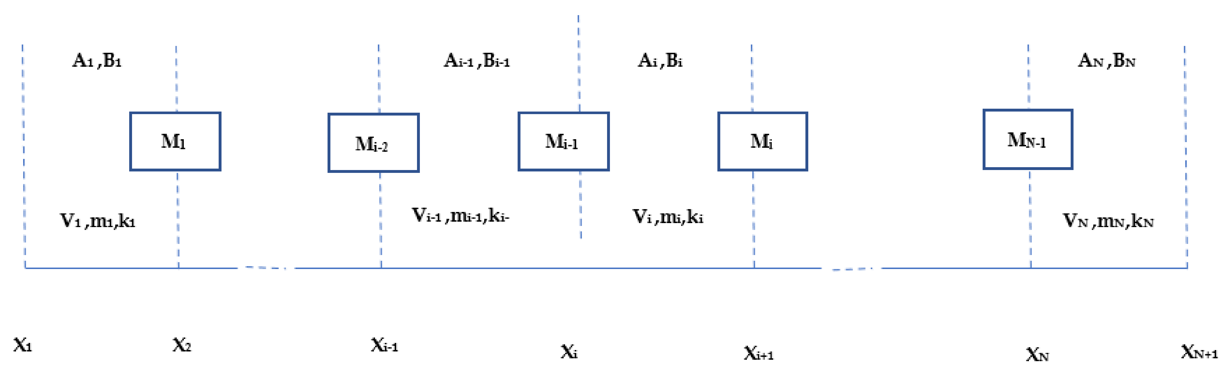
2. Theoretical Method

The transfer matrix method (TMM) has been largely employed to study the transport phenomena in quantum structures, such as quantum wells and wires, and it represents an adequate computing technique to determine the resonant states for various quantum confinement potentials.
In the present paper, we aim to study the transmission coefficient T(E), the spin polarization P(E), and the current density for a great number of magnetic (GaMnAs) and nonmagnetic (GaAs) layers using the (TMM) approach.
An arbitrary potential profile describing the confinement potential of N layers can be divided into several piecewise segments as shown in Figure 1, where each segment has an effective mass and confining potential.
Additionally, depending on the potential profile we can regard the potential in each segment as constant or linear. Additionally, by transferring matrices based on boundary conditions, we can link the coefficients of the wavefunction in each segment to those in the adjacent segment. Finally, we can solve scattering and eigenfunctions problems by using the transfer matrix method. The one-dimensional Schrödinger equation along the growth axis (ox) can be written in the following form:
2 2 m i * d 2 ψ i ( x ) d x 2 + V i ( x ) ψ i ( x ) = E i ψ i ( x )
where ψ i , E i represent, the wave function and the corresponding energy level, respectively. is the reduced Planck’s constant, m i * is the effective mass and V i is the spin-dependent potential of the segment i. The solution of the time-independent Schrödinger equation in each segment can be written as:
ψ i ( x ) = A i e j k i x + B i e j k i x ( x i x x i + 1 )
where A i , B i are the transmission and reflection coefficients, respectively, k i is the wave vector.
k i = 2 m i * ( E V i )
k i has real values for E > V i and imaginary for E < V i . Using the continuity of the wavefunction and its first derivative at each interface between two consecutive layers makes it possible to connect the wave function coefficients corresponding to segment i to those of the segment i + 1 by a matrix equation.
ψ i ( x i + 1 ) = ψ i + 1 ( x i + 1 )
1 m i * d ψ i ( x i + 1 ) d x = 1 m i + 1 * d ψ i + 1 ( x i + 1 ) d x
A i B i = M i A i + 1 B i + 1
where Mi represents the transfer matrix.
M i = 1 2 1 + k i + 1 m i k i m i + 1 exp [ j ( k i + 1 k i ) x i + 1 ] 1 k i + 1 m i k i m i + 1 exp [ j ( k i + 1 + k i ) x i + 1 ] 1 k i + 1 m i k i m i + 1 exp [ j ( k i + 1 + k i ) x i + 1 ] 1 + k i + 1 m i k i m i + 1 exp [ j ( k i + 1 k i ) x i + 1 ]
Finally, the amplitudes of the initial and last layers are connected as follows:
A 1 B 1 = M 1 M 2 M N 1 A N B N
A i B i = T A N B N
where T = i = 1 N 1 M i .
For the tunneling problem, we can calculate the transmission coefficient, which is the ratio of reflectivity and transmission as follows:
T r a n ( E ) = m 1 k N m N k 1 1 T 11 2
The wavevector in barrier regions contains the spin-dependent potential V σ . This potential depends on the temperature of the system. All the values of V σ used here are taken from reference [22,23]. In fact, this potential makes the magnetic layer act as a quantum well for spin-up holes and as a barrier for spin-down holes.
Once the transmission coefficient is evaluated, we calculated the spin polarization, defined as follows [24,25,26]:
P ( E ) = T u p ( E ) T d o w n ( E ) T u p ( E ) + T d o w n ( E )
As stated by the Tsu–Esaki formalism [27,28], the current density will be deduced by integrating over the longitudinal energy E.
J ( V a )   =   e   m   K B T 2 π 2 h 3 × 0 T ( E ) 1 + exp E F E K B T 1 + exp E F e V a E K B T

3. Results and Discussion

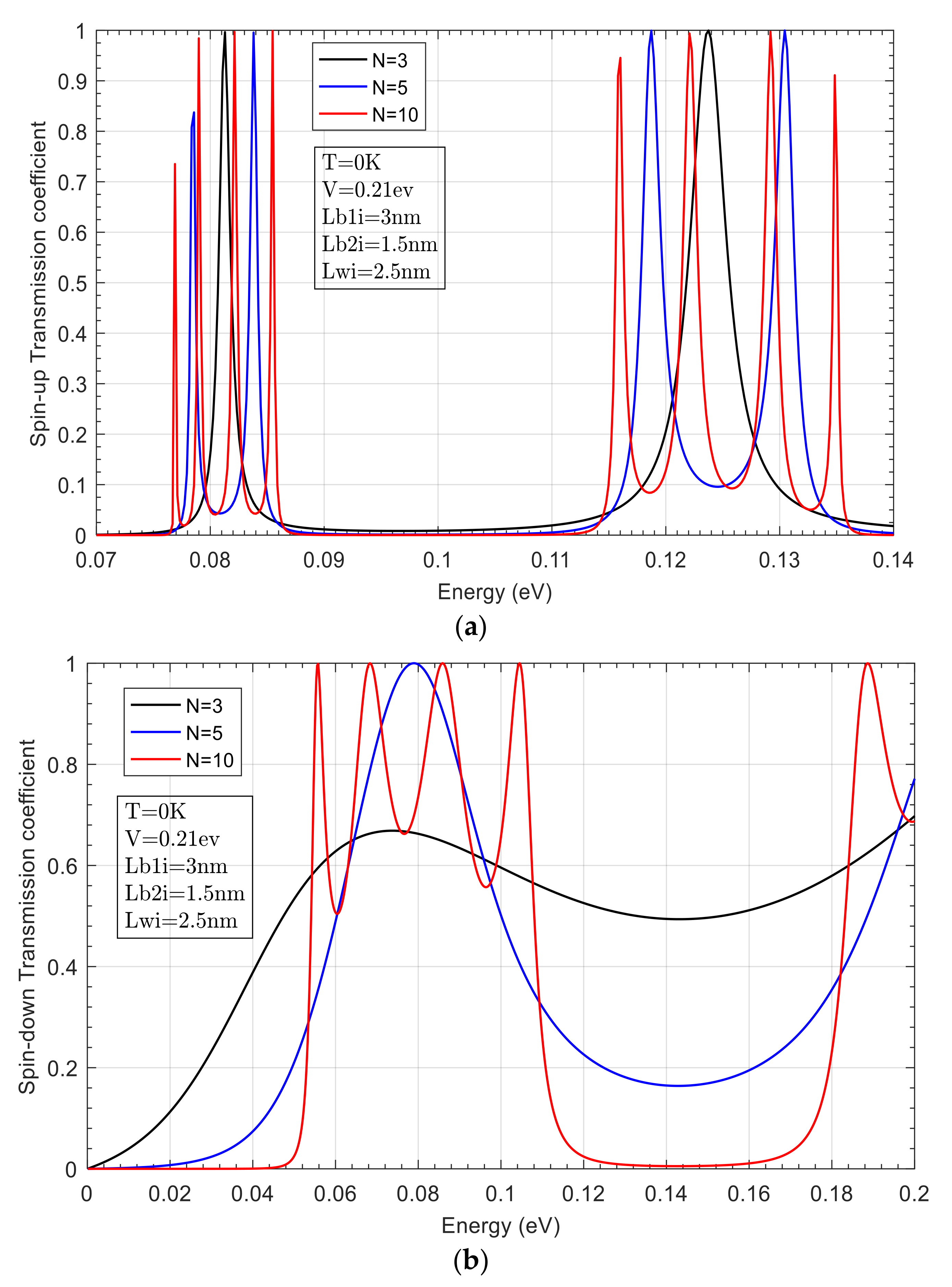
3.1. Electronic Transmission in Symmetric Structure

We begin our simulation by considering N-DMS layers Ga(1 − x)MnxAs alternated by nonmagnetic GaAs layers. The magnetic layers have equal widths Lbi = 1.5 nm. GaAs layers also have the same width Lwi = 2.5 nm. The structure is considered a symmetric one, as shown in Figure 2. We consider in this case three values of temperatures: (T = 0, 80 and 100 K) and three numbers of barriers (N = 3, 5 and 10 barriers). Figure 3a shows the variation of spin-up transmission coefficient Tup (E) as a function of the incident energy. The temperature is equal to T = 0. By examining this figure, we remark that the transmission coefficient presents a lot of resonant states. For instance, we observe only two resonant states for (N = 3). However, it becomes four states for (N = 5) and nine states for (N = 10). In other words, we obtain (N-1) peaks if we consider N barriers. This result is important since it permits us to adjust the desired number of resonant states by selecting the suitable number of magnetic barriers. In addition, we observe that all the transmission coefficients have approximately the same starting energy (0.06 eV) regardless of the number of barriers.
In Figure 3b, we plot the spin-down transmission Tdown (E) as a function of incident energy. We considered the same parameters as in Figure 3a. We remark that the transmission coefficients present less resonant states compared to the previous case of spin-up holes. As N increases, the resonant states shift to lower energies.
Furthermore, the transmission coefficients present different starting points for different values of N. For low energies (E less than 0.1 eV), Tdown (E) values are extremely small, and the structure is opaque for holes regardless of the number of barriers. However, it becomes transparent, and Tdown (E) can reach the unity for higher incident energies. These results can be used in consideration in the realization of spin filters based on multi-magnetic barriers.
To give a complete idea of the effect of temperature on the hole’s transmission, in Figure 4a, b, we plot the transmission coefficients as a function of the incident energy for a temperature equal to T = 80 K. The transmission coefficient for spin-up holes Tup (E) presents some oscillations indicating the existence of resonant states. These oscillations start from an energy E = 0.05 eV. In other words, the increase of the temperature shifts the resonant states toward lower energies. This shift towards lower energies is clearer for spin-down holes. In fact, as shown in Figure 3b, Tdown (E) starts its oscillation at E = 0 eV regardless of the number of barriers. We also remark that the domain of oscillation [0–0.05 eV] was forbidden at temperature T = 0 K (Figure 3b). Consequently, the high temperature produces additional oscillations, especially in lower incident energies.
Finally, the variations of Tdown (E) and Tup (E) as a function of the incident energy for T = 100 K are plotted in Figure 5a, b. By examining these figures, we note two opposite behaviors. For the spin-up holes, the number of oscillations is reduced. However, that of spin-down holes is increased. In other words, Tdown (E) presents more oscillations for T = 100 K compared to the previous temperatures. For instance, if we examine Tdown (E) for N = 10, it presents four peaks for T = 100 K, but in the case of T = 80 K, it presents only three resonant states. N = 5 presents only one resonant state for T = 80 K, but it shows two states at T = 100 K. This important result can be used to adjust the desired spin polarization of holes and by selecting the suitable temperature of the system.

3.2. Electronic Transmission in an Asymmetric Structure

In this section, we study the asymmetry of the structure and discuss its impact on the transmission coefficients Tup (E) and Tdown (E). The structure has the same number of layers as shown in the previous section, but the widths of magnetic (GaMnAs) and nonmagnetic (GaAs) layers are different. We fix the width of the layers as following: Lb1i = 3 nm, Lb2i = 1.5 nm, and Lwi = 2.5 nm (Figure 6).
In this section, the temperature is fixed to T = 0 K. Figure 7a shows the variation of Tup (E) as a function of the incident energy for three barrier numbers. It is clear that Tup (E) presents some peaks indicating the existence of resonant states. We remark that the number of resonant states increases with the number of barriers. In addition, the transmission coefficient presents two series of resonance separated by a gap of energy. The first series is between 0.075 and 0.09 meV, and the second series is between 0.11 and 0.14 eV. The peaks of the first series are sharper than the second series. This phenomenon obtained by the asymmetric structure is very important since it indicates that the transmission can be turned off by selecting the appropriate incidence energies. In fact, the structure can be transparent for holes coming with energies corresponding to the first and second series of oscillations. However, it acts as a barrier for all energies situated inside the gap region.
The transmission coefficient of spin-down holes is displayed in Figure 7b. It is clear that many oscillations are obtained for N = 10 layers. Similarly, as in the case of spin-up holes, the transmission coefficient presents a gap of energy separating the two series of resonance. However, in this case, we have only a first series of oscillations. The second one starts at E = 0.18 eV. For a lower number of barriers (N = 5 and 3), the peaks become less sharp, and their number is reduced.
By comparing the results obtained in asymmetric and symmetric structures, we can conclude that asymmetricity introduces a different behavior in the transmission coefficients, such as the gap energy region which was absent in symmetric structures. In addition, in the asymmetric structure, the transmission coefficient presents a large number of maximums. These maximums are sharper compared to those obtained in symmetric cases. The number of resonant states is multiplied which constitutes an important finding for experimenters to select the suitable structure according to the number of resonant states.
In addition, we can note that the obtained results present great accordance with those obtained by Shi-Hsin Lin and Yong-Jin Cho [23]. In their investigation, they applied the same model to single magnetic layer GaMnAs sandwiched between two GaAs layers. The spin-up transmission coefficient presents some oscillations with sharp amplitudes, however, the spin-down transmission coefficient grows linearly and tends to unity without oscillation. This behavior of the transmission coefficient was found by our theoretical model in our previous published work [29] which confirms the validity of our calculation.

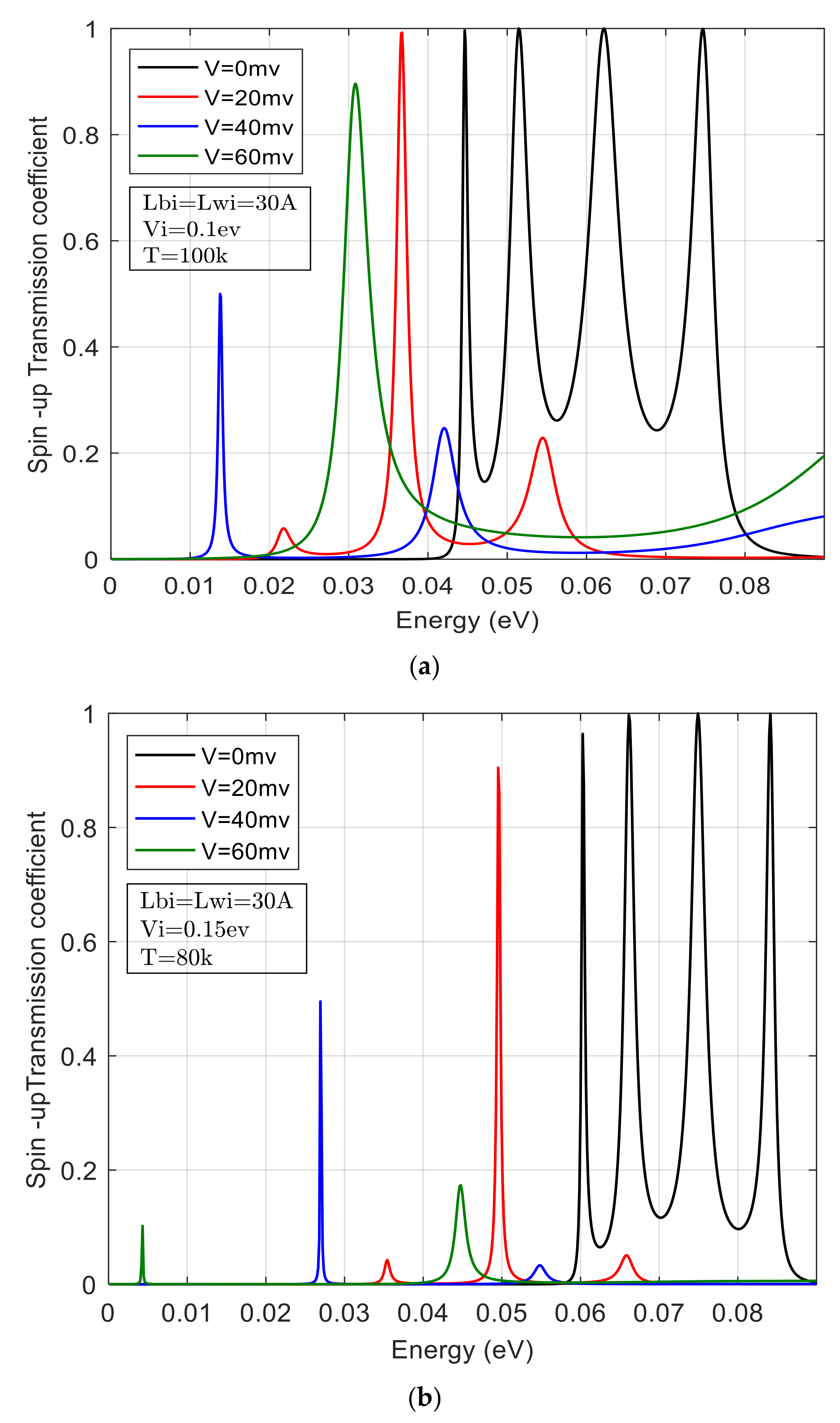
3.3. Effect of an Applied Bias Voltage on the Transmission Coefficient

In this section, we consider five Ga(1 − x)MnxAs layers (N = 5). The widths of DMS and GaAs layers are fixed to 3 nm (Figure 8). The applied bias voltage was taken as the principal parameter of the simulation. In Figure 9a, b, we draw the Tup (E) variation of the spin-up holes depending on the incident energy for four values of the applied voltages. In this case, we have only considered two different temperatures, T = 100, 80 K.
We notice that Tup (E) presents multi resonant states since it shows many peaks. At a fixed temperature, these peaks move leftwards by augmenting the voltage v. In fact, when we augment v, the quantum wells between barriers intensify their depths, leading to a huge diminishing of the values of the resonant state, and this introduces a shift of the peaks toward the lower energies. Furthermore, we observe from these figures that the amplitudes of Tup(E) coefficients are reduced by increasing the bias voltage. For instance, as shown in Figure 9a, the maximum of Tup(E), which is equal to one for v = 0 volts, is then reduced to 0.9 for v = 60 mV.
In addition, we remark on the importance of temperature on the transmission coefficients. In fact, when T increases, the maxima of the transmission coefficients shift towards lower energies regardless of the applied voltage value. Furthermore, the peaks of the transmission coefficients become sharper by reducing the temperatures. This behavior is very important since it acts on the holes’ tunneling time, which depends strongly on the width of resonant peaks.
The spin-down transmission variations depending on the incident energy for two distinct temperatures (T = 80 and 100 K) and various applied voltages are displayed in Figure 10a, b. We remark evidently that the Tdown (E) coefficients augment quasi-linearly with the incident energy less than 50 meV. For values greater than 50 meV, the Tdown (E) coefficients practically reach unity. In other words, the structure becomes completely transparent for the spin-down holes. This means that the structure is completely transparent for holes with energy levels higher than 50 meV. The saturation behavior observed in the transmission coefficient occurred for lower energies when we increase the intensity of the applied voltage. The perfect transmission of spin-down holes is because the magnetic layers, which act as barriers for spin-up holes, now act as quantum wells for spin-down holes. These wells accelerate the transmission of the spin-down holes. This explains the strong augmentation of spin-down coefficients, which touch the unity without a large number of oscillations.
In addition, we remark that at lower incident energies, the transmission coefficients have different values, but all of them tend to the unity for higher incident energies. In addition, we remark that by reducing the temperature, the transmission coefficient maintains the same shape, but the maximum of the transmission is attained for lower incident energies. For example, at T = 100 K, the transmissions coefficients reach unity for E larger than 80 mV. However, at T = 80, unity is obtained for energy equal to 60 mV.
The percentage of holes transmitted through the structure can be evaluated by calculating the spin-polarization P(E), which depends on the incident energy. To do this, we display in Figure 11a, b the spin-polarizations for different temperatures. We notice that P(E) rises from −1 and intensifies gradually until it touches a maximum and then diminishes. In addition, it is clear that P(E)max shifts to lower energies when we increment the voltage. The spin-up transmission is suppressed at small incident energies, and the spin-down transmission is predominant. However, for high incident energies, the polarization augments, and the spin-up holes can be completely transmitted through the structure, especially when the incident energy is equal to one of the resonant energy levels of the system. Additionally, we remark that at T = 80 K, the P(E) occurs for low incident energy compared to the case when T is equal to 100 K and for high applied voltage (V = 60 mV).
Figure 12a, b shows the variations of the spin-up and down current densities produced by five magnetic barriers (N = 5) as a function of the applied voltage for various temperatures. It appears that the spin-up current density begins at zero and grows gradually until it touches its maximum and then declines.
Furthermore, we notice that the higher amplitude of the current occurred at high temperatures. For example, the highest current density J max = 5 × 10 3 ( u . a . ) is obtained at T = 60 K, but this value is equal to 9 × 10 3 ( u . a . ) at T = 80 K. This result is important since it permits the experimenter to obtain the desired current by selecting a suitable temperature.
Note, that a significant physical phenomenon is presented in Figure 12a. This physical phenomenon is the negative differential resistance (NDR). In fact, after the current reaches its maximum, it declines and continues to decrease, presenting a negative slope, leading to an (NDR) resistance that is beneficial for many spintronics applications.
The spin-down current density depending on the applied bias voltage for different temperatures is displayed in Figure 12b. It is clear that the spin-down current density rises progressively until it reaches a certain maximum and then decreases. Furthermore, we observe that it presents some oscillations due to the existence of resonant states discussed in the previous section. In this case (spin-down), the (NDR) region is less important than that produced by the spin-up current. However, at low-temperature (T = 20 K), we observe that the current density starts from its maximum and diminishes slowly.

4. Conclusions

We have investigated the impact of the temperature and an externally applied bias voltage on transmission coefficients for holes (spin-up and down) in a diluted magnetic semiconductor multi-barrier GaMnAs/GaAs using the (TMM) approach. We have considered the effect of the asymmetry of the spin-dependent confining potential on the transmission coefficients by tuning the temperature and the widths of the (DMS) layers. We show that these coefficients present an oscillating behavior due to the resonant states and strongly depend on the temperature of the system and the number of magnetic layers. Furthermore, it is shown that these states are multiplied, and they moved to lower energies for spin-up and down holes by increasing the number of (DMS) layers. We have also noticed that the asymmetric structure is very important since it indicates that the transmission can be turned off by selecting the appropriate energies of incidence. Afterward, we have calculated the spin-up and down current densities through five magnetic barriers, and the obtained results justify the existence of NDR regions in spin current densities. These NDR regions are more important for spin-up holes than spin-down holes. The obtained results are beneficial to manufacturing high-speed spin-filters and diodes by selecting the appropriate applied voltage and temperature values. Furthermore, the transmission coefficient and the spin polarization behaviors can be tuned by selecting the suitable values of incident energy of holes that permits it to reach high transmission. Thus, it is practical to design and fabricate optoelectronic devices based on the proposed heterostructures.

Author Contributions

Conceptualization, N.S.A.-S. and H.D.; Formal analysis, N.S.A.-S. and H.D.; Investigation, N.S.A.-S. and H.D.; Software, N.S.A.-S. and H.D.; Writing–original Draft, N.S.A.-S. and H.D. All authors have read and agreed to the published version of the manuscript.

Funding

There is no external funding.

Institutional Review Board Statement

Not applicable.

Informed Consent Statement

Not applicable.

Data Availability Statement

Data are contained within the article.

Conflicts of Interest

The authors declare no conflict of interest.

References

  1. Ohno, H.; Munekata, H.; Penney, T.S.; Molnár, V.; Chang, L.L. Magnetotransport properties of p-type (In,Mn)As diluted magnetic III-V semiconductors. Phys. Rev. Lett 1992, 68, 2664–2667. [Google Scholar] [CrossRef] [PubMed]
  2. Ohno, H. Making Nonmagnetic Semiconductors Ferromagnetic. Science 1998, 281, 951–956. [Google Scholar] [CrossRef] [PubMed]
  3. Ohno, H. Properties of ferromagnetic III–V semiconductors. J. Magn. Magn. Mater. 1999, 200, 110–129. [Google Scholar] [CrossRef]
  4. Sadowski, J.; Kret, P.D.S.; Janik, E.; Łusakowska, E.; Kanski, J.; Tang, D. GaAs: Mn nanowires grown by molecular beam epitaxy of (Ga, Mn) As at MnAs segregation conditions. Nano Lett. 2007, 7, 2724–2728. [Google Scholar] [CrossRef] [PubMed] [Green Version]
  5. Borschel, C.; Messing, M.E.; Borgström, M.T.; Paschoal, W., Jr.; Wallentin, J.; Kumar, S.; Ronning, C. A new route toward semiconductor nanospintronics: Highly Mn-doped GaAs nanowires realized by ion-implantation under dynamic annealing conditions. Nano Lett. 2011, 11, 3935–3940. [Google Scholar] [CrossRef] [PubMed]
  6. Kumar, S.; Paschoal, W., Jr.; Johannes, A.; Jacobsson, D.; Borschel, C.; Pertsova, A.; Pettersson, H. Magnetic polarons and large negative magnetoresistance in GaAs nanowires implanted with Mn ions. Nano Lett. 2013, 13, 5079–5084. [Google Scholar] [CrossRef]
  7. Hilse, M.; Takagaki, Y.; Herfort, J.; Ramsteiner, M.; Herrmann, C.; Breuer, S.; Geelhaar, L.; Riechert, H. Ferromagnet-semiconductor nanowire coaxial heterostructures grown by molecular-beam epitaxy. Appl. Phys. Lett. 2009, 95, 133126. [Google Scholar] [CrossRef]
  8. Dellas, N.S.; Liang, J.; Cooley, B.J.; Samarth, N.; Mohney, S.E. Electron microscopy of GaAs/MnAs core/shell nanowires. Appl. Phys. Lett. 2010, 97, 072505. [Google Scholar] [CrossRef]
  9. Sadowski, J.; Siusys, A.; Kovacs, A.; Kasama, T.; Dunin-Borkowski, R.E.; Wojciechowski, T.; Kowalski, B. GaAs–MnAs nanowires. Basic Solid State Phys. 2011, 248, 1576–1580. [Google Scholar] [CrossRef]
  10. Rudolph, A.; Soda, M.; Kiessling, M.; Wojtowicz, T.; Schuh, D.; Wegscheider, W.; Reiger, E. Ferromagnetic GaAs/GaMnAs core− shell nanowires grown by molecular beam epitaxy. Nano Lett. 2009, 9, 3860–3866. [Google Scholar] [CrossRef] [Green Version]
  11. Siusys, A.; Sadowski, J.; Sawicki, M.; Kret, S.; Wojciechowski, T.; Gas, K.; Story, T. All-wurtzite (In, Ga) As-(Ga, Mn) As core–shell nanowires grown by molecular beam epitaxy. Nano Lett. 2014, 14, 4263–4272. [Google Scholar] [CrossRef] [PubMed] [Green Version]
  12. Ohno, Y.; Young, D.K.; Beschoten, B.; Matsukura, F.; Ohno, H.; Awschalom, D.D. Electrical spin injection in a ferromagnetic semiconductor heterostructure. Nature 1999, 402, 790–792. [Google Scholar] [CrossRef]
  13. Ohno, H.; Akiba, N.; Matsukura, F.; Shen, A.; Ohtani, K.; Ohno, Y. Spontaneous splitting of ferromagnetic (Ga, Mn) As valence band observed by resonant tunneling spectroscopy. Appl. Phys. Lett. 1998, 73, 363–365. [Google Scholar] [CrossRef]
  14. Koshihara, S.; Oiwa, A.; Hirasawa, M.; Katsumoto, S.; Iye, Y.; Urano, C.; Takagi, H.; Munekata, H. Ferromagnetic Order Induced by Photogenerated Carriers in Magnetic III-V Semiconductor Heterostructures of (In,Mn)As/GaSb. Phys. Rev. Lett. 1997, 78, 4617–4620. [Google Scholar] [CrossRef]
  15. Oiwa, A.; Mitsumori, Y.; Moriya, R.; Słupinski, T.; Munekata, H. Effect of optical spin injection on ferromagnetically coupled Mn spins in the III-V magnetic alloy semiconductor (G a, M n). As. Phys. Rev. Lett. 2002, 88, 137202. [Google Scholar] [CrossRef]
  16. Egues, J.C. Spin-Dependent Perpendicular Magnetotransport through a Tunable ZnSe/Zn 1− x Mn x Se Heterostructure: A Possible Spin Filter? Phys. Rev. Lett. 1998, 80, 4578. [Google Scholar] [CrossRef]
  17. Dietl, T.; Ohno, H.; Matsukura, F.; Cibert, J.; Ferrand, D. Zener Model Description of Ferromagnetism in Zinc-Blende Magnetic Semiconductors. Science 2000, 287, 1019–1022. [Google Scholar] [CrossRef] [Green Version]
  18. König, J.; Lin, H.H.; MacDonald, A.H. Theory of diluted magnetic semiconductor ferromagnetism. Phys. Rev. Lett. 2000, 84, 5628. [Google Scholar] [CrossRef] [Green Version]
  19. Saffarzadeh, A.; Shokri, A.A. Quantum theory of tunneling magnetoresistance in GaMnAs/GaAs/GaMnAs heterostructures. J. Magn. Magn. Mater. 2006, 305, 141–146. [Google Scholar] [CrossRef] [Green Version]
  20. Tao, Y.C.; Hu, J.G.; Liu, H. Spin-polarized transport in diluted GaMnAs/AlAs/GaMnAs ferromagnetic semiconductor tunnel junctions. J. Appl. Phys. 2004, 96, 498–502. [Google Scholar] [CrossRef]
  21. Ju, Y.; Shen, R.; Zheng, Z.M.; Xing, D.Y. The tunneling magnetoresistance in GaMnAs/GaAs/GaMnAs junctions. Phys. Lett. A 2007, 371, 327–331. [Google Scholar] [CrossRef]
  22. Jungwirth, T.; König, J.; Sinova, J.; Kučera, J.; MacDonald, A.H. Curie temperature trends in (III, Mn) V ferromagnetic semiconductors. Phys. Rev. B 2002, 66, 012402. [Google Scholar] [CrossRef] [Green Version]
  23. Lin, S.-H.; Cho, Y.-J. Spin Transport through GaAs/GaMnAs/GaAs. 2006. Available online: https://scholar.google.com/citations?view_op=view_citation&hl=en&user=3hC8vUgAAAAJ&pagesize=80&sortby=pubdate&citation_for_view=3hC8vUgAAAAJ:FPJr55Dyh1AC (accessed on 1 March 2022).
  24. Dakhlaoui, H.; Nefzi, M.; Al-Shameri, N.S.; Al Suwaidan, H.; Elmobkey, H.; Almansour, S.; Alnaim, I. Spin-polarized transmission across heterostructure based on an InAs/GaSb/InGaAs system: Effect of accelerating quantum wells. Chem. Phys. Lett. 2020, 757, 137866. [Google Scholar] [CrossRef]
  25. Dakhlaoui, H.; Nefzi, M.; Al-Shameri, N.S.; Al Suwaidan, A.; Elmobkey, H.; Almansour, S.; Alnaim, I. Magnetic field effect on spin-polarized transport in asymmetric multibarrier based on InAs/GaAs/GaSb systems. Phys. B Condens. Matter. 2020, 597, 412403. [Google Scholar] [CrossRef]
  26. Dakhlaoui, H. Magnetic Field and Hydrostatic Pressure Effects on Electron Transport in Heterostructure Based on InAs/GaAs Triple Barriers with Dresselhaus Interaction. Arab. J. Sci. Eng. 2021, 46, 5969–5975. [Google Scholar] [CrossRef]
  27. Tsu, R.; Esaki, L. Tunneling in a finite superlattice. Appl. Phys. Lett. 1973, 22, 562–564. [Google Scholar] [CrossRef]
  28. Al-Shameri, N.S.; Dakhlaoui, H.; Almansour, S.; Alnaim, I. Spin-Dependent Tunneling of Holes in Heterostructures Based on GaMnAs Semiconductor: Effects of Temperature and Quantum Size. J. Supercond. Nov. Magn. 2020, 33, 2143–2148. [Google Scholar] [CrossRef]
  29. Najla, S.; Al-Shameri, H.D. Physica B Condens. Matter 2022, 628, 413555. [Google Scholar]
Figure 1. Potential profile of GaAs/Ga1 − xMnxAs multibarrier structure.
Coatings 12 00504 g001
Figure 2. GaAs/Ga1 − xMnxAs/GaAs symmetric structure, (Lbi = 1.5 nm, Lwi = 2.5 nm).
Coatings 12 00504 g002
Figure 3. (a): The transmission coefficient of spin-up holes as a function of incident energy for three barrier numbers (N = 3, 5, and 10). (b) T = 0 K. Transmission coefficient of spin-down holes as a function of incident energy for three barriers numbers (N = 3, 5 and 10). T = 0 K.
Coatings 12 00504 g003
Figure 4. (a): The transmission coefficient of spin-up holes as a function of incident energy for three barrier numbers (N = 3, 5, and 10). T = 80 K. (b): The transmission coefficient of spin-up holes as a function of incident energy for three barrier numbers (N = 3, 5, and 10). T = 80 K.
Coatings 12 00504 g004
Figure 5. (a): The transmission coefficient of spin-up holes as a function of incident energy for three barrier numbers (N = 3, 5, and 10). T = 100 K. (b): The transmission coefficient of spin-up holes as a function of incident energy for three barrier numbers (N = 3, 5, and 10). T = 100 K.
Coatings 12 00504 g005
Figure 6. GaAs/Ga1 − xMnxAs/GaAs asymmetric structure (Lb1i = 3 nm, Lb2i = 1.5 nm, and Lwi = 2.5 nm).
Coatings 12 00504 g006
Figure 7. (a): The transmission coefficient of spin-up holes as a function of incident energy for three barrier numbers (N = 3, 5, and 10). T = 0 K. (b): The transmission coefficient of spin-up holes as a function of incident energy for three barrier numbers (N = 3, 5, and 10). T = 0 K.
Coatings 12 00504 g007
Figure 8. GaAs/Ga1 − xMnxAs/GaAs system, (Lwi = Lbi = 3 nm), N = 5.
Coatings 12 00504 g008
Figure 9. (a): Transmission coefficient of spin-up holes as a function of incident energy for different applied bias voltages (N = 5 and T = 100 K). (b): The Transmission coefficient of spin-up holes as a function of incident energy for different applied bias voltages (N = 5 and T = 80 K).
Coatings 12 00504 g009
Figure 10. (a): The transmission coefficient of spin-down holes as a function of incident energy for different applied bias voltages (N = 5 and T = 100 K). (b): The transmission coefficient of spin-down holes as a function of incident energy for different applied bias voltages (N = 5 and T = 80 K).
Coatings 12 00504 g010
Figure 11. (a): Spin-polarization as a function of incident energy for different applied bias voltages (N = 5 and T = 100 K). (b): Spin-polarization as a function of incident energy for different applied bias voltages (N = 5 and T = 80 K).
Coatings 12 00504 g011
Figure 12. (a): Spin-up current density as a function of applied bias voltages for different temperatures (N = 5). (b): Spin-down current density as a function of applied bias voltages for different temperatures (N = 5).
Coatings 12 00504 g012
Publisher’s Note: MDPI stays neutral with regard to jurisdictional claims in published maps and institutional affiliations.

