Article

Chemical Bath Deposited Orthorhombic SnS Films for Solar Cell Applications

by
Carlos Ocampo-Ortega
1,
Ines Riech
1,*,
Arturo Abelenda
1,
Ricardo Mis-Fernández
2,
Patricia Rodríguez-Fragoso
3 and
Julio Mendoza-Alvarez
3
1
Materials Science Laboratory, Faculty of Engineering, Autonomous University of Yucatan, Merida 97130, Mexico
2
Applied Physics Department, Cinvestav-IPN, Merida 97310, Mexico
3
Physics Department, Cinvestav-IPN, Mexico City 07360, Mexico
*
Author to whom correspondence should be addressed.
Coatings 2022, 12(2), 283; https://doi.org/10.3390/coatings12020283
Submission received: 25 January 2022 / Revised: 10 February 2022 / Accepted: 15 February 2022 / Published: 21 February 2022
(This article belongs to the Special Issue Optical Thin Film and Solar Cells)

Abstract

:
Tin sulfide (SnS) thin films were deposited by the chemical bath deposition technique. The used procedure allows us to obtain orthorhombic SnS in 3.5 h and achieve thicknesses of 390 nm. We study the influence of deposition times, percentage of Sn precursor, and post-annealing on the structural and optical properties. The X-ray diffraction measurements of SnS films prepared at a deposition time of 3 h showed orthorhombic structure with characteristic peaks of SnS2. However, increasing the deposition time and the Sn precursor, the orthorhombic SnS phase in these samples becomes predominant. Thin-film morphologies and thicknesses were identified by scanning electron microscopy (SEM). An increase in bandgap from 1.41 eV to 1.56 eV was observed by increasing Sn precursor. The optical properties remain constant after air annealing of 285 °C. Low-temperature photoluminescence spectra show emission bands at 2.5 eV attributed to the presence of SO2. Other deep level transitions were observed at about 0.9 eV, probably due to oxygen.

1. Introduction

Tin sulfide (SnS) is considered a promising absorber layer for Cd-free thin-film solar cells due to its excellent optoelectronic properties. Moreover, SnS is a binary compound semiconductor composed of non-toxic and earth-abundant materials. Its bandgap (1.3–1.4 eV) is near to the optimum range of 1.3–1.5 eV, and its absorption coefficient is appreciably high in the visible region (>104 cm−1) [1,2]. Although its theoretical energy conversion efficiency (η) is nearly 32%, at par with crystalline silicon solar cells [3], at present, the conversion efficiency record of SnS based solar cells is only 4.63% [4]. Therefore, a better understanding of the structural, chemical, and physical characteristics of SnS is required to achieve higher efficiencies.
The SnS compound usually possesses an orthorhombic crystal structure at room temperature and pressure with a = 0.432, b = 1.12, and c = 0.398 nm (JCPDS card No: 39-0354) lattice parameters. The different elemental compositions of tin and sulfur can form several binary compounds such as SnS, SnS2, Sn2S3, and other phases [5]. The simultaneous presence of these phases in tin sulfide films can affect their electrical and optical characteristics. For example, when a p-type phase (SnS) and an n-type phase (SnS2, Sn2S3,or both simultaneously) co-exist could result in an inversion of the conductivity type [6].
SnS thin films have been fabricated by different methods such as thermal evaporation [7], radio frequency (RF) sputtering [8], electron beam evaporation [9], chemical vapor deposition [10], successive ionic layer deposition [11], atomic layer deposition (ALD) [4], electrochemical deposition [12,13], and chemical spray pyrolysis [14,15]. To date, the best reported efficiency has been by the slow and expensive atomic layer deposition (ALD) process. Chemical bath deposition (CBD) has been reported to be a promising alternative method [16,17,18,19,20,21,22] because of its simplicity, low cost, and the possibility of obtaining large-area films. In CBD, the formation of the film takes place when the ionic product exceeds the solubility product. However, optimization of growth conditions, such as deposition time and solution concentration, is essential to avoid unnecessary precipitation, loss of materials during the deposition process, and the appearance of unwanted secondary phases of tin sulfide [23].
This work uses a method first reported in 2021 [24] that allows us to grow orthorhombic SnS thin films of 390 nm in 3.5 h. There are reported methods to obtain orthorhombic SnS by CBD with deposition times of 8, 17, 24, 30, and up to 40 h [20,21,25,26,27] and just a few with times below 6 h [28,29,30]. We study the effect of deposition time and percentage of Sn precursor on structural and optical properties of SnS thin films. Our main goal is to study the conditions in the growth process by CBD of tin monosulfide (SnS) thin film to obtain the best quality of the film and avoid post-growth treatments.
This work is based on a method first reported in 2021 [24], which focuses on studying the PH effect on the chemical deposited SnS films, using a deposition time of 3 h. It is important to note that the reported methods to obtain orthorhombic SnS by CBD use deposition times of 8, 17, 24, 30, and up to 40 h [20,21,25,26,27] and just a few use times below 6 h [28,29,30]. In the work of Higareda et al. [24], they observed a sulfur excess in the chemical solution when the amount of tin precursor was varied in percentages lower than 5%. Thus, to obtain SnS thin films with better crystallinity and stoichiometry, we focused on investigating the effect of the tin precursor increase. Additionally, we varied the deposition time in order to obtain thicker layers. The used procedure allowed us to grow single-phase orthorhombic SnS thin films of 390 nm in 3.5 h. The structural, morphological, and optical properties of SnS thin films were studied as a function of deposition time, percentage of Sn precursor, and thermal treatments. The photoluminescence technique was used to identify recombination mechanisms that could affect the performance of the SnS thin film as an absorber layer in a solar cell.

2. Materials and Methods

SnS thin films were prepared using the chemical bath that contained 0.564 g of tin chloride (SnCl2·H2O) as the tin precursor, 1.697 g of ammonium citrate ( C 6 H 17 N 3 O 7 ) as complexing agent, and 0.617 g of sodium thiosulfate ( Na 2 S 2 O 3 · 5 H 2 O ) as sodium precursor.
Soda-lime glasses used as substrates were cleaned in subsequent ultrasonic baths (liquid soap, deionized water, acetone, and methanol). Afterwards, they were rinsed with deionized water and dried with nitrogen. Initially, the chemical bath showed a dark brown appearance and changed to dark brown with increasing time. The deposition time and tin precursor concentration used in the deposition process is shown in Table 1. The most homogeneous and hole-free deposited faces of the substrates were selected using a light source behind the sample and varying the viewing angle. The selected face was cleaned with deionized water for further characterization.
Post-growth thermal annealing was performed in all samples to verify the thermal stability. The parameters for the annealing were defined as presented by Ristov et al. [31], heating the samples to 285 °C for 30 min in an air atmosphere.
The crystal structure was characterized by grazing incidence X-ray diffraction (XRD, SIEMENS, Munich, Germany). Spectra were obtained using a Siemens D5000 diffractometer with an incident angle of 1 degree; the measurement was performed in 2θ sweeping from 10 to 80 degrees with a scan speed of 0.02°/3 s using a Cu kα tube (λ = 1.5406 Å). Observations of the surface morphology were carried out using a JEOL JSM-7600F scanning electron microscope (SEM, JEOL, Tokio, Japan) with 2 kV of accelerating voltage. The optical transmittance measurements were made using a JASCO 670 spectrophotometer (JASCO, Portland, OR, USA). PL measurements were carried out at 20 K using a closed cycle He cryostat (SHI-APD Cryogenics Inc., London, UK). The samples were measured in the UV-VIS region using a 442 nm line of HeCd laser as the excitation source. In this case, the PL signal was detected using HRD-100 Jobin–Yvon double monochromator (HORIBA, Kyoto, Japan) and Ag–Cs–O Hamamatsu photomultiplier (HAMAMATSU, Hamamatsu, Japan). The infrared sample emission was obtained using a 488 nm Argon ion laser line and recorded by Acton monochromator (Laser physics, West Jordan, UT, USA) and InGaAs detector (HORIBA, Kyoto, Japan).

3. Results and Discussion

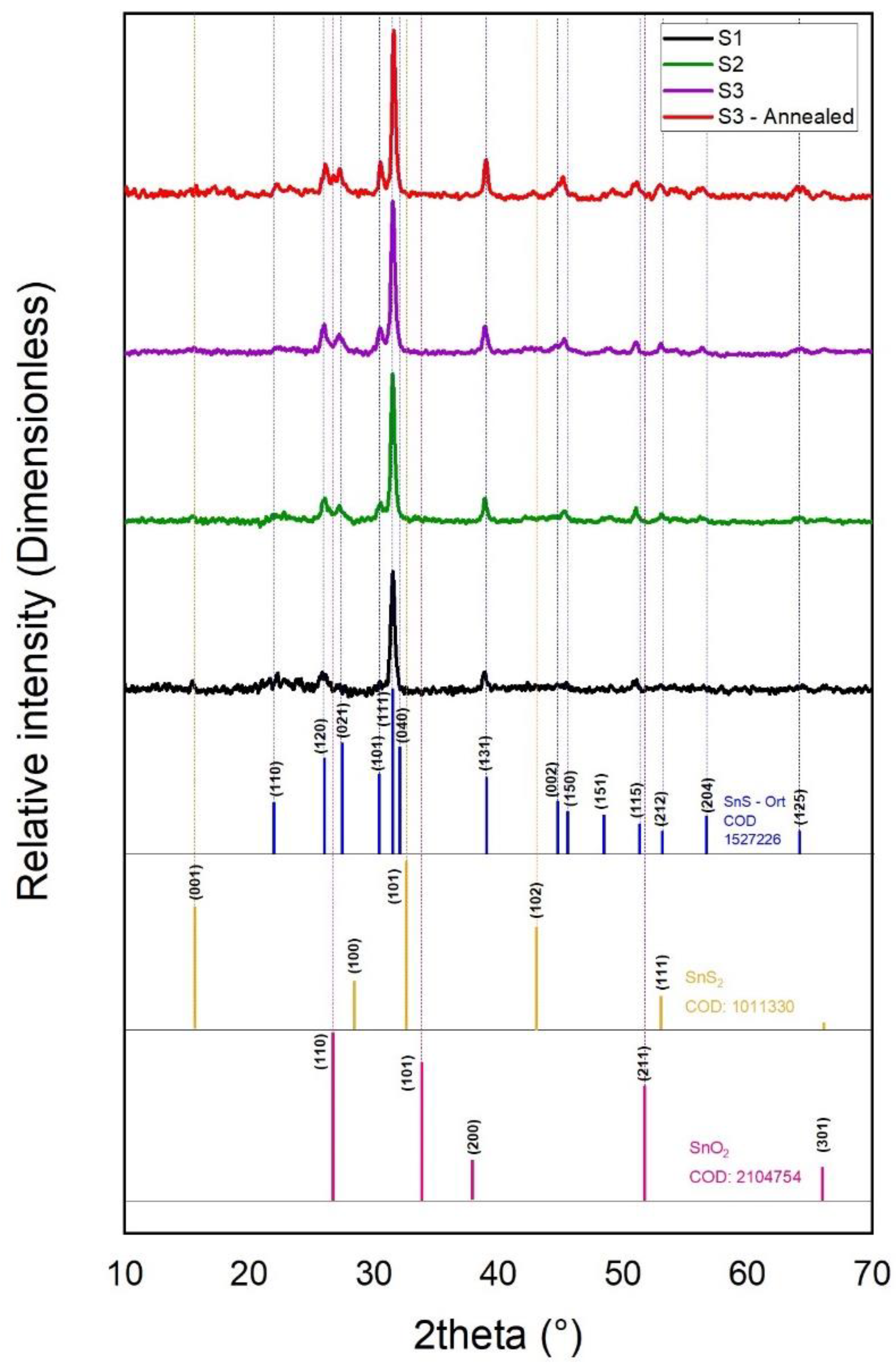
3.1. Structural Studies

Figure 1 shows the XRD pattern of the samples, which agrees with the typically reported structure of the orthorhombic SnS phase (reference COD #96-152-7226). Here, we could not notice any peak related to the trigonal SnS2 secondary phase (reference COD # 96-703-8081), except in sample S1, where a low-intensity peak in the (001) direction is observed [10,32]. In the figure, it can be seen that as the deposition time and the concentration of the Sn precursor increased, the peaks corresponding to the orthorhombic SnS phase were further accentuated. These effects, produced by the change of the growth conditions, could be indicating an improvement in the crystalline quality of the sample.
We determined the crystallites size (D) in the principal crystallographic direction (111) using Scherrer’s formula:
D = K · λ a · cos θ
where K is the form factor, λ is the wavelength of the X-ray source, θ is the angle of the Bragg reflection, and a is the full width at half medium (FWHM) of the diffraction peak in radians. In our case, the form factor used was K = 0.9 and λ = 1.5418 Å corresponding to the Kα line of copper. The results obtained can be seen in Table 1. We can observe that as the chemical bath time increased, the crystallite size also increased. While increasing the concentration of the Sn precursor, the crystallite size remained practically constant. This indicates that increasing the Sn precursor concentration during growth improves the quality of the crystalline structure, and the SnS orthorhombic phase formation is promoted. The diffractograms of sample S3 before and after the thermal annealing is shown in Figure 1. It can be noted that after the annealing, the XRD pattern remains almost unchanged, indicating that the main phase of SnS was not affected. This result agrees with the reported results in previous studies [24].

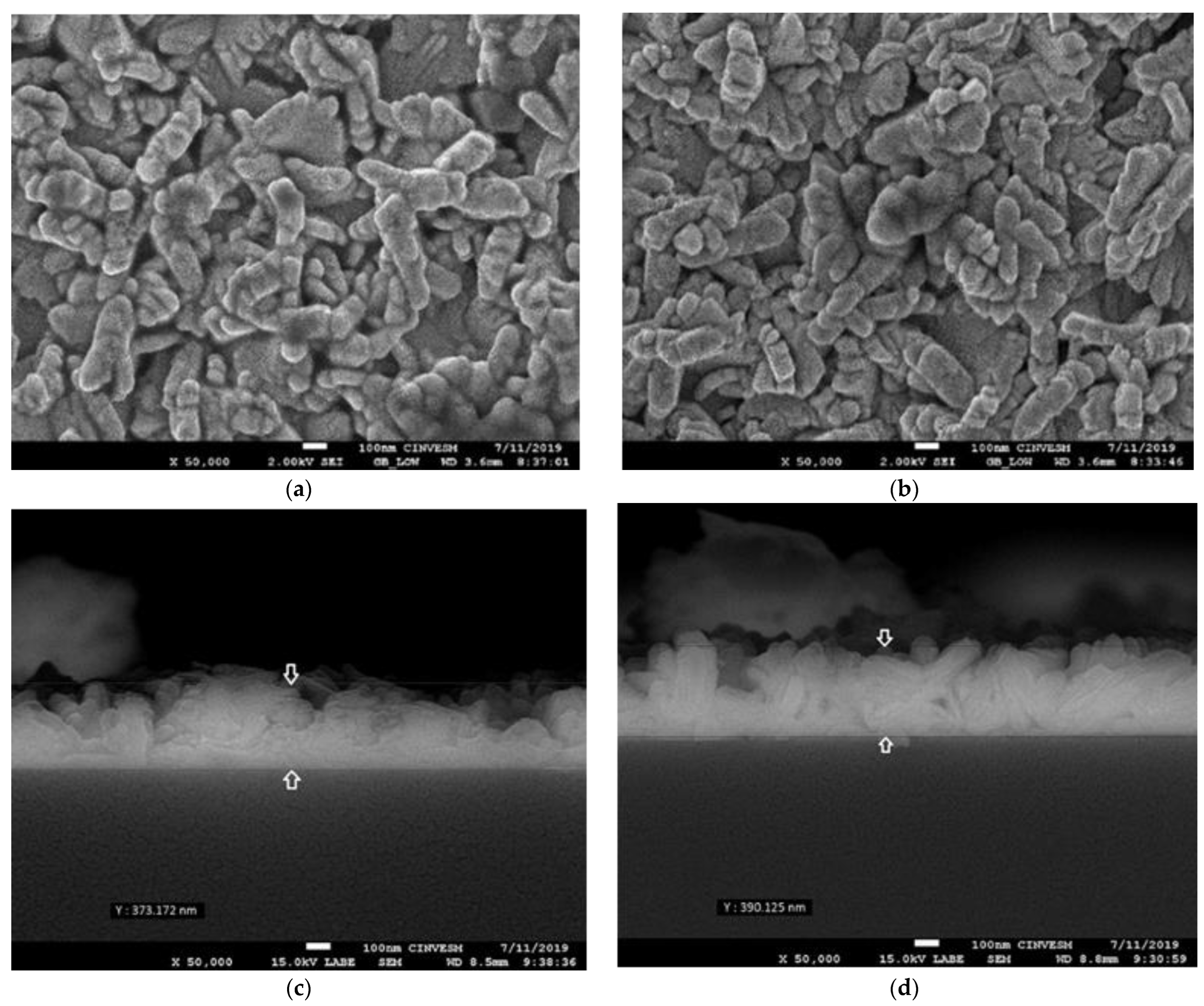
3.2. Morphological Studies

The thin films’ morphology was analyzed using scanning electron microscopy. The SEM image of sample S3, before and after the thermal annealing, is shown in Figure 2a,b. We can see elongated structures formed by smaller grains with an average size between 100 nm and 120 nm, respectively. This morphology has been previously reported for SnS thin films [33,34]. The figure shows a certain degree of coalescence between the grains and a compact bulk.
It should be noted that the annealing of the samples slightly increased the coalescence of the grains but did not affect the rest of the morphological characteristics of the samples. The thicknesses obtained from cross-sectional SEM images were 373 nm and 390 nm for S2 and S3 (see Figure 2c,d). For sample S1, the thickness value could not be obtained due to the low thickness of the sample, which was identified visually.

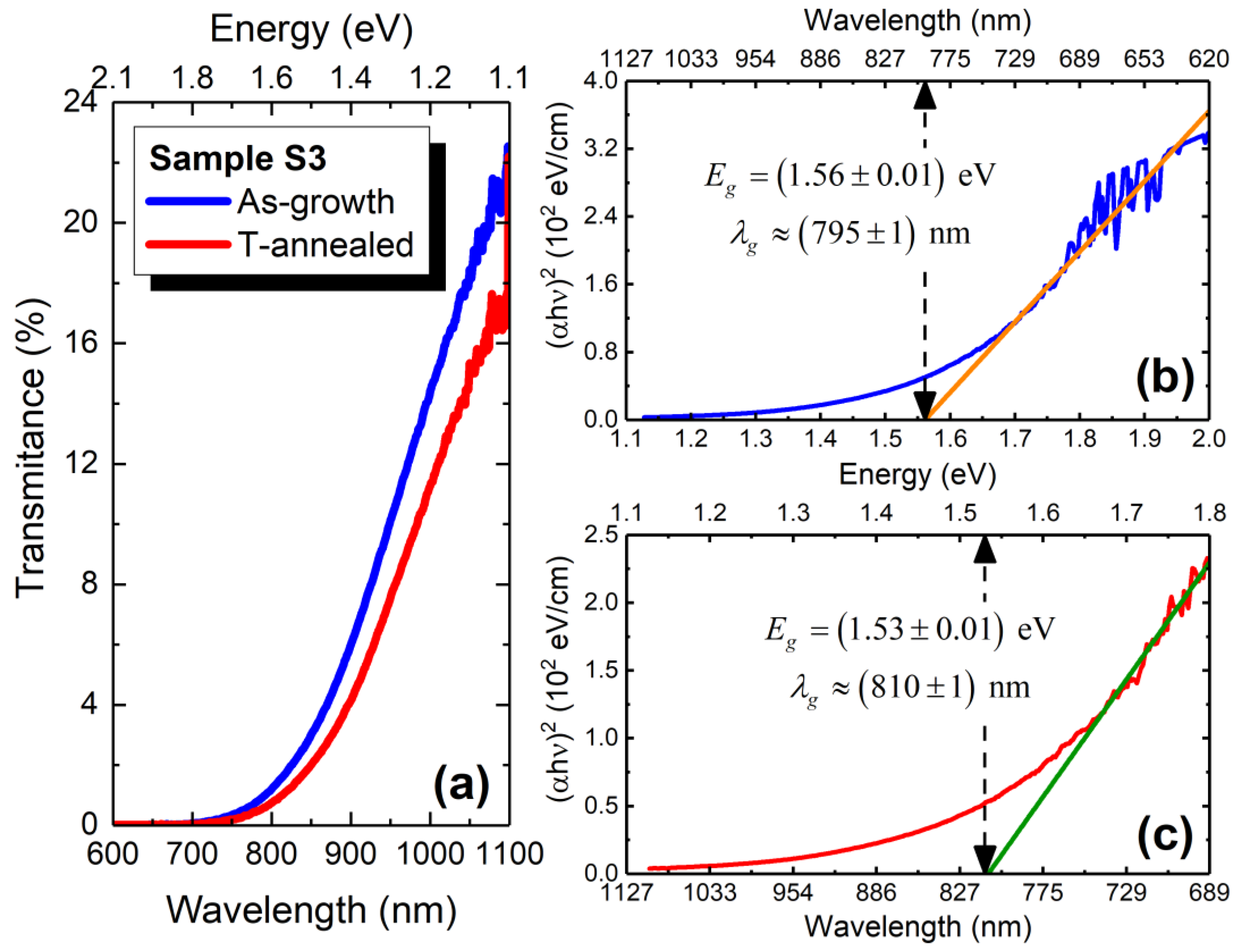
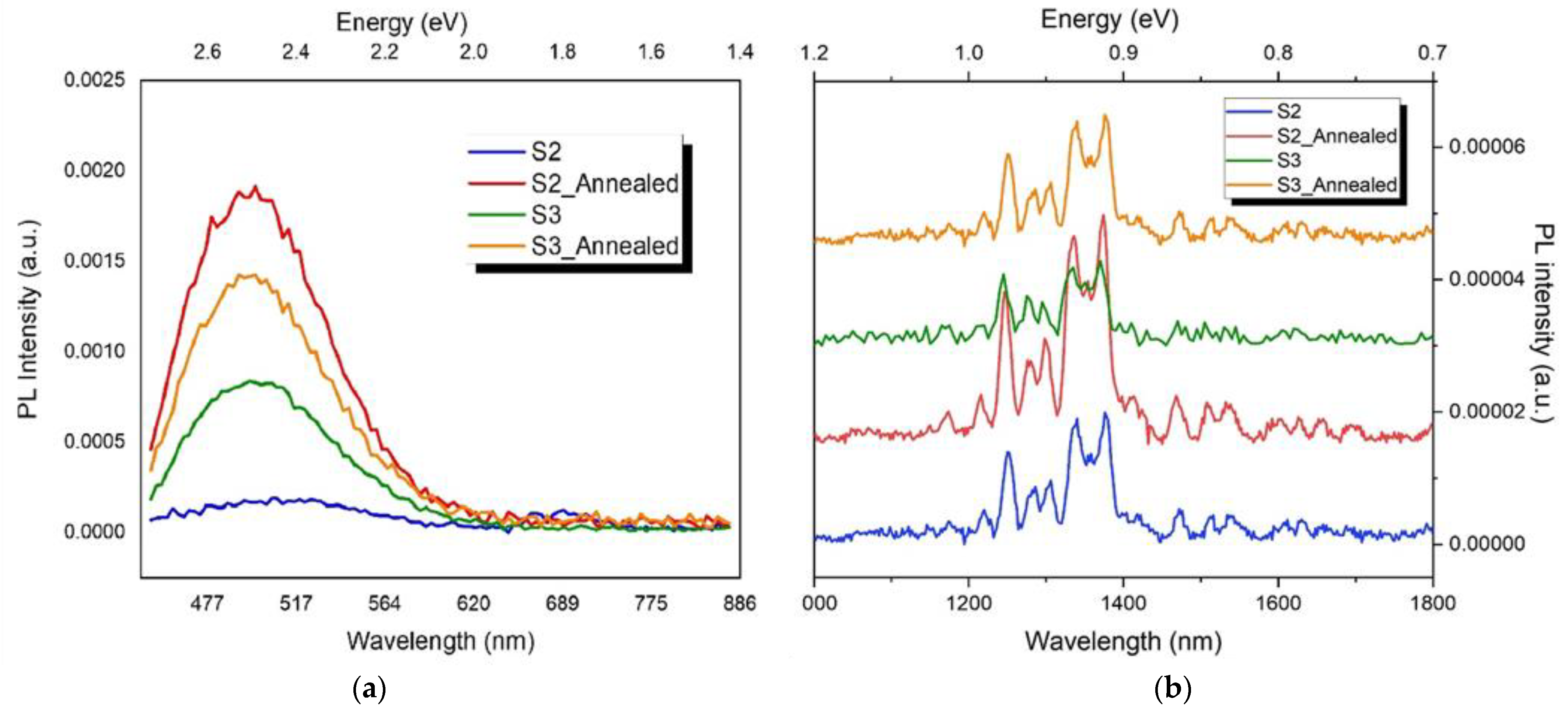
3.3. Optical Studies

To obtain the bandgap values, the optical transmittance for the as-deposited and annealed SnS films, samples S2 and S3, was recorded in the 400–1100 nm wavelength. Figure 3a shows the optical transmittance for sample S3 and the shift in the absorption edge after the annealing. Figure 3b,c shows the Tauc plot for sample S3 to determine the optical bandgap, using the expression:
( α hv ) 2 = A ( hv E g )
where is the absorption coefficient, Eg is the bandgap energy, h ν is the photon energy, and A is a constant. A linear region in the Tauc plot indicates direct gap material, with an estimated energy gap of 1.56 eV and 1.53 eV for sample S3 before and after annealing, respectively. The same procedure was applied to sample S2.
Table 2 summarizes the bandgap energies obtained for samples S2 and S3. In the case of sample S1, a conclusive result in the transmittance measurement could not be obtained due to the low sample thickness. Because of the lack of bandgap and thickness data for sample S1, we continue the subsequent optical studies only with S2 and S3.
The bandgap energy obtained for sample S2 (1.41 eV) agrees with the values reported in the literature for orthorhombic SnS deposits [2]. However, for sample S3, the bandgap energy is slightly higher. This can be explained considering that sample S3 is richer in Sn, which favors the formation of SnO2 due to the greater availability of Sn. Therefore, the optical bandgap of sample S3 increases (1.56 eV). Other authors have reported similar behavior after air annealing of SnS thin films [35]. This result is supported by the PL measurements presented in the Section 4 in Figure 4a. Table 2 also shows that heat treatment in both samples S2 and S3 does not modify its bandgap energy. They are similar if we consider the error values. This indicates that both samples are thermally stable, maintaining their optical properties.
Low-temperature PL spectroscopy was used to investigate the radiative recombination processes of SnS films. Most of the PL studies of SnS films reported in the literature are carried out in the visible range of the spectrum. However, there are very few reports on photoluminescence in the infrared region. Figure 4a shows PL spectra of S2 and S3 before and after annealing in the UV–Vis region with photon excitation at 442 nm. A broad and asymmetric band was observed around 2.50 eV for both samples. We associated this band with the SnO2 presence [31,36,37]. The peak corresponding to the Sn-rich sample, S3, has a higher PL intensity than S2 due to the greater formation of the oxide compound, as explained previously. After annealing, performed in an air atmosphere, the transformation of SnS into SnO2 is promoted by following the reaction [34].
2 SnS + O 2 SnO 2 + SnS 2
The formation of SnO2 can be explained by the oxidation of Sn(II) to Sn(IV).
We performed a PL study between 1000–1800 nm to observe deep-level states in SnS samples. Figure 4b displays PL spectra in the infrared region for samples excited at 488 nm. We can see a multi-peak emission between 0.90 eV and 0.99 eV. The bands’ intensity increased after annealing, suggesting that these emissions may be due to deep oxygen-related levels. This behavior was observed by Sajeesh et al. [33], whose reported deep-level transitions were attributed to the presence of oxygen. According to the results presented, sample S3, compared to samples S1 and S2, would be a better candidate for use in solar cells due to its better crystallinity of orthorhombic single phase without the need for post-deposition heat treatment. In addition, as mentioned above, deposition times from 6 h to 30 h have been reported in the literature. We use a method that allows us to grow SnS with thickness values close to that used in the recorded cell in shorter times. This has allowed us to work on bilayers for future applications in photovoltaic structures. Further studies are currently underway to determine the nature of the emissions found in the infrared range to optimize the film’s properties for use in photovoltaic structures.

4. Conclusions

SnS thin films with a thickness of 390 nm are deposited in 3.5 h at room temperature. The XRD analysis reveals orthorhombic structures with a low presence of the SnS2 phase. The study showed that as the deposition time and the concentration of the Sn precursor in the bath increased, the peaks corresponding to the orthorhombic SnS phase were further accentuated, indicating an improvement in the crystalline quality of the sample. However, greater availability of Sn leads to a more significant formation of SnO2 and a slightly higher optical bandgap. SEM images show that deposited films are homogenous, formed by smaller grains with an average size between 100 nm and 120 nm. PL characterization confirmed the presence of SnO2 through a band located around 2.4 eV, whose intensity increases with thermal treatment in air. PL emission bands were found in the infrared region, probably due to deep levels related to oxygen.

Author Contributions

Conceptualization, C.O.-O., I.R. and A.A.; validation, I.R., A.A. and R.M.-F.; formal analysis, C.O.-O. and A.A.; investigation, C.O.-O., R.M.-F. and P.R.-F.; writing—original draft preparation, C.O.-O. and A.A.; writing—review and editing, I.R. and J.M.-A. All authors have read and agreed to the published version of the manuscript.

Funding

This research was funded by CONACYT-SENER under contract 254667.

Institutional Review Board Statement

Not applicable.

Informed Consent Statement

Not applicable.

Data Availability Statement

Not applicable.

Acknowledgments

Carlos Ocampo-Ortega acknowledge the financial support by the CONACYT Postgraduate Scholarship. The authors thank LANNBIO CINVESTAV-Mérida for SEM measurements.

Conflicts of Interest

The authors declare no conflict of interest. The funders had no role in the design of the study; in the collection, analyses, or interpretation of data; in the writing of the manuscript; or in the decision to publish the results.

References

  1. Sohila, S.; Rajalakshmi, M.; Ghosh, C.; Arora, A.; Kand, M. Optical and Raman scattering studies on SnS nanoparticles. J. Alloys Compd. 2011, 509, 5843–5847. [Google Scholar] [CrossRef]
  2. Jacob, A.; Maykel, C.; Osvaldo, V. SnS-based thin film solar cells: Perspectives over the last 25 years. J. Mater. Sci. Mater. Electron. 2015, 26, 4541–4556. [Google Scholar]
  3. Araújo, G.L.; Martí, A. Absolute limiting efficiencies for photovoltaic energy conversion. Solar Energy Mater. Sol. Cells 1994, 33, 213–240. [Google Scholar] [CrossRef]
  4. Sinsermsuksakul, P.; Sun, L.; Lee, S.W.; Park, H.H.; Kim, S.B.; Yang, C.; Gordon, R.G. Overcoming Efficiency Limitations of SnS-Based Solar Cells. Adv. Energy Mater. 2014, 4, 1400496. [Google Scholar] [CrossRef]
  5. Lee, A.B.; Aron, W. Phase Stability of the Earth-Abundant Tin Sulfides SnS, SnS2, and Sn2S3. J. Phys. Chem. C 2012, 116, 24262–24267. [Google Scholar]
  6. Sreedevi, G.; Vasudeva, M.R.; Babu, P.; Chinho, P.; Chan-Wook, J.; Tulasi, R.K. Studies on chemical bath deposited SnS2 films for Cd-free thin film solar cells. Ceram. Int. 2017, 43, 3713–3719. [Google Scholar]
  7. El-Nahass, M.M.; Zeyada, H.M.; Aziz, M.S.; El-Ghamaz, N.A. Optical properties of thermally evaporated SnS thin films. Opt. Mater 2002, 20, 159–170. [Google Scholar] [CrossRef]
  8. Ikuno, T.; Suzuki, R.; Kitazumi, K.; Takahashi, N.; Kato, N.; Higuchi, K. SnS thin film solar cells with Zn1-xMgxO buffer layers. Appl. Phys. Lett. 2013, 102, 193901. [Google Scholar] [CrossRef]
  9. Tanusevski, A.; Poelman, D. Optical and photoconductive properties of SnS thin films prepared by electron beam evaporation. Sol. Energy Mater. Sol. Cells 2003, 80, 297–303. [Google Scholar] [CrossRef]
  10. Sinsermsuksakul, P.; Hartman, K.; Kim, S.B.; Heo, J. Enhancing the efficiency of SnS solar cells via band-offset engineering with a zinc oxysulfide buffer layer. Appl. Phys. Lett. 2013, 102, 053901. [Google Scholar] [CrossRef]
  11. Ghosh, B.; Chowdhury, S.; Banerjee, P.; Das, S. Fabrication of CdS/SnS heterostructured device using successive ionic layer adsorption and reaction deposited SnS. Thin Solid Film. 2011, 519, 3368–3372. [Google Scholar] [CrossRef]
  12. Ichimura, M.; Takeuchi, K.; Ono, Y.; Arai, E. Electrochemical deposition of SnS thin films. Thin Solid Film. 2000, 361, 98–101. [Google Scholar] [CrossRef]
  13. Kamel, M.M.; Ibrahim, M.M. Electrochemical deposition and characterization of SnS thin films. J. Solid State Electrochem. 2011, 15, 683–688. [Google Scholar] [CrossRef]
  14. Ninan, G.G.; Kartha, C.S.; Vijayakumar, K.P. Spray pyrolysed SnS thin films in n and p type: Optimization of deposition process and characterization of samples. J. Anal. Appl. Pyrolysis 2016, 120, 121–125. [Google Scholar] [CrossRef]
  15. Thangaraju, B.; Kaliannan, P. Spray pyrolytic deposition and characterization of SnS and SnS2 thin films. J. Phys. D Appl. Phys. 2000, 33, 1054–1059. [Google Scholar] [CrossRef]
  16. Avellaneda, D.; Nair, M.T.; Nair, P.K. Polymorphic tin sulfide thin films of zinc blende and orthorhombic structures by chemical deposition. J. Electrochem. Soc. 2008, 155, D517. [Google Scholar] [CrossRef]
  17. Nair, M.T.; Nair, P.K. Simplified chemical deposition technique for good quality SnS thin films. Semicond. Sci. Technol. 1991, 6, 132. [Google Scholar] [CrossRef]
  18. Giampaolo, T.G.; Mary, F.M.; Molloy, K.C.; Price, L.S.; Parkin, I.P.; Hardy, A.M.; Field, M.N. Deposition of tin sulfide films from tin(IV) thiolate precursors. J. Mater. Chem. 2001, 11, 464–468. [Google Scholar]
  19. Chao, G.; Honglie, S.; Lei, S. Preparation and properties of zinc blende and orthorhombic SnS films by chemical bath deposition. Appl. Surf. Sci. 2011, 257, 6750–6755. [Google Scholar]
  20. Avellaneda, D.; Delgado, G.; Nair, M.T.; Nair, P.K. Structural and chemical transformations in SnS thin films used in chemically deposited photovoltaic cells. Thin Solid Films 2007, 515, 5771–5776. [Google Scholar] [CrossRef]
  21. Güneri, E.; Ulutas, C.; Gode, F.; Gumus, C. Properties of p-type SnS thin films prepared by chemical bath deposition. Chalcogenide Lett. 2011, 7, 685–694. [Google Scholar]
  22. Garcia- Angelmo, A.R.; Romano-Trujillo, R.; Campos-Alvarez, J.; Daza, O.G.; Nair, M.T.; Nair, P.K. Thin film solar cell of SnS absorber with cubic crystalline structure. Phys. Status Solidi A 2015, 212, 2332–2340. [Google Scholar] [CrossRef]
  23. Ammar, I.; Gassoumi, A.; Akkari, A. Deposition of SnS thin films by chemical bath deposition method: Effect of surfactants. Eur. Phys. J. Plus 2019, 134, 505. [Google Scholar] [CrossRef]
  24. Higareda-Sánchez, A.; Mis-Fernández, R.; Rimmaudo, I.; Camacho-Espinosa, E.; Peña, J.L. Evaluation of pH and deposition mechanisms effect on tin sulfide thin films deposited by chemical bath deposition. Superlattices Microstruct. 2021, 151, 106831. [Google Scholar] [CrossRef]
  25. Treviño-Yarce, L.; Rosendo, E.; Romano-Trujillo, R.; Morales, C.; Díaz-Becerril, T.; Silva, R.; Galeazzi, R.; Coyopol, A.; García, G. Morphological changes of SnS thin films deposited on stainless-steel substrates at low temperatures. Eur. J. Eng. Res. Sci. 2019, 4, 1–4. [Google Scholar] [CrossRef]
  26. Avellaneda, D.; Sánchez-Orozco, I.; Aguilar Martínez, J.A.; Shaji, S.; Krishnan, B. Thin films of tin sulfides: Structure, composition and optoelectronic properties. Mater. Res. Express 2018, 6, 016409. [Google Scholar] [CrossRef]
  27. Nair, P.K.; Garcia-Angelmo, A.R.; Nair, M.T.S. Cubic and orthorhombic SnS thin-film absorbers for tin sulfide solar cells. Phys. Status Solidi 2016, 213, 170–177. [Google Scholar] [CrossRef]
  28. Ben Mbarek, M.; Reghima, M.; Yacoubi, N.; Barradas, N.; Alves, E.; Bundaleski, N.; Teodoro, O.; Kunst, M.; Schwarz, R. Microwave transient reflection in annealed SnS thin films. Mater. Sci. Semicond. Process. 2021, 121, 105302. [Google Scholar] [CrossRef]
  29. Marquez, I.G.; Romano-Trujillo, R.; Gracia-Jimenez, J.M.; Galeazzi, R.; Silva-González, N.R.; García, G.; Coyopol, A.; Nieto-Caballero, F.G.; Rosendo, E.; Morales, C. Cubic, orthorhombic and amorphous SnS thin films on flexible plastic substrates by CBD. J. Mater. Sci. Mater. Electron. 2021, 32, 15898–15906. [Google Scholar] [CrossRef]
  30. Cao, M.; Zhang, X.; Ren, J.; Sun, Y.; Cui, Y.; Zhang, J.; Ling, J.; Huang, J.; Shen, Y.; Wang, L. Chemical bath deposition of SnS:Cu/ZnS for solar hydrogen production and solar cells. J. Alloys Compd. 2021, 863, 158727. [Google Scholar] [CrossRef]
  31. Ristov, M.; Sinadinovski, G.; Grozdanov, I.; Mitreski, M. Chemical deposition of thin (ii) sulfide thin films. Thin Solid Films 1989, 173, 53–58. [Google Scholar] [CrossRef]
  32. Srinivasa, R.T.; Hemanth, K.B.; Santhhosh, M.C. Effect of annealing on the optical properties and photoconductivity of SnS thin film. In Proceedings of the DAE Solid State Physics Symposium, Bhubaneswar, India, 26–30 December 2016. [Google Scholar]
  33. Sajeesh, T.H.; Poornima, N.; Sudha Kartha, C.; Vijayakumar, K.P. Unveiling the defect levels in SnS thin films for photovoltaic applications using photoluminescence technique. Phys. Status Solidi A 2010, 207, 1934–1939. [Google Scholar] [CrossRef]
  34. Jeong, J.; Choi, S.P.; Chang, C.I.; Shin, D.C.; Park, J.S.; Lee, B.T.; Park, Y.J.; Song, H.J. Photoluminescence properties of SnO2 thin films grown by thermal CVD. Sol. State Commun. 2003, 127, 595–597. [Google Scholar] [CrossRef]
  35. Mathews, N.R.; Colín García, C.; Torres, I.Z. Effect of annealing on structural, optical and electrical properties of pulse electrodeposited tin sulfide films. Mater. Sci. Semicond. Process. 2013, 16, 29–37. [Google Scholar] [CrossRef]
  36. Chang, S.S.; Park, D.K. Novel Sn powder preparation by spark processing and luminescence properties. Mater. Sci. Eng. 2002, 95, 55–60. [Google Scholar] [CrossRef]
  37. Luo, S.; Fan, J.; Liu, W.; Zhang, M.; Song, Z.; Lin, C.; Chu, P.K. Synthesis and low-temperature photoluminescence properties of SnO2 nanowires and nanobelts. Nanotechnology 2006, 17, 1695–1699. [Google Scholar] [CrossRef] [Green Version]
Figure 1. XRD pattern of samples S1, S2, S3 as deposited and S3 after the thermal annealing.
Coatings 12 00283 g001
Figure 2. SEM micrograph for sample S3 (a) with and (b) without port-annealing and cross-section of samples (c) S2 and (d) S3.
Coatings 12 00283 g002
Figure 3. (a) Transmittance spectrum of sample S3 before and after the thermal annealing. (b) Fitted Tauc plot of sample S3 before and (c) after the thermal annealing.
Coatings 12 00283 g003
Figure 4. PL spectra for as deposited and annealed SnS films recorded at 20 K for (a) visible and (b) infrared range.
Coatings 12 00283 g004
Table 1. SnS thin-film samples conditions prepared by CBD and crystallite estimated size.
SamplesGrowth ParametersCrystallographic Direction (111)
Time (h)SnCl2 Concentration (%)2θ (°)a (°)D (nm)
S13.010031.540.4172
S23.510031.520.3682
S33.515031.540.3681
Table 2. Optical bandgap of SnS thin films before and after air annealing.
SampleEg (eV)
As-GrowthT-Annealed
S21.41 ± 0.011.42 ± 0.01
S31.56 ± 0.011.53 ± 0.01
Publisher’s Note: MDPI stays neutral with regard to jurisdictional claims in published maps and institutional affiliations.

