Article

Tuning the Electrical Properties of Tungsten Oxide Thin Films Deposited by Reactive Magnetron Sputtering

by
Kouamé Boko Joël-Igor N’Djoré
1,2,
Moussa Grafouté
1,
Younes Makoudi
2,
Waël Hourani
2 and
Christophe Rousselot
2,*
1
Laboratoire de Technologie, Université Félix Houphouët Boigny, UFR SSMT 22, Abidjan BP 258, Côte d’Ivoire
2
Département MN2S, Institut FEMTO-ST (CNRS/UFC/ENSMM/UTBM), Université de Franche Comté, F-25211 Montbéliard, France
*
Author to whom correspondence should be addressed.
Coatings 2022, 12(2), 274; https://doi.org/10.3390/coatings12020274
Submission received: 18 January 2022 / Revised: 10 February 2022 / Accepted: 14 February 2022 / Published: 18 February 2022
(This article belongs to the Topic Inorganic Thin Film Materials)

Abstract

:
Tungsten oxide films are deposited onto glass and silicon substrates using reactive magnetron sputtering. Several studies have revealed difficulties in studying the electrical properties of resistive WOx films. The main objective of this work is to propose the capacitance meter as a method for studying the electrical properties of resistive WOx films. In addition, we aim to establish the correlation between the deposition process and WOx physico-chemical properties. The study of the W-Ar-O2 system hysteresis permitted us to gather the films into four zones, which were delimited by different oxygen flow rate intervals. The identification of these zones was confirmed by the deposition rate, target voltage, chemical composition and electrical properties of the films. A gradual evolution of the capacitance-voltage curves of the metal-oxide-semiconductor structures, with the WOx thin films as the oxide layer, was globally observed with increasing oxygen flow rate. Ion density (Nss) and flat band voltage (Vfb) evolved inversely to oxygen flow rate. The relationship between the evolution of Nss and Vfb and the increase in oxygen flow rate reflects the improvement in oxygen stoichiometry in the WOx films. The WOx-Si interface trap density distribution (Dit) was also studied using the Terman method. It was observed that the films closest to stoichiometry, i.e., WO2 or WO3, showed the lowest values of Dit and Nss.

1. Introduction

As semiconductor technology advances, its applications in the fields of microelectronics, optoelectronics, mechanics and decoration, for instance, have increased. In this respect, transition metal oxides represent an attractive class of material that has been widely studied because of its wide range of physical and chemical properties. Among them, tungsten trioxide (WO3) is one of the most attractive oxides, for which it is well known that the oxygen to metal concentration ratio can be modified in order to obtain a conductive semiconductor or insulating behavior according to the oxygen quantity in the film [1]. WO3 is easily reducible, with several possible oxidation states for the tungsten atom, and its sub-stoichiometry or over-stoichiometry modifies its chemical and physical properties. For this reason, WO3 shows promising properties for applications in several important sustainable technologies, such as smart windows, anti-dazzle mirrors, gas sensors, information displays, humidity sensors, electrochromic devices, photocatalysts for air cleaning and water splitting [2,3,4,5,6]. Commonly used WO3 thin film synthesis techniques include thermal evaporation [7], the sol–gel method [8], electrodeposition [9] and DC (direct current) or RF (radio frequency) magnetron sputtering [10,11].
The studies of optical and electrical properties as a function of chemical composition reveal that WOx thin films gradually evolve from reflective to transparent and from conductors to electrical insulators with the increase in oxygen quantity in these films [10,12,13].
Generally, the electrical properties of WOx thin films are studied with the Van der Pauw method, which is also called the four probe method. This method quickly reaches its limits when O-rich WOx films become resistive [13]. Some authors use Hall effect measurements to establish the electrical properties of tungsten oxide thin films, such as mobility and charge carrier concentration [13,14]. Another alternative is to use the mercury probe for these types of samples. An MOS (metal-oxide-semiconductor) structure is necessary in this case, and WOx plays the role of the oxide. WOx is a promising interfacial material for MOS-type devices because of its remarkable electrical, optical, thermal and chemical stability compared to other oxide-type materials [15,16,17]. Recently, Baltakesmez et al. [18] showed the influence of temperature on the characteristics of the capacitance-voltage (C-V) curves of W-WO3-Si structures for different WO3 films. Tutov [6] also studied the C-V electrical characteristics of an Al-WO3-Si structure that was used as a humidity sensor.
However, few works have been reported that study the electrical properties of WO3 by measuring the MOS structure’s capacitance. The effect of oxygen content variation in WOx thin films on the electrical properties obtained by these capacitance measurements of an MOS structure has not been studied yet. Indeed, the C-V characteristic curve of MOS structures can provide a wide range of information, such as the capacitance of the oxide (Cox), the density of the ions in the oxide and at the oxide–semiconductor interface (Nss), the metal–semiconductor work function ( ms ), the flat band voltage (Vfb) and the interface trap density distribution (Dit).
In this work, WOx thin films with different oxygen contents were synthesized by the DC magnetron sputtering process. The main objective of this paper is to establish the correlation between the evolution of the stoichiometry of WOx films and the electrical properties obtained from the C-V characteristics curves of MOS (Hg-WOx-Si) structures. Then, a more global correlation between the deposition process parameters and the physico-chemical properties of the WOx films is proposed.
In Section 2, we describe the material and the experimental methods used. Section 3 is devoted to the experimental results.
Finally, in Section 4, the comparison of our results to those in the literature allows us to categorize the synthesis of WOx films into four zones and discuss them on the basis of the results of the reactivity of O2 with respect to the tungsten target, deposition rate, target voltage, chemical composition and electrical properties of the films.

2. Materials and Methods

2.1. WOx Film Synthesis Conditions

WOx-based films were deposited by the DC (direct current) magnetron sputtering conventional process. The deposition of the films was achieved in an Alliance Concept AC 450 reactor with a vacuum chamber that had a volume of 70 L. This chamber was evacuated with a turbomolecular pump (Agilent Technologies TV 1001 Navigator), backed up by a mechanical pump (Agilent Technologies DS 602), leading to an ultimate pressure in the order of 1 × 10⁻⁴ Pa. A W target (purity 99.9% and diameter 2″) was fixed at 60 mm from the center of the substrate holder. The target was DC sputtered in an Ar–O2 atmosphere with a constant current of 100 mA. A pre-sputtering was applied for 15 min in order to remove any contamination from the target surface and to stabilize the reactive sputtering process before each deposition. A pumping speed of 10 L·s−1 was used in order to achieve a constant argon pressure of 0.41 Pa and then different constant oxygen flow rates were used, at room temperature, to deposit amorphous WOx films onto standard microscope glass and silicon substrates. Before each deposition, these substrates were cleaned with ethanol and dried at room temperature. The n-type Si wafer (100) with a resistivity of ~1–20 Ω⋅cm and a carrier concentration of ~ 1014–1015 cm−3 was used for the MOS studies.

2.2. Characterizations

The chemical composition of the films was determined by Oxford EDS (energy dispersive x-ray spectroscopy, Oxford). EDS analyses were carried out with an OXFORD detector (Oxford) in the FEG JEOL 7610 F microscope in order to determine the atomic concentrations of oxygen and tungsten in the films. The EDS analyses were carried out with an acceleration voltage of 5 kV and a current of approximately 100 nA, allowing for a quantitative analysis from the signals of the Kα line (0.525 eV) for the oxygen and of the Mα line (1.775 eV) for the tungsten. For chemical analyses by EDS, all films were deposited on silicon substrates with thicknesses of approximately 500 nm. The thicknesses of the WOx films were measured using a Dektak 3030 profilometer (Bruker). Their deposition rate was determined from the film thickness measurements and deposition time.
An optical properties study was carried out with a Perkin Elmer Lambda 950 spectrophotometer (Perkin Elmer) and the evolution of optical transmittance was monitored in the wavelength range from 200 to 1100 nm.
The electrical resistivity of the WOx conductive films was determined by the four probe method using a Jandel device (Jandel) at room temperature. Various electric currents I of between 1 µA and 9000 µA passed through the thin films and then the corresponding electrical voltage was recorded for each current value. The electrical resistivity was an average of resistivities that was calculated using the following equation:
ρ = 4.532 × t × U I  
where ρ is the resistivity (Ω.m), t is the film thickness (m), U is the electrical voltage (V) and I is the electrical current (A).
The electrical properties of the WOx thin films were measured with a mercury probe capacitance meter from MDC (Materials Development Corporation). The capacitance meter is a device that enables the electrical characterizations of MOS structures by means of a capillary mercury (Hg) probe. The capillary mercury probe allows the deposition of a temporary grid in order to establish a metallic contact on the oxide surface. Within the framework of this study, the MOS structures had the following configuration: Hg-WOx-Si. The schematic diagram of the mercury probe capacitance meter is shown in Scheme 1.
The device was made from a black box or chamber, a Keithley generator coupled with a Hewlett Packard 4284 A C-V data recorder, a mercury probe controller (model 802) to maintain Hg-WOx contact and a computer. The MOS structure (Hg-WOx-Si) was placed into the box, which was kept close during the C-V measurements in order to avoid the influence of solar electromagnetic radiation. The Keithley generator (Keithley) varied the voltage across the MOS structure while the Hewlett Packard 4284 A measured the capacitance. This voltage, called the gate voltage, is the superposition of a high-frequency alternative signal (AC) (1 MHz in our study) and a continuous signal (DC). The Keithley generator and the LCR meter 4284 A (Hewlett Packard) were connected to a computer fitted with an MDC Advanced Semiconductor Analysis Program to display the measurement results and provide instructions to the device, respectively.
In practice, the first step of our measurement consisted of determining the dielectric constant (kox) of WOx during the accumulation regime (Scheme 1). We supplied the kox value of the WOx to the MDC Advanced Semiconductor Analysis Program and applied the gate voltage across the MOS structures in order to achieve the inversion, depletion and accumulation (Scheme 1). We noticed that the applied gate voltage interval in accumulation depended strongly on the nature of the oxide, in particular on its stoichiometry. At the end of each C-V measurement, the electrical data were displayed on the computer screen (Scheme 1). Finally, once the C-V curve of the MOS structure was obtained, the Dit was systematically determined from the C-V curves using the “Dit by Terman” function of the MDC Advanced Semiconductor Analysis Program.
The electrical characteristics studied in this work from the C-V curves were Vfb, the Dit at WOx-Si interface and Nss. Vfb is the gate voltage (Vg) to be applied across the MOS structure so that the energy bands were flat. Dit represents the number of electrically active states or traps per unit area and energy (eV−1cm−2), located at the WOx-Si interface. In this work, Dit was determined by the Terman method [19,20]. This method is based on the high-frequency measurement (100 KHZ–1 MHZ) of C-V curves. As the gate voltage is a superposition of a high-frequency AC signal and a DC signal [21], the Terman method assumes that the interface states cannot react to the AC signal because of its high frequency. On the other hand, these interface states remain sensitive to the slow variation of the DC signal and are responsible for the “stretch out” of the C-V curves that are being measured compared to the theoretical or ideal C-V curve. The distribution of the interface states was finally calculated by comparing the real and theoretical C-V curves through the following expression [22,23]:
D it = C ox qA d Δ V g d Ψ s
where ∆Vg = Vg (real) − Vg (theoretical) (V), Dit is the density distribution of the interface states (states eV−1·cm−2) with q = 1.6 × 10⁻¹⁹, C is the elementary charge of the electron, A is the metal–oxide contact surface (A = 4.89 × 10⁻⁷ m2), Cox is the capacitance of the oxide in accumulation regime (F) and Ψ s is the surface potential of the semiconductor Si (V).
The Ψ s depends on the acceptor doping density of the substrate and the substrate intrinsic carrier density.
The Nss represents total charges in the oxide and was determined by the following equations [21,22]:
N ss = C ox ms V fb eA
With
C ox = k 0 x ε 0 A t ox
ms = m s
where C ox : ms is the metal–semiconductor work function (V), m is the metal work function (V), s is the semiconductor work function (V), V fb is the flat band voltage (V), e is the elementary charge (e 1.602 × 10⁻¹⁹ C), k 0 x is the oxide dielectric constant, ε 0 is the permittivity of vacuum ( ε 0 8.854 × 10⁻¹² F·m−1) and t ox is the oxide thickness (m).
The ms depends not only on the semiconductor and the gate material, but also on the substrate doping type and density. Since the published literature shows variations in ms by as much as 0.5 V, it was obviously important to determine ms for a given process and not rely on published values [22]. In our study, ms varied between 0.00132 V and 0.129 V.
As we can see in Equation 3, to calculate Nss we needed to know Vfb. However, Vfb could not be directly obtained because it was first necessary to calculate the length of Debye (Ld) and then the flat band capacitance (Cfb) using the following expressions [21,22]:
L d = 2 k s ε 0 KT e 2 N 1 2
  C fb = k 0 x ε 0 A t ox + k 0 x k s L d
where: k s is the Si dielectric constant, K is the Boltzmann constant ( K   1.38 × 10⁻²³ J·K−1), T is the sample temperature (K), N is the doping of Si ( N 1014 – 1015 cm−3) and t ox is the oxide thickness (m).
Vfb was determined from Cfb and the C–V curve by linear interpolation. All WOx films deposited on Si for the study of their electrical properties by MOS had a known thickness of about 200 nm.

3. Results and Discussion

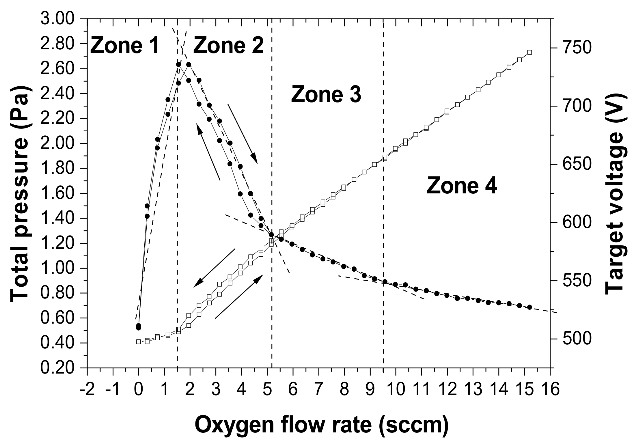
3.1. Reactivity of O2 with Respect to W Target

Before the deposition of the WOx thin films, we first studied the reactivity of O2 with W for a constant argon pressure of 0.41 Pa. Therefore, the O2 injected into the deposition chamber reacted mainly with the W target, W sputtered atoms flux and all metals inside the deposition chamber. To assess the reactivity of O2 with respect to the W target in the W–Ar–O2 system, the total pressure in the deposition chamber and the W target voltage were measured systematically for the different O2 flow rates that were introduced into the deposition chamber. To do this, the O2 flow rate was gradually injected from 0 to 15.2 sccm and then reduced back to 0 sccm. For each O2 flow rate that was introduced, the corresponding total pressure and target voltage were recorded, as shown in Figure 1.
According to the total pressure and the target voltage evolution as a function of the O2 flow rate introduced into the deposition reactor, four zones of O2 reactivity with respect to the W target were identified and are presented in Figure 1. The limits between these different zones were indicative and more precisions about these zones are provided at the end of our study in Section 4, considering the characterization results for all WOx films in this study.
  • Zone 1: 0   sccm Q O 2 1.55   sccm
In Zone 1, a small variation in the total pressure evolved from 0.41 to 0.49 Pa for Q (O2) = 0 sccm and Q (O2) = 1.55 sccm, respectively. Contrary to the total pressure, the W target voltage increased abruptly from 509 to about 720 V for Q (O2) = 0 sccm and Q (O2) = 1.55 sccm, respectively. A low O2 flow rate value was sufficient for the target voltage value to increase by almost 200 V between Q (O2) = 0 sccm and Q (O2) = 1.55 sccm. It should be noted that, as with the total pressure, the changes in the target voltage values were almost identical when the oxygen flow rate in Zone 1 increased and decreased and no hysteresis loops were observed.
  • Zone 2: 1.55   sccm < Q O 2 < 5.2   sccm
In this zone, the total pressure increased sharply from 0.49 to 1.19 Pa, while the target voltage dropped rapidly from about 720 to 589 V as the oxygen flow rate increased from 1.55 to 5.2 sccm, respectively. When the O2 flow rate in Zone 2 increased or decreased, the total pressure and target voltage values were shifted, thus forming a small hysteresis loop. This hysteresis loop could indicate an area of low instability in the W-Ar-O2 system [24,25].
  • Zone 3: 5.2   sccm < Q O 2 < 9.5   sccm
In this oxygen flow rate interval, no hysteresis loops were observed on the target voltage when the oxygen flow rate increased and then decreased. The target voltage dropped slowly and progressively from 589 to 549 V when Q (O2) increased. On the other hand, the total pressure increased systematically linearly from 1.19 to 1.9 when Q (O2) increased and presented a very slight shift during the decrease in Q (O2), which seemed to indicate the incomplete oxidation of the target.
  • Zone 4: Q (O2) ≥ 9.5 sccm
When Q (O2) ≥ 9.5 sccm, the total pressure and target voltage evolved linearly with the increase in Q (O2). This meant that no hysteresis loops were observed on the total pressure and the target voltage when the oxygen flow rate increased and then decreased and it allowed us to assume that the oxidation of the tungsten target was only completed in Zone 4.
The change in slope in the evolution of the W target voltage as a function of Q (O2) between Zone 3 and Zone 4 reflected a change in the reactivity of O2 with respect to the tungsten target, while this change was not visible in the evolution of the pressure as a function of Q (O2). These results allow us to separate Zone 3 and Zone 4, exhibiting O2 reactivities with respect to the W target that were close but nevertheless slightly different.

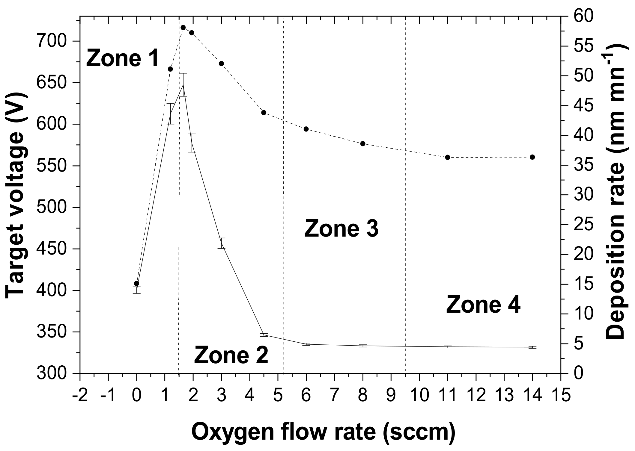
3.2. Synthesis of WOx Films

Several WOx films were synthesized in the previously mentioned four zones for different oxygen flow rates. The oxygen flow rates, total and partial oxygen pressure, target voltage and film thickness values of the synthesized WOx films from this work are summarized in Table 1.
The WOx deposition rate evolution as a function of O2 flow rate ranged from 0 to 14 sccm, as shown in Figure 2, and was similar to the W target voltage evolution. An abrupt increase in the deposition rate from 14 to 48.5 nm·min−1 and in the target voltage from 408 to 716 V was observed for the Q (O2) included in Zone 1. The sudden increase in W target voltage was also observed during the system hysteresis study (Figure 1). Indeed, when the target voltage increased, the Ar+ ions in the plasma became more energetic and were accelerated more toward the tungsten target. Then, the Ar+ ion energies generated an increase in the W sputtering efficiency, which was responsible for the increase in the deposition rate. These poorly oxygen-enriched films were also certainly less dense than the tungsten films and, therefore, thicker after the same deposition time.
In Zone 2, the W target voltage and the deposition rate dropped significantly down to 610 V and 6.4 nm.mn−1, respectively. In Zones 3 and 4, the deposition rate and the W target voltage were very less influenced by the O2 flow rate increase. In Zone 3, the decrease in the deposition rate and the W target voltage were slow and effective, while in Zone 4, the W target voltage continued to slowly decrease due to the increase in total pressure and the deposition rate remained constant at 4.4 nm·min−1.
The decrease in deposition rate and W target voltage from Zone 2 to Zone 4 seemed to be related to the progressive oxidation of the W target and with a gradual change toward the compound sputtering mode. Indeed, the progressive oxidation of the W target caused both a decrease in the sputtering efficiency of the W-O compound formed on the target surface (compared to the W sputtering efficiency) and a decrease in the kinetic energy of the Ar+ ions bombarding the target. The W oxide sputtering efficiency (YWoxide) could be estimated at around 0.15 for Ar+ ions of 500 eV using the equation VdW/VWoxide = YW/YWoxide and knowing the deposition rates of W (Vd W ≈ 15 nm·min−1), tungsten oxide (Vd Woxide ≈ 4.4 nm·min−1) and tungsten sputtering efficiency (YW ≈ 0.5 for Ar+ ions of 500 eV). Several studies have shown that the sputtering efficiency of a ceramic target (oxidized target) is always lower compared to that of a metal target [26,27].
The drop in the deposition rate could also partially be explained by an important decrease in the mean free path of particles removed from the W target and transported under collisions to the substrate when the oxygen flow rate and the total pressure increased in Zones 2 and 3. Our results concerning the evolution of the deposition rate as a function of Q (O2) are comparable to those obtained by Yamamoto et al. [10], with a deposition rate that evolved from 10 to 35 nm·min−1 for low Q (O2) then decreased as the oxygen flow rate increased to reach 2 nm·min−1 when the W target was completely oxidized.

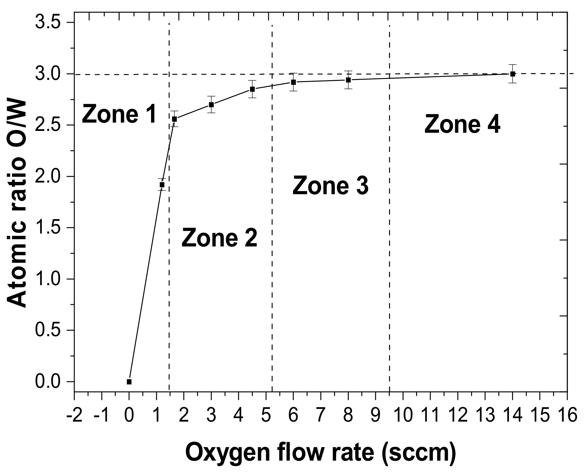
3.3. Chemical Composition

The effect of the oxygen flow rate on the chemical composition of the WOx thin films has been investigated. The chemical composition of the WOx films, as shown in Figure 3, was consistent with results obtained during the hysteresis study (Figure 1), the deposition rate and the target voltage (Figure 2). The evolution of the atomic O-W ratio of the WOx films confirmed the determination of the four zones.
In Zone 1, the high reactivity of tungsten with oxygen was reflected by a rapid enrichment in oxygen for these films. It can be noted that, in Zone 1, the rapid linear increase in the O-W ratio reached the value of 1.92 (close to the stoichiometric WO2 compound with an oxidation state of + 4 for the tungsten atoms). In Zones 2, 3 and 4, the atomic O-W ratio continued to increase more and more slowly to finally reach the value of 3 in Zone 4, which is characteristic of the stochiometric formation of WO3 with an oxidation state of + 6 for the tungsten atoms.
These results show that there was a close link between the parameters of the WOx formation process, such as the hysteresis curves, target voltage, deposition rate and the composition of the deposited films. The choice of oxygen flow rate allowed the deposition of films with variable stoichiometry in terms of oxygen and controllable by the total pressure or the target voltage. The films from Zone 3 were highly oxidized but still sub-stoichiometric, while those from Zone 4 were totally oxidized and stoichiometric, as predicted in Figure 2. The stoichiometric WO3 films were only obtained for oxygen flow rates from around 9.5 sccm and for target voltages close to 560 V. The limit of Q (O2) ≈ 9.5 sccm was assumed at this stage of the study but confirmed by the electrical characterizations, which is discussed in Section 4.
Our results are comparable to those obtained by Parreira et al. [28] (target voltage and chemical composition). In particular, Parreira et al. obtained films with chemical compositions of WO2.92, WO2.86 and WO2.58 for the target voltages of approximately 590, 620, and 678 V, respectively.

3.4. Optical Properties

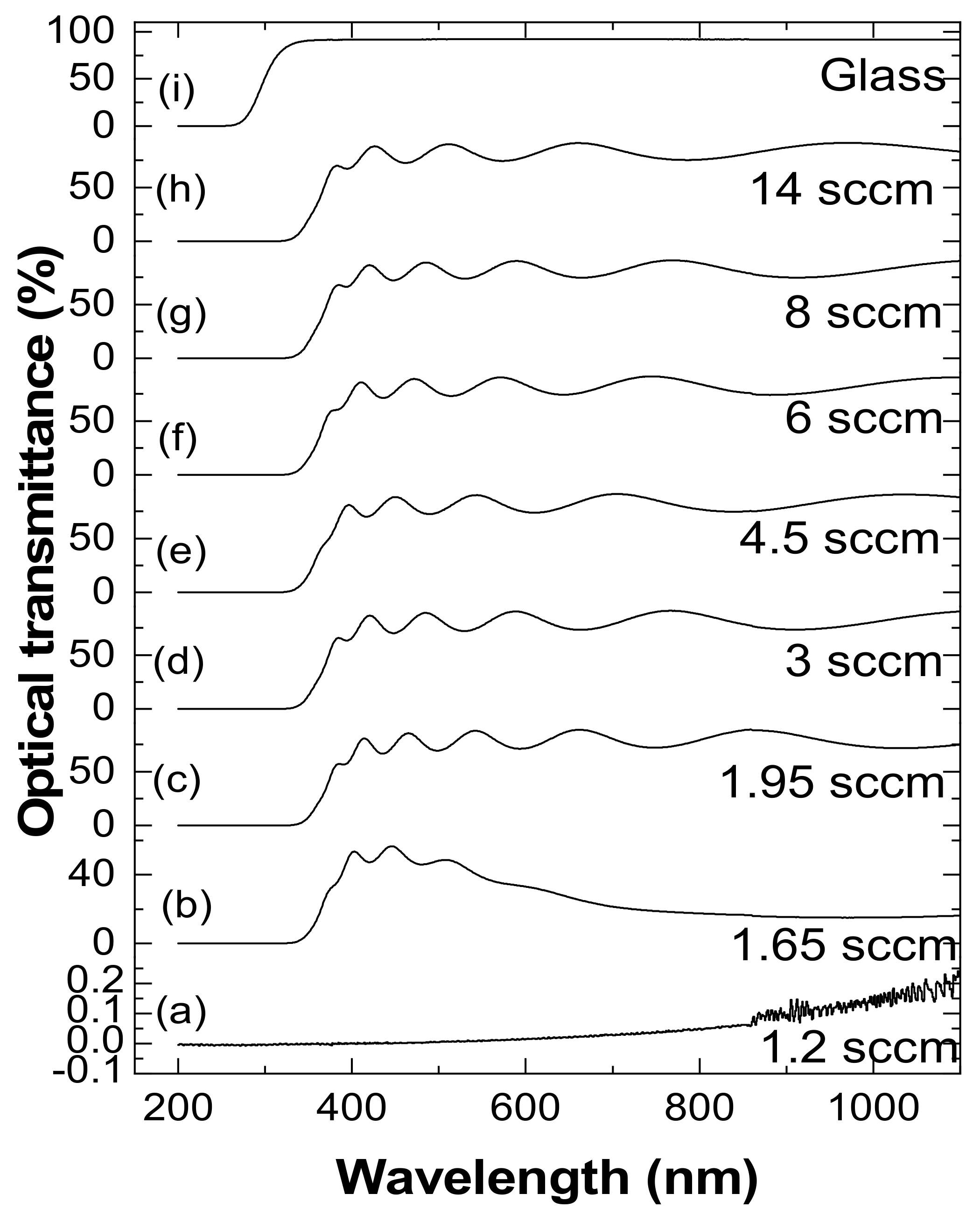
3.4.1. Optical Transmittance

The optical transmittance as a function of the wavelength of different WOx thin films from Zones 1 to 4 is shown in Figure 4 for various oxygen flow rates between 1.2 and 14 sccm. For comparison, glass optical transmittance was also measured (Figure 4i). It was close to 92% in the visible region and its absorption threshold was approximately 260 nm, corresponding to a gap of about 4.8 eV.
The transmittance spectra of the WOx films deposited on glass for flow rates Q (O2) ≥ 1.65 sccm were semi-transparent or transparent, with interference fringes in the visible region and an absorption threshold beyond 310 nm (Figure 4b–h). The absorption threshold for Q (O2) = 1.65 sccm was approximately 325 nm and shifted to 315 nm with the increase in Q (O2) of up to 14 sccm. The strengthening of the W–O covalent bond as Q (O2) increased disfavored inter-atomic electronic transfer and shifted the absorption threshold toward smaller UV wavelengths.
Figure 4 indicates various changes in the optical transmittance of the WOx films from Zone 1 to Zone 4. The film from Zone 1 (Figure 4a) exhibited the lowest optical transmittance in the wavelength range between 400 and 1100 nm. In fact, the film deposited with Q (O2) = 1.2 sccm and chemical formula WO1.92 was totally absorbent and very opaque, with an average transmittance of close to zero in the visible region.
The films in Zones 2 to 4 (Figure 4b–h) evolved from semi-transparent to transparent. The film deposited with Q (O2) = 1.65 sccm and chemical formula WO2.56 had an optical transmittance of between 15% and 55% in the visible region, with the appearance of a few interference fringes. This film presented a pronounced bluish appearance, which is a characteristic of an under-stoichiometric tungsten oxide film: partially transparent and having numerous oxygen vacancies associated to W4+ and W5+, as already observed by Deb et al. [29]. This oxygen sub-stoichiometry favored the absorption of the photon and the electronic transfer between the oxygen valence band and the tungsten conduction band at the origin of the bluing. However, the electronic inter-valence transition between W4+ and W5+ could also give rise to this bluing. The other films had an optical transmittance of between 60% and 88% for the films deposited with Q (O2) = 1.95 sccm and between 65% and 91% for films deposited with Q (O2) = 3 sccm to Q (O2) = 14 sccm in the wavelength range between 400 and 1100 nm. Starting from the flow rate of Q (O2) = 1.95 sccm, the WOx films were totally transparent under our deposition conditions. The increase in Q (O2) beyond 1.95 sccm accentuated the covalent character of the W-O bonds and, therefore, disadvantaged not only the inter-atomic electronic transfer between the O valence band and the W conduction band, but also the electronic inter-valence transition between the less present W4+ and W5+ ions in the transparent films.
Finally, from Figure 4, we can see that the improvement in the optical transmission of the films obtained in Zones 1 to 4 was essentially due to their progressive enrichment in oxygen. All transparent films were found in zones of high oxygen flow rate, i.e., from Q (O2) > 1.65 sccm.

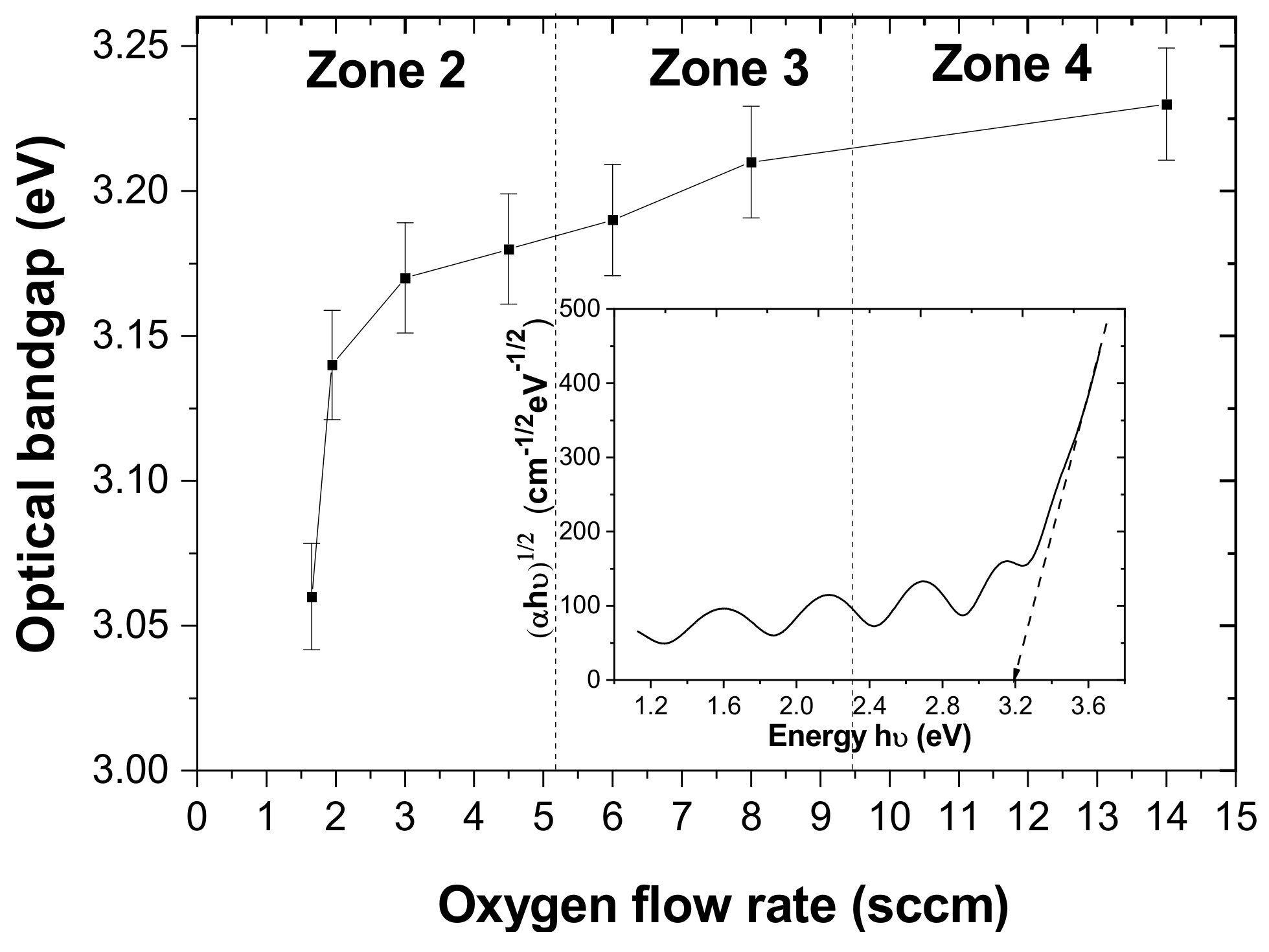
3.4.2. Optical Band Gap

The optical band gap of WOx thin film was determined by the extrapolation of the increasing and linear part of the curve obtained from the Tauc plot method [30], according to the following equation:
α h ϑ 1 n = f h ϑ        
where α is the absorption coefficient and n is a number characterizing the electronic transition process, which can take the values 1/2, 3/2, 2 or 3 depending on whether the transition is direct permitted, direct forbidden, indirect permitted or indirect forbidden, respectively [31]. The research of Hjelm et al. [32] showed that the WO3 compounds have indirect permitted transitions with n = 2. The value of the optical band gap was then obtained by plotting the curve ( α h ν ) 1 / 2 as a function of the energy . The optical band gap evolution as a function of the oxygen flow rate deposited from Q (O2) = 1.65 to 14 sccm is shown in Figure 5.
According to Figure 5, the optical band gap increased from Zones 2 to 4. In fact, the band gap of the WOx films deposited between Q (O2) = 1.65 sccm and Q (O2) = 14 sccm evolved from 3.06 to 3.23 eV, respectively. We can assume that our deposited films were amorphous because these values are consistent with amorphous coating structures [33,34]. In comparison, the optical band gaps of nanocrystallized WO3 films that are reported in the literature are generally between 2.6 and 3 eV [29,35,36].
The increase in the optical band gap with Q (O2) could be due to the enrichment in oxygen of the WOx films. For this reason, Migas et al. [37] showed, by simulation, that the increase in oxygen deficiency in WO3 decreases the optical band gap value.
As soon as Q (O2) increased, the transparent WOx films contained reinforced W-O covalent bonds, which would probably disadvantage the electronic transfers between the oxygen valence band and the tungsten conduction band and cause the increase in the optical band gap. On the other hand, for bluish films that were not completely transparent, the low optical band gap values certainly reflected an improvement in the inter-valence electronic transfer between the W4+ and W5+ cations, which were very present in these films that were poorer in oxygen. The evolution of Figure 5 is similar to that of Figure 3 and confirms our proposed zone classifications.

3.5. Electrical Properties

3.5.1. Electrical Resistivity

The electrical properties of the W-based conductive films deposited with Q (O2) = 0 sccm, 1.2 sccm and 1.65 sccm were determined by conventional resistivity measurements according to the four probe method (see Section 2.2). An increase in electrical resistivity with increasing oxygen flow rate was observed. The measured electrical resistivities were 5.30 × 10⁻⁵, 1.45 × 10⁻², and 25.4 Ω·cm for Q (O2) = 0, 1.2, and 1.65 sccm, respectively. The resistivity value close to 5 × 10⁻⁵ Ω·cm for the film deposited with Q (O2) = 0 sccm was consistent with the value in the literature. Indeed, during their study on electrical resistivity in W thin films that had been sputter deposited by GLAD (glancing angle deposition), Beainoua et al. [38] calculated a resistivity of W equal to 1.3 × 10⁻⁵ Ω·cm at room temperature. We must specify that the electrical resistivity of the tungsten bulk was 5.4 × 10⁻⁶ Ω·cm [39]. The calculated resistivity of the W thin film was always higher than that of the W bulk.
In addition, the introduction of O2 with a low flow rate immediately led to a strong increase in the electrical resistivity, which increased up to 2.54 × 101 Ω·cm for Q (O2) = 1.65 sccm. This strong increase in the electrical resistivity of the films was caused by oxygen enrichment. From the investigations of Xu et al. and Goldfard et al. [13,40], the conductivity of tungsten oxide films is related to the O 2p band relative intensity in the valence band spectral region. The O 2p band grows with oxygen concentration, at the expense of the W d band. As a result, the decrease in conductivity vs. Q (O2) is due to the reverse evolution of the contribution of the O 2p and d bands to the intensity of the valence band region.
The electrical resistivity measurement attributed a conductive behavior to the films deposited with Q (O2) = 0 and 1.2 sccm, and a semi-conductive behavior to the film deposited with Q (O2) = 1.65 sccm. These electrical properties were consistent with the literature and could be correlated to the optical and chemical composition results. Indeed, according to the literature [41], it has been observed that the deposited WO3−z thin films exhibit different coloration aspects for the different levels of oxygen deficiency: z > 0.5 films are metallic (absorbent) and conductive; z = 0.3–0.5 films are blue and conductive; and z < 0.3 films are transparent and resistive. These findings are independent from the film preparation technique.
Above Q (O2) = 1.65 sccm, the electrical properties of the films were no longer accessible with our four probe device and required the achievement of an MOS structure, where the WOx film constituted the oxide material in the structure.

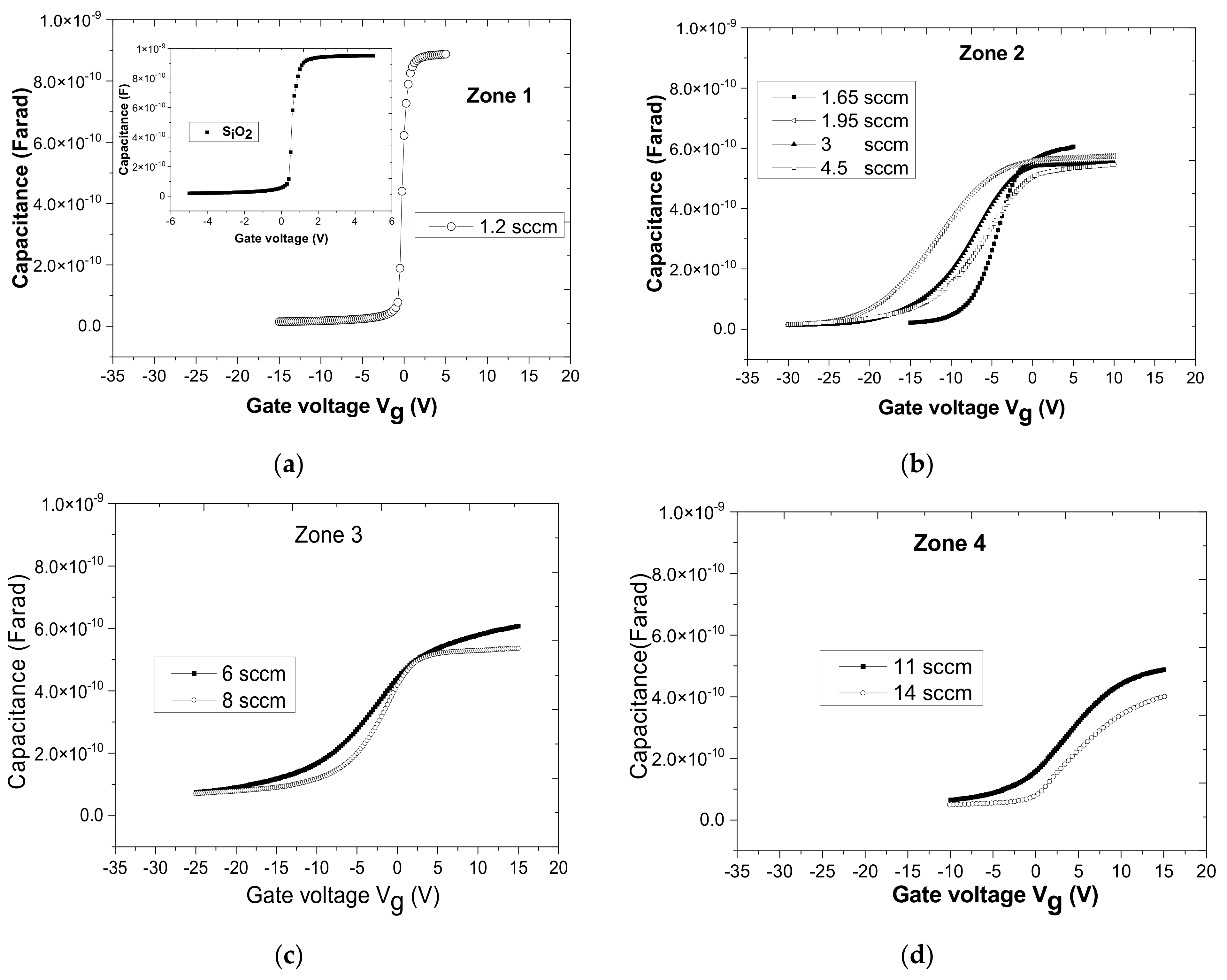
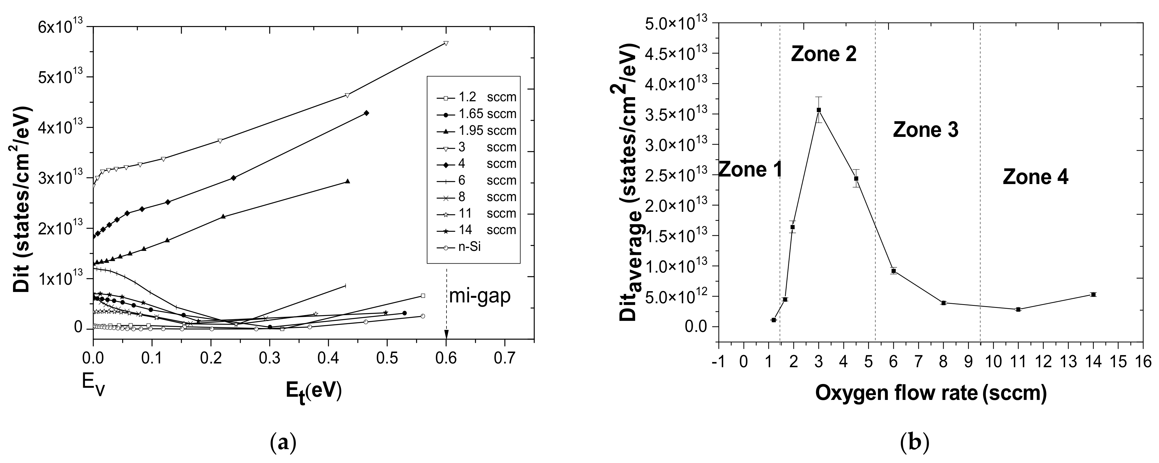
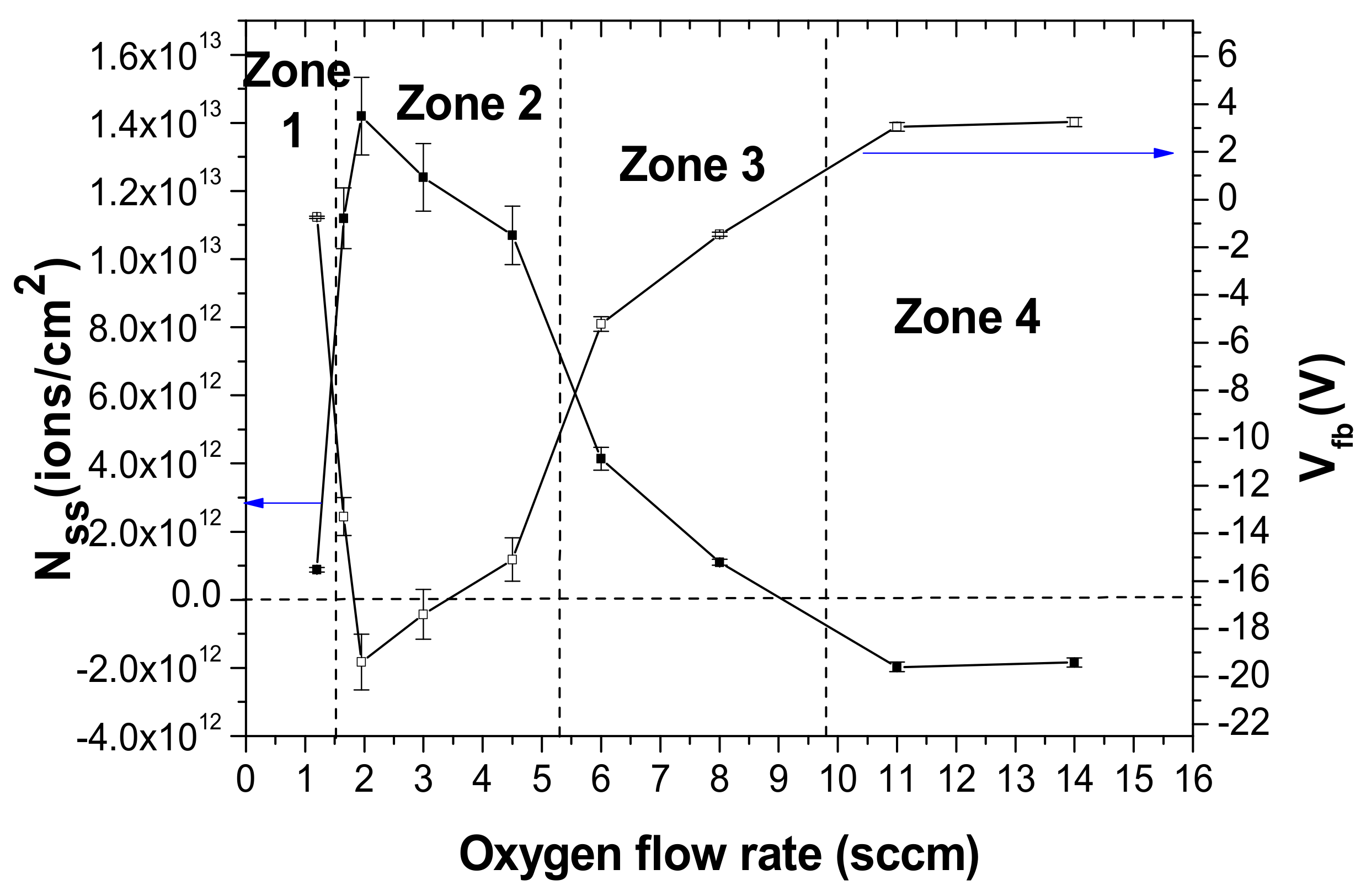
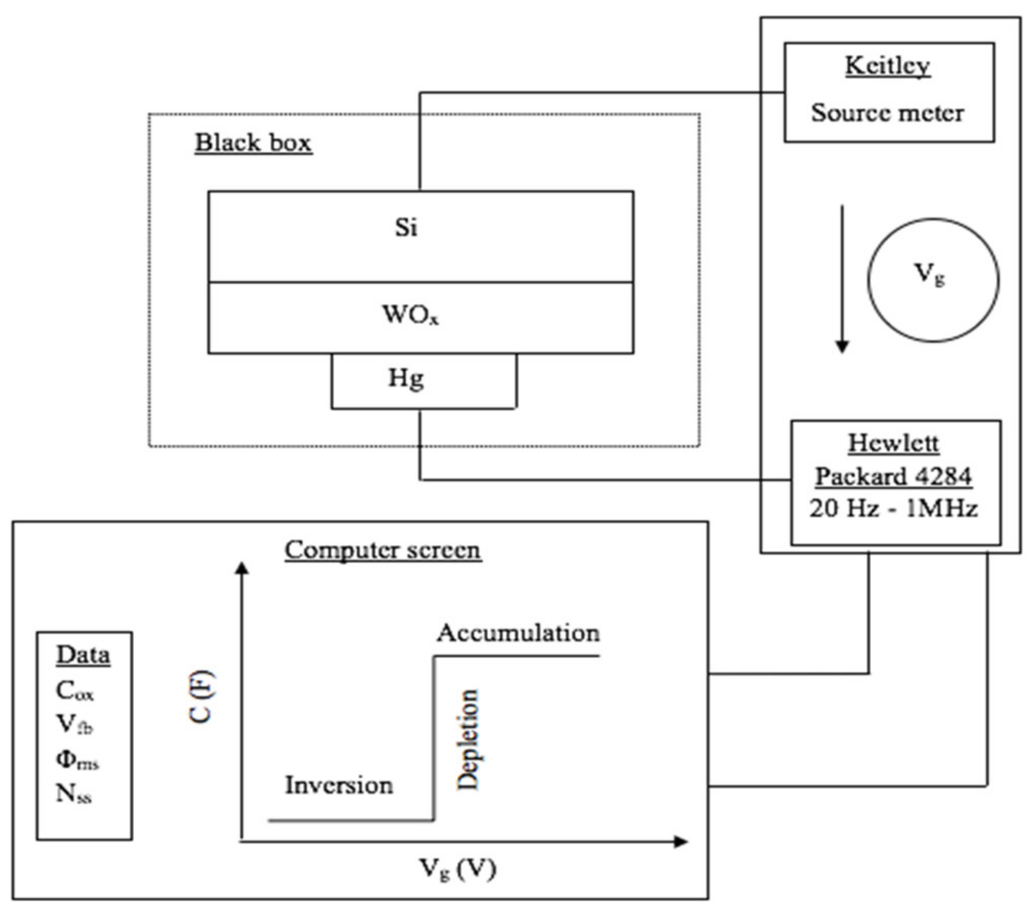
3.5.2. MOS Structures

Figure 6a–d shows the C–V characteristics curves at 1 MHz of Hg-WOx-Si MOS structures. The C-V characteristic curve at 1 MHz of the Hg-SiO2-Si MOS structure was inserted into Figure 6a as a reference. Figure 7a,b represent the effect of oxygen flow rate on the Dit with respect to the energy variation in the silicon band gap and the average density distribution of the interface trap (Dit-average) with respect to the oxygen flow rate at the WOx–Si interface, respectively. Dit was determined using the Terman method [19]. To calculate Dit-average for a given value of Q (O2), we refer to Figure 7a. We summed up each value taken by Dit vs. Et and divided by the total number of Dit vs. Et along the Si band gap.
All C-V characteristics curves at 1 MHz of the MOS capacitance (Figure 6a–d) had three characteristic regions. From the left to the right, we can see the regions of inversion, depletion and accumulation. As the silicon was n-doped, the majority charge carriers were electrons. Indeed, in the region of accumulation with Vg > Vfb, an accumulation of electrons occurred at the WOx–Si interface by electrostatic influence. The depletion region was delimited by Vt < Vg < Vfb, where Vt is the threshold voltage. Finally, the inversion region was reached when Vg < Vt. In this region, all electrons were completely repelled from the WOx–Si interface toward the silicon’s volume by electrostatic influence in order to achieve an inversion layer, which normally contains only positive charges (holes).
The silica (SiO2) was a native oxide layer, which was spontaneously formed on the Si surface. We did not perform any particular treatment other than cleaning the samples with alcohol and our deposits were made on this interfacial SiO2 native oxide layer with a thickness of a few manometers (2–5 nm) [18]. This thickness was negligible compared to the thickness of the WOx thin films (~200 nm). For this reason, although there was a contribution of the SiO2 native oxide layer, this contribution was the same for all samples and, therefore, we could assume that the electrical properties results were mostly dependent on the WOx thin films.
Figure 6a (see insert) shows a sharp transition from the depletion regime (middle) to the accumulation regime (right) of the reference structure Hg–SiO2–Si. This sudden variation reflected the excellent quality of the SiO2–Si interface, which contained fewer interface traps [42]. For this reason, Figure 7a (n–Si symbol: ◦) shows that the reference structure had the lowest interface trap density distribution. The measured average density distribution for the interface traps of the reference structure was estimated to be 4.08 ± 0.32 × 10¹¹ states/cm2/eV.
A change in the shape of the C–V characteristics curves at 1 MHz for all Hg–WOx–Si structures compared to the reference structure can be observed in Figure 6a–d. In Zone 1 (Figure 6a), the MOS structure obtained with Q (O2) = 1.2 sccm and chemical formula WO1.92 had a C-V characteristic curve similar to that of the reference Hg-SiO2-Si structure. Its transition from depletion to accumulation was abrupt. This MOS structure showed the lowest interface trap density distribution (Figure 7a, 1.2 sccm symbol: ▫) because it was close to stoichiometric WO2. The average density of interface traps in this structure (Q (O2) = 1.2 sccm) was estimated to be 1.13 ± 0.09 × 10¹² states/cm2/eV (Figure 7b).
In Zone 2 (Figure 6b), the C-V characteristics curves of the MOS structures obtained for the films deposited with Q (O2) = 1.65, 1.95, 3, and 4.5 sccm tended to flatten in the depletion regime compared to the reference C-V curve. This phenomenon reflected the effects occurring at the oxide–semiconductor interface and indicated the beginning of the degradation of the interface quality. Figure 7a shows that the interface trap density distribution at the WOx-Si interface of the MOS structures for the WOx films in Zone 2 (1.55 sccm < Q (O2) < 5.2 sccm) increased significantly to reach a maximum Dit with Q (O2) = 3 sccm, then decreased again for Q (O2) = 4.5 sccm. It also presents the maximum for the MOS structure obtained with Q (O2) = 3 sccm and chemical formula WO2.70 and an interface trap average density of 3.57 ± 0.28 × 10¹³ states/cm2/eV (Figure 7b). The structural and/or lattice disagreement between these oxides and Si or their non-stoichiometry, which are the main causes of interface states, might be more important for these oxide films in Zone 2, for which the atomic O-W ratio was far from two (WO2) or three (WO3) (Figure 3).
Zones 3 and 4 (Figure 6c,d), for which Q (O2) varied from 6 sccm to 14 sccm, did not show an abrupt transition from the depletion regime to the accumulation regime either. This also indicated the presence of traps at the WOx–Si interface in these structures. Nevertheless, according to Figure 7a, we can observe a fall in the interface trap density distribution in these zones. In Zone 3, with Q (O2) = 6 and 8 sccm and chemical compositions WO2.92 and WO2.94, the interface trap average density decreased from 9.22 ± 0.74 × 10¹² to 3.95 ± 0.28 × 10¹² states/cm2/eV, respectively (Figure 7b). This occurred as the number of interface traps decreased, which was when we tended toward the WO3 stoichiometry. In Zone 4, the interface trap density became significantly lower for the MOS structure obtained for Q (O2) = 11 sccm with an interface trap average density equal to 2.86 ± 0.22 × 10¹² states/cm2/eV (Figure 7b). The slight increase in the interface trap average density for the MOS structure obtained with Q (O2) = 14 sccm, which was equal to 5.31 ± 0.42 × 10¹² states/cm2/eV (Figure 7b), could reflect the presence of oxygen atoms in the interstitials site of this oxide. Finally, according to Figure 7a, all interface trap density distributions were located in the lower part of the silicon band gap. As a result, we can say that interface states are of the donor-type [43].
A drop in the oxide capacitance (Cox) was observed as we evolved from Zone 1 (900 pF) to Zone 4 (400 pF) (Figure 6a–d). This could be related to the resistive nature of the WOx films deposited with a higher oxygen flow rate [44] and also linked to the covalent strengthening of W-O bonds when Q (O2) increases. In Figure 6a–d, it is also important to note the different gate voltage ranges for the different zones. The choice of the gate voltage interval had to be imperatively adapted to each oxide and beyond this interval, the WOx films could become damaged.
The effect of oxygen flow rate on the Nss and the Vfb evolution is shown in Figure 8. This figure shows the evolution of Nss and Vfb as a function of the oxygen flow rate. We can easily notice that these variations were opposite and different from one zone to another. The question that arises concerns the nature and the degree of the oxidation of these ions. In fact, tungsten trioxide (WO3) has a cubic perovskite-like structure that is based on a corner-sharing WO6 octahedra [45]. When deposited at room temperature, WO3 is a monoclinic octahedron with W at the center surrounded by six neighboring oxygen molecules, whereas WO2 can be considered as a quadrilateral with a central W and four neighboring oxygen molecules [46]. Based on the literature [41,46], the most common valence states of W in as-deposited WO3 are W6+ and W4+ in strongly oxygen-deficient material, but in less oxygen-deficient material, both W4+, W5+ and W6+ may be formed. Generally, W5+ is formed by the electrochemical reduction of W6+ [45,47]. Therefore, the formation of a W5+ valence state in as-deposited WO3 films is unlikely, but not impossible. The W5+ valence state can be viewed as the consequence of incomplete bonding between W and O in the octahedron [41,48].
On the other hand, considering the oxygen vacancies in the films and the valence states of tungsten and oxygen, the Nss shown in Figure 8 could reflect the evolution of charged species with the general formula ( WO 2 z ) ε + 0 ≤ z 2 and ( WO 3 ± z ) ε 0 < z < 1. The ( WO 2 z ) ε + are supposed to be positive species with regard to W4+ and O2- valence states and dangling bonds in the quadrilateral. In stoichiometric films, such as WO2 and WO3, we assume ε = 0 because they are considered as neutral species. In sub-stoichiometric films, with the general formula ( WO 3 z ) ε + and ( WO 2 z ) ε + , ε may be positive (+) because of oxygen vacancies in the films, dangling bonds and the W4+, W5+ and W6+ valence states. Finally, in over-stoichiometric films with the general formula ( WO 3 + z ) ε , ε may be negative (−) because, in these films, there are no more oxygen vacancies and the excess oxygen molecules are placed into interstitial sites.
A close link between the evolution of Nss and the evolution of C-V curves was observed. Indeed, according to Figure 6a,b, in Zones 1 and 2, when the oxygen flow rate increased from Q (O2) = 1.2 sccm to Q (O2) = 1.65 sccm, a shift in the C-V curves and the flat band voltage toward the negative gate voltage was observed. This shift toward the negative gate voltages reflected a progressive increase in the positive charges of the ( WO 2 z ) ε + or ( WO 3 z ) ε + that were present in the oxide [49] from Q (O2) = 1.2 sccm to Q (O2) = 1.65 sccm, as shown in Figure 8. In the film deposited with Q (O2) = 1.2 sccm and atomic O–W ratio of 1.92 ± 0.06, we could probably find a combination of WO2 that were neutral species and a few amounts of ( WO 2 z ) ε + that were positive species because of the W4+ and O2- valence states in the quadrilateral. Nss was close to zero in the film deposited with Q (O2) = 1.2 sccm, perhaps because of an important neutral charge amount (WO2) in this film. The film deposited with Q (O2) = 1.65 sccm in Zone 2 with an atomic O–W ratio of 2.56 ± 0.08 was becoming a little bit transparent because of a possible combination of WO2 and ( WO 3 z ) ε + . The ( WO 3 z ) ε + positive charges might contain W6+ valence states, which are responsible for transparent films.
In Zone 2, the MOS structures obtained with Q (O2) = 1.95, 3, and 4.5 sccm (Figure 6a), which showed the most shifted C-V curves toward the negative gate voltages, presented the lowest flat band voltages (Figure 8). These films, with 2.60 ± 0.08 < atomic O–W ratio < 2.90 ± 0.09, might contain the maximum quantity of positive species ( WO 3 z ) ε + and oxygen vacancies. We may find a combination of W4+ and W6+ valence states in those films. According to Figure 4c–e, these films had an average optical transmission of close to 80% in the visible region, reflecting that positive species ( WO 3 z ) ε + with a W6+ valence state were predominant. From Q (O2) = 6 sccm to Q (O2) = 14 sccm, the C–V curves and flat band voltages shifted progressively from a negative gate voltage to a positive one (Figure 6c,d). This C–V curve evolution reflected the decrease in the number of positive species ( WO 3 z ) ε +   in these oxides [49] due to the fulfilment of oxygen vacancies when Q (O2) increased from Q (O2) = 1.95 sccm. Above Q (O2) = 1.95 sccm, we could find combinations of positive charges, such as ( WO 3 z ) ε + , and neutral charges, such as WO3 and WO2, with W6+, W5+ and W4+ valence states. Since films in these regions presented an average optical transmittance of above 80% in the visible spectral region, we could assume that the tungsten valence states of W6+ were predominant compared to W4+ and W5+.
Figure 8 shows the negative values of Nss and the positive values of Vfb for both films deposited with Q (O2) = 11 sccm and Q (O2) = 14 sccm (Zone 4). The values of Nss and Vfb, which were almost constant, meant that negative charges were predominant in these films [49]. All oxygen vacancies seemed to be fulfilled by oxygen, so we could assume that we could no longer find positive charges ( WO 3 z ) ε + in these films. Indeed, when all oxygen vacancies in the WO6 octahedra or WO3 were fulfilled, the excess oxygen flow rate could generate O2− ions, which could be placed into interstitial sites between the WO6 octahedra in the WO3 films. In this situation, the Nss corresponded to negative species ( WO 3 + z ) ε with W6+ valence states in the octahedra. In Zone 4, the films were stoichiometric or over-stoichiometric, according to results of the atomic O–W ratio (Figure 3).
According to Figure 8, Vfb and Nss evolved inversely with respect to each other. Additionally, the more the flat band voltage shifted toward the positive gate voltages, the fewer positive charges were created in the oxide and the more negative charges were created in the oxide. These observations could be correlated with the composition of the films (Figure 3). Indeed, for an Nss of close to zero or negative, the films appeared close to the stoichiometry, or were stoichiometric or over-stoichiometric. For example, the film obtained with Q (O2) = 1.2 sccm presented an Nss of close to zero with an atomic O–W ratio of within 1.92 ± 0.06 of WO2. Contrastingly, the film deposited with Q (O2) = 14 sccm and the atomic O-W ratio of within 3 ± 0.09 of WO3 presented a negative value of Nss. On the other hand, as soon as the Nss increased, the atomic O-W ratio moved away from the stoichiometry of both WO2 and WO3.

4. Description of the Formation of the Different WOx Film Zones

Based on the different trends observed on the W target voltage during the study of the W–Ar–O2 system hysteresis (Figure 1), the chemical composition and the optical and electrical properties, we classified the WOx film formation process into four zones, in contrast to the literature, which proposes three zones [10,12,13]. The W–Ar–O2 system hysteresis was not studied by the authors who suggested three zones for the WOx formation process. However, in agreement with these authors, we determined the same extreme zones: namely, Zone 1 and Zone 4 in our study. The WOx deposition rate evolution in this study was also similar to that in the study of Yamamoto et al. [10].
In the zone 1, delimited by, 0   sccm Q O 2 1.55   sccm , the W target was globally kept in the metallic state (metal target mode) despite the small amount of O2 that was introduced into the deposition chamber. Indeed, the O2 molecules injected into the deposition chamber were trapped by the getter effect on the deposition chamber walls that were receiving the tungsten, the polarized tungsten target and the sputtered tungsten atoms [10]. Due to this getter effect, a very weak variation in total pressure or partial O2 pressure was observed during the increase and decrease in Q (O2) in this region. This weak variation in oxygen pressure was also observed by Mohamed et al. [12]. In this metal target mode, the deposition rate and the target voltage increased abruptly. This sudden increase in W target voltage for lower O2 flow rates was also observed by Sadiki et al. [50]. For Yamamoto et al. [10], films formed in this region of a metal target mode are W or W3O, with an appearance of WO2 in films deposited at 500 °C. They were absorbent and electrically conductive. For Mohamed et al. [12], absorbent WOx (0 < x < 1.5) films were formed but they did not synthesize films above WO1.5 in this region. Regarding these results, we can say that our results are in accordance with these authors because we formed reflective or absorbent and conductive films for W and WO1.92 with Q (O2) = 0 and 1.2 sccm, respectively.
The WOx films sputter deposited in the high O2 flow rate of Zone 4 ( Q O 2   9.5   sccm ) presented the lowest and most constant deposition rate (4.4 nm·min−1) and W target voltage (560 V). This result reflects that the W target surface was totally coated with an oxide layer, i.e., totally polluted or oxidized. According to Yamamoto et al. [10], the W target is in an oxide target mode. For us, and according to our atomic O–W ratio and Nss results, only stoichiometric WO3 or over-stoichiometric WO3+z (z ≥ 0) was formed in this oxide target mode. All WOx films that were synthesized in this region were transparent and electrically resistive, as we observed in our work.
Between the metal target mode (Zone 1) and the oxide target mode (Zone 4), we found a transition zone (zt). From this transition zone, the O2 introduced into the deposition chamber exceeded the getter effect observed in Zone 1. This transition zone has not been clearly discussed in the literature. Indeed, Mohamed et al. [12] did not perform any samples in this region during their study, contrary to Yamamoto et al. [10] and Xu et al. [13]. Mohamed et al. [12] also performed their study with a constant total pressure of 1.2 Pa and Yamamoto et al. [10] performed theirs with 5 mtorr (0.66 Pa). Xu et al. [13] synthesized WOx films by periodically pulsing the O2 flow rate in order to avalanche the reactive sputtering process between the metal target mode and the oxide target mode. As far as we are concerned, we synthesized the WOx films by varying the total pressure through the variation in the oxygen flow rate. Therefore, our total pressure varied from 0.4 to 1.8 Pa in this transition zone. For Yamamoto et al. [10], the W target was still kept in a metallic state (metal target mode) and the WOx ( 2 x < 3 ) films were formed by the reaction of W and O atoms on the surface of the substrate, with the amount of O2 molecules exceeding the getter effect. Unfortunately, their results are not supported by any chemical analysis measurements in this zone. For Yamamoto et al. [10] and Xu et al. [13], these WOx ( 2 x < 3 ) films were also semi-transparent and resistive or semi-conducting. In our study, during the formation of WOx ( 2.56 x 2.94 ) in the transition zone corresponding to 1.65 Q (O2) 8 sccm, we observed a decay in the deposition rate, as observed by Yamamoto et al. [10], and a decay in the target voltage. This decay meant that the W target was no longer kept in its metallic state, as assumed by Yamamoto et al. [10], but it actually started oxidizing.
In addition, in this transition zone, we observed that the optical transmittance and the electrical properties of the film evolved from semi-transparent (%T < 50) and semi-conducting (for WO2.56, Q (O2) = 1.65 sccm) to transparent (between 70% to 90% in the visible region) and resistive (for other films). By only considering these optical transmittance results as a function of the wavelength, we could assume that this transition zone beyond 1.65 sccm produces films with identical behaviors. However, several observations led us to believe that these films were not all identical. Indeed, films prepared for 1.65 sccm < Q (O2) ≤ 4.5 sccm had similar but different behaviors from films prepared with 6 ≤ Q (O2) ≤ 8 sccm. The formation process, chemical composition and electrical properties are good indicators to observe these similar and different behaviors of the films. For this reason, we proposed the subdivision of this transition zone of WOx (2 ≤ x < 3) into two distinct zones, i.e., Zone 2 for 1.55 sccm < Q (O2) < 5.2 sccm and Zone 3 for 5.2 sccm < Q (O2) < 9.5 sccm. Zone 3 constituted the end of the transition zone. That justified the small variations observed in the data and in the trends that were proposed, in particular in the chemical composition, deposition rate, target voltage, etc. of the films in Zones 3 and 4.

5. Conclusions

In this work, WOx thin films were synthesized using the DC reactive magnetron sputtering method. Based on links observed between the W-Ar-O2 system hysteresis, deposition rate, target voltage, chemical composition and electrical properties, we proposed four zones of WOx film formation with different stoichiometries. Each zone was delimited by different oxygen flow rates.
In Zone 1, 0 < Q (O2) 1.55 sccm and the deposition rate and the target voltage increased rapidly when the oxygen flow rate increased. In Zone 1, the films were progressively opaque and bluish with the increase in Q (O2). They presented the lowest values of optical band gap and were electrically conductive. Positive charges associated with oxygen vacancies were progressively created in these films when the oxygen flow rate increased. The film deposited with Q (O2) = 1.2 sccm and close to stoichiometric WO2 presented the lowest interface trap distribution, reflecting the good quality of the WO2–Si interface.
For 1.55 sccm < Q (O2) < 9.5 sccm and Q (O2) 9.5 sccm, the deposition rate and target voltage decreased when Q (O2) increased from 1.95 sccm to 14 sccm. These films were all transparent and their optical band gap increased with Q (O2). Above Q (O2) = 1.95 sccm, a decrease in the positive charges created in these films was observed. When all oxygen vacancies were fulfilled, a further increase in oxygen flow rate introduced into the deposition chamber favored the creation of negative charges in the films, as observed when Q (O2) 9.5 sccm. According to the results of the chemical composition, we can conclude that films with negative Nss are stoichiometric or over-stoichiometric.
Finally, films deposited with 1.55 < Q (O2) < 5.2 sccm presented a significant degradation of the WOx–Si interface quality with high Dit values. Nevertheless, the WOx–Si interface quality was improved for films that were close to stoichiometric WO3 and deposited with 5.2 sccm < Q (O2) < 9.5 sccm and Q (O2) 9.5 sccm. As a consequence, we can say that stoichiometric films, WO2 and WO3, are good candidates to create MOS structures with good quality interfaces.

Author Contributions

Conceptualization, C.R. and M.G.; methodology, C.R. and K.B.J-I.N.; formal analysis, C.R. and K.B.J-I.N.; investigation, K.B.J-I.N. and C.R.; resources, C.R., W.H. and Y.M.; writing—review and editing, C.R. and K.B.J-I.N.; visualization, K.B.J-I.N. and C.R.; supervision, C.R.; project administration, C.R.; funding acquisition, C.R. and M.G. All authors have read and agreed to the published version of the manuscript.

Funding

This work was supported by the PMA (Pays Montbéliard Agglomération) and the state of Côte d’Ivoire.

Institutional Review Board Statement

Not applicable.

Informed Consent Statement

Not applicable.

Data Availability Statement

All data were presented in this manuscript.

Conflicts of Interest

The authors declare no conflict of interest.

References

  1. Kaneko, H.; Nagao, F.; Miyake, K. Preparation and properties of the dc reactively sputtered tungsten oxide films. J. Appl. Phys. 1988, 63, 510–517. [Google Scholar] [CrossRef]
  2. Granqvist, C.G. Oxide electrochromics: Why, how, and whither. Sol. Energy Mater. Sol. Cells 2008, 92, 203–208. [Google Scholar] [CrossRef]
  3. Goodarzi, M.T.; Ranjbar, M. Atmospheric flame vapor deposition of WO3 thin films for hydrogen detection with enhanced sensing characteristics. Ceram. Int. 2020, 46, 21248–21255. [Google Scholar] [CrossRef]
  4. Baucke, F.G.K. Electrochromic mirrors with variable reflectance. Sol. Energy Mater. 1987, 16, 67–77. [Google Scholar] [CrossRef]
  5. Granqvist, C.G.; Azens, A.; Heszler, P.; Kish, L.B.; Österlund, L. Nanomaterials for benign indoor environments: Electrochromics for “smart windows”, sensors for air quality, and photo-catalysts for air cleaning. Sol. Energy Mater. Sol. Cells 2007, 91, 355–365. [Google Scholar] [CrossRef]
  6. Tutov, E. MOS structures with amorphous tungsten trioxide for capacitive humidity sensors. Semiconductors 2008, 42, 1561–1563. [Google Scholar] [CrossRef]
  7. Khojier, K.; Zolghadr, S.; Teimoori, F.; Goudarzi, S. Fabrication and characterization of porous WO3 thin film as a high accuracy cyclohexene sensor. Mater. Sci. Semicond. Process. 2020, 118, 105220. [Google Scholar] [CrossRef]
  8. Leitzke, D.W.; Cholant, C.M.; Landarin, D.M.; Lucio, C.S.; Krüger, L.U.; Gündel, A.; Flores, W.H.; Rodrigues, M.P.; Balboni, R.D.C.; Pawlicka, A.; et al. Electrochemical properties of WO3 sol-gel thin films on indium tin oxide/poly(ethylene terephthalate) substrate. Thin Solid Film. 2019, 683, 8–15. [Google Scholar] [CrossRef]
  9. Quy, V.H.V.; Jo, I.-R.; Kang, S.-H.; Ahn, K.-S. Amorphous-crystalline dual phase WO3 synthesized by pulsed-voltage electrodeposition and its application to electrochromic devices. J. Ind. Eng. Chem. 2021, 94, 264–271. [Google Scholar] [CrossRef]
  10. Yamamoto, A.; Abe, Y.; Kawamura, M.; Sasaki, K. Effects of oxygen gettering and target mode change in the formation process of reactively RF sputtered WO x thin films. Vacuum 2002, 66, 269–273. [Google Scholar] [CrossRef]
  11. Monteiro, A.; Costa, M.F.; Almeida, B.; Teixeira, V.; Gago, J.; Roman, E. Structural and optical characterization of WO3 deposited on glass and ITO. Vacuum 2002, 64, 287–291. [Google Scholar] [CrossRef]
  12. Mohamed, S.H.; Mohamed, H.A.; Abd El Ghani, H.A. Development of structural and optical properties of WOx films upon increasing oxygen partial pressure during reactive sputtering. Phys. B Condens. Matter 2011, 406, 831–835. [Google Scholar] [CrossRef]
  13. Xu, X.; Yazdi, M.A.P.; Salut, R.; Cote, J.-M.; Billard, A.; Martin, N. Structure, composition and electronic transport properties of tungsten oxide thin film sputter-deposited by the reactive gas pulsing process. Mater. Chem. Phys. 2018, 205, 391–400. [Google Scholar] [CrossRef]
  14. Regragui, M.; Jousseaume, V.; Addou, M.; Outzourhit, A.; Bernéde, J.C.; El Idrissi, B. Electrical and optical properties of WO3 thin films. Thin Solid Film. 2001, 397, 238–243. [Google Scholar] [CrossRef]
  15. Li, W.; Sasaki, A.; Oozu, H.; Aoki, K.; Kakushima, K.; Kataoka, Y.; Nishiyama, A.; Sugii, N.; Wakabayashi, H.; Tsutsui, K.; et al. Electron transport mechanism of tungsten trioxide powder thin film studied by investigating effect of annealing on resistivity. Microelectron. Reliab. 2015, 55, 407–410. [Google Scholar] [CrossRef]
  16. Raja, M.; Chandrasekaran, J.; Balaji, M.; Kathirvel, P. Investigation of microstructural, optical and dc electrical properties of spin coated Al:WO3 thin films for n-Al:WO3/p-Si heterojunction diodes. Optik 2017, 145, 169–180. [Google Scholar] [CrossRef]
  17. Xin, Y.; Zhou, H.; Ni, X.; Pan, Y.; Zhang, X.; Zheng, J.; Bao, S.; Jin, P. The optical properties of low infrared transmittance WO3−x nanocrystal thin films prepared by DC magnetron sputtering under different oxygen ratios. RSC Adv. 2015, 5, 57757–57763. [Google Scholar] [CrossRef]
  18. Baltakesmez, A.; Tekmen, S.; Güzeldir, B. Temperature dependent current- and capacitance-voltage characteristics of W/n-Si structures with two-dimensional WS2 and three-dimensional WO3 interfaces deposited by RF sputtering technique. Mater. Sci. Semicond. Process. 2020, 118, 105204. [Google Scholar] [CrossRef]
  19. Liu, C.; Zhang, Y.-M.; Zhang, Y.-M.; Lü, H.-L. Interfacial characteristics of Al/Al2O3/ZnO/n-GaAs MOS capacitor. Chin. Phys. B 2013, 22, 076701. [Google Scholar] [CrossRef]
  20. Terman, L.M. An investigation of surface states at a silicon/silicon oxide interface employing metal-oxide-silicon diodes. Solid-State Electron. 1962, 5, 285–299. [Google Scholar] [CrossRef]
  21. Keithley Instruments, Inc. C-V Characterization of MOS Capacitors Using the Model 4200-SCS Semiconductor Characterization System; Keithley Application Note Number 2896; Keithley Instruments, Inc.: Cleveland, OH, USA, 2007. [Google Scholar]
  22. Schroder, D.K. Semiconductor Material and Device Characterization, 3rd ed.; John Wiley & Sons, Inc.: Hoboken, NJ, USA, 2006. [Google Scholar]
  23. Ridaoui, M. Fabrication et Caractérisation de MOSFET III-V à Faible Bande Interdite et Canal Ultra Mince thèse, N° 42401. Ph.D. Thesis, Université Des Sciences et Technologies de Lille, Lille, France, Université de Sherbrooke, Quebec, Canada, 2017. [Google Scholar]
  24. Gao, F.; Li, G.; Xia, Y. Influence of hysteresis effect on properties of reactively sputtered TiAlSiN films. Appl. Surf. Sci. 2018, 431, 160–164. [Google Scholar] [CrossRef] [Green Version]
  25. Meeuwissen, A.; Bosco, G.B.F.; van der Kolk, E. Optical and structural characterization of Tm2O3, TmN, and TmOxNy thin films grown by direct-current reactive magnetron sputtering. Thin Solid Film. 2021, 717, 138450. [Google Scholar] [CrossRef]
  26. Rossnagel, S.M.; Cuomo, J.J.; Westwood, W.D. Handbook of Plasma Processing Technology; Noyes Publcations: Park Ridge, NJ, USA, 1990. [Google Scholar]
  27. Habib, S.; Rizk, A.; Mousa, I. Physical parameters affecting deposition rates of binary alloys in a magnetron sputtering system. Vacuum 1998, 49, 153–160. [Google Scholar] [CrossRef]
  28. Parreira, N.M.G.; Polcar, T.; Cavaleiro, A. Characterization of W–O coatings deposited by magnetron sputtering with reactive gas pulsing. Surf. Coat. Technol. 2007, 201, 5481–5486. [Google Scholar] [CrossRef]
  29. Deb, S. Opportunities and challenges in science and technology of WO3 for electrochromic and related applications. Sol. Energy Mater. Sol. Cells 2008, 92, 245–258. [Google Scholar] [CrossRef]
  30. Tauc, J.; Grigorovici, R.; Vancu, A. Optical Properties and Electronic Structure of Amorphous Germanium. Phys. Status Solidi B 1966, 15, 627–637. [Google Scholar] [CrossRef]
  31. Koffyberg, F.P.; Dwight, K.; Wold, A. Interband transitions of semiconducting oxides determined from photoelectrolysis spectra. Solid State Commun. 1979, 30, 433–437. [Google Scholar] [CrossRef]
  32. Hjelm, A.; Granqvist, C.G.; Wills, J.M. Electronic structure and optical properties of WO3, LiWO3, NaWO3 and HWO3. Phys. Rev. B 1996, 54, 2436–2445. [Google Scholar] [CrossRef]
  33. De Wijs, G.A.; de Groot, R.A. Structure and electronic properties of amorphous WO3. Phys. Rev. B 1999, 60, 16463–16474. [Google Scholar] [CrossRef] [Green Version]
  34. Nakamura, A.; Yamada, S. Fundamental absorption edge of evaporated amorphous WO3 films. Appl. Phys. 1981, 24, 55–59. [Google Scholar] [CrossRef]
  35. González-Borrero, P.P.; Sato, F.; Medina, A.N.; Baesso, M.L.; Bento, A.C.; Baldissera, G.; Persson, C.; Niklasson, G.A.; Granqvist, C.G.; da Silva, A.F. Optical band-gap determination of nanostructured WO3 film. Appl. Phys. Lett. 2010, 96, 061909. [Google Scholar] [CrossRef]
  36. Rao, K.S.; Kanth, B.R.; Devi, G.S.; Mukhopadhyay, P.K. Structural and optical properties of nanocrystalline WO3 thin films. J. Mater. Sci. Mater. Electron. 2011, 22, 1466. [Google Scholar] [CrossRef]
  37. Migas, D.B.; Shaposhnikov, V.L.; Rodin, V.N.; Borisenko, V.E. Tungsten oxides. I. Effects of oxygen vacancies and doping on electronic and optical properties of different phases of WO3. J. Appl. Phys. 2010, 108, 093713. [Google Scholar] [CrossRef]
  38. El Beainou, R.; Chargui, A.; Pedrosa, P.; Mosset, A.; Euphrasie, S.; Vairac, P.; Martin, N. Electrical resistivity and elastic wave propagation anisotropy in glancing angle deposited tungsten and gold thin films. Appl. Surf. Sci. 2019, 475, 606–614. [Google Scholar] [CrossRef] [Green Version]
  39. Lide, D.R. CRC Handbook of Chemistry and Physics, Internet version 2005; CRC Press: Boca Raton, FL, USA, 2005; Available online: http://www.hbcpnetbase.com (accessed on 18 January 2022).
  40. Goldfarb, I.; Miao, F.; Yang, J.J.; Yi, W.; Strachan, J.P.; Zhang, M.-X.; Pickett, M.D.; Medeiros-Ribeiro, G.; Williams, R.S. Electronic structure and transport measurements of amorphous transition-metal oxides: Observation of Fermi glass behavior. Appl. Phys. A 2012, 107, 1–11. [Google Scholar] [CrossRef]
  41. Chatten, R.; Chadwick, A.V.; Rougier, A.; Lindan, P.J.D. The Oxygen Vacancy in Crystal Phases of WO3. J. Phys. Chem. B 2005, 109, 3146–3156. [Google Scholar] [CrossRef]
  42. Wei, D.; Hossain, T.; Garces, N.Y.; Nepal, N.; Meyer, H.M.; Kirkham, M.J.; Eddy, C.R.; Edgar, J.H. Influence of Atomic Layer Deposition Temperatures on TiO2/n-Si MOS Capacitor. J. Solid State Sci. Technol. 2013, 2, N110–N114. [Google Scholar] [CrossRef] [Green Version]
  43. Knoll, M.; Braunig, D.; Fahrner, W.R. Generation of Oxide Charge and Interface States by Ionizing Radiation and by Tunnel Injection Experiments. IEEE Trans. Nucl. Sci. 1982, 29, 1471–1478. [Google Scholar] [CrossRef]
  44. Gordon, B.J. C-V plotting: Myths and methods. Solid State Technol. 1993, 36, 57–62. [Google Scholar]
  45. Granqvist, C.G. Handbook of Inorganic Electrochromic Materials; Elsevier: Amsterdam, The Netherlands, 1995. [Google Scholar]
  46. Li, C.; Hsieh, J.H.; Hung, M.-T.; Huang, B.Q. Electrochromic study on amorphous tungsten oxide films by sputtering. Thin Solid Film. 2015, 587, 75–82. [Google Scholar] [CrossRef]
  47. Lee, S.-H.; Cheong, H.M.; Tracy, C.E.; Mascarenhas, A.; Czanderna, A.W.; Deb, S.K. Electrochromic coloration efficiency of a-WO3−y thin films as a function of oxygen deficiency. Appl. Phys. Lett. 1999, 75, 1541–1543. [Google Scholar] [CrossRef]
  48. Zhang, J.-G.; Benson, D.K.; Tracy, C.E.; Deb, S.K.; Czanderna, A.W.; Bechinger, C. Chromic Mechanism in Amorphous WO3 Films. J. Electrochem. Soc. 1997, 144, 2022. [Google Scholar] [CrossRef] [Green Version]
  49. Boyer, L.; Fruchier, O.; Notingher, P.; Agnel, S.; Toureille, A.; Rousset, B. Analysis of Data Obtained Using the Thermal-Step Method on a MOS Structure—An Electrostatic Approach. IEEE Trans. Ind. Appl. 2010, 46, 1144–1150. [Google Scholar] [CrossRef]
  50. Sadiki, H.; Pierson, J.F.; Rousselot, C.; Martin, N.; Terwagne, G. Properties and electrochromic performances of reactively sputtered tungsten oxide films with water as reactive gas. Surf. Coat. Technol. 2005, 200, 232–235. [Google Scholar] [CrossRef]
Scheme 1. A schematic diagram of the experimental setup of the capacitance meter with a mercury probe. This device imposed a variable gate voltage on the MOS Hg-WOx-Si structure in order to measure the evolution of the capacitance of the MOS structure in the three regions of inversion, depletion and accumulation. The C-V curve was thus obtained with the Cox, Vfb, ms and Nss parameters. The curve shown in this diagram is considered theoretical or ideal due to the sudden change in capacitance in the depletion region.
Coatings 12 00274 sch001
Figure 1. Hysteresis curves reflecting the total pressure (□) and target voltage (●) evolution as a function of O2 flow rate when Q (O2) increased and then decreased. The absolute errors on total pressure and target voltage were ± 0.01 Pa and ± 4 V, respectively.
Coatings 12 00274 g001
Figure 2. The evolution of the W target voltage (dotted line) and deposition rate (line) during the synthesis of WOx films at different oxygen flow rates from each of the four zones of Q (O2). The absolute error on the target voltage was ±4 V.
Coatings 12 00274 g002
Figure 3. The evolution of the atomic O–W ratio as a function of the O2 flow rate.
Coatings 12 00274 g003
Figure 4. The effect of oxygen flow rate on optical transmittance spectra as a function of the wavelength of the WOx films deposited in Zone 1 (a), Zone 2 (be), Zone 3 (f,g) and Zone 4 (h). Glass optical transmittance as a function of the wavelength is represented in Figure (i) as a reference transmittance spectrum. The absolute error on optical transmittance was ±0.05%.
Coatings 12 00274 g004
Figure 5. The evolution of the optical band gap with respect to the oxygen flow rate of the WOx films deposited from Q (O2) = 1.65 sccm to Q (O2) = 14 sccm. The optical band gap determination using the Tauc plot method for Q (O2) = 8 sccm has been inserted.
Coatings 12 00274 g005
Figure 6. C-V characteristics curves at 1 MHz of Hg-WOx-Si MOS structures obtained for the WOx films deposited with: (a) Q (O2) = 1.2 sccm, the C-V curve of the Hg–SiO2–Si MOS structure is inserted as a reference, (b) Q (O2) = 1.65 sccm to 4.5 sccm, (c) Q (O2) = 6 sccm and 8 sccm, (d) Q (O2) = 11 sccm and 14 sccm. The absolute error on the capacitance measure was ±0.005 pF.
Coatings 12 00274 g006
Figure 7. (a) The influence of oxygen flow rate on Dit evolution as a function of the energy variation in the Si band gap. The relative errors on Dit were evaluated as ± 8%. (b) The evolution of Dit-average as a function of the oxygen flow rate.
Coatings 12 00274 g007
Figure 8. The influence of oxygen flow rate on the simultaneous evolution of the Nss ( ) and Vfb (□) of Hg–WOx–Si MOS structures for all WOx films in Zones 1 to 4.
Coatings 12 00274 g008
Table 1. Constant values for total and partial oxygen pressure and target voltage during the sputtering process for different oxygen flow rates and experimental measurements of the thicknesses achieved after WOx deposition onto glass substrates.
Q O2
(sccm)
Total Pressure
(Pa)
Partial Oxygen Pressure (Pa)Target Voltage
(V)
Film Thickness
(nm)
0.000.410.00408350
1.200.450.04666589
1.650.530.12716582
1.950.610.20710565
2.500.730.32687513
3.000.830.42673507
4.501.130.72613500
6.001.370.96594502
8.001.701.29576528
11.002.101.69560481
14.002.602.19560487
Publisher’s Note: MDPI stays neutral with regard to jurisdictional claims in published maps and institutional affiliations.

