Article

The Damage Threshold of Multilayer Film Induced by Femtosecond and Picosecond Laser Pulses

1
State Key Laboratory of Laser Interaction with Matter, Changchun Institute of Optics, Fine Mechanics and Physics, Chinese Academy of Sciences, Changchun 130033, China
2
University of Chinese Academy of Sciences, Beijing 100049, China
3
Key Laboratory of Electro-Optical Countermeasures Test & Evaluation Technology, Luoyang 471003, China
4
Institute of Atomic and Molecular Physics, Jilin University, Changchun 130012, China
*
Authors to whom correspondence should be addressed.
Coatings 2022, 12(2), 251; https://doi.org/10.3390/coatings12020251
Submission received: 5 January 2022 / Revised: 8 February 2022 / Accepted: 10 February 2022 / Published: 15 February 2022

Abstract

:
Laser-induced damage threshold (LIDT) is an essential factor in measuring the anti-laser damage of optical films. The damage threshold and morphology of the Ta2O5/SiO2 multilayer film prepared by electron beam evaporation were studied by femtosecond (50 fs) and picosecond (30 ps) laser irradiations. The results showed that the LIDT of the film was 1.7 J·cm−2 under the femtosecond laser. The damage morphology developed from surface damage to a clear layered structure, and the outline has become more transparent and regular with an increase in the laser fluence. Under the picosecond laser irradiation, the LIDT of the film was 2.0 J·cm−2. The damage morphology developed from small range to thin film layer separation, and the outline changed from blurry to clear with an increase in laser fluence. Therefore, the LIDT of the film decreased with a decrease in the laser pulse width.

1. Introduction

In high-energy laser systems, there are a large number of optical film components, and the ability of these components to resist laser damage seriously affects the operation of the laser system. With the development of high-energy laser systems, the requirements for the ability of optical film to resist laser damage have become higher. Therefore, the laser-induced damage threshold (LIDT) of the film has become an essential basis for designing laser systems and an essential factor for selecting optical film [1,2,3,4]. As a result, obtaining a high LIDT is a hot issue.
The LIDT of the optical film depends on many factors, such as the intrinsic physical properties of the film, preparation technology, etc. In addition to the above factors, the output parameters of pulsed laser have a significant influence on the LIDT [5,6,7,8]. Therefore, the damage of the optical film is a complex process that is extremely accidental and affected by many factors.
The pulse laser is usually divided into three types: Ultrashort pulse lasers with femtosecond/picosecond pulse width on the order of magnitude; short pulse lasers with nanosecond pulse width on the order of magnitude; and long pulse lasers with microsecond pulse width on the order of magnitude. The research on the damage of these three typical pulse width lasers to optical thin film components is of great significance. These studies can provide a theoretical and experimental basis for the rational use of different laser sources and further explore the application prospects of lasers. For this reason, the laser pulse width is an essential factor that can influence the LIDT of the optical film. Laurence et al. used laser pulses with a wavelength of 1053 nm and a pulse width of 1–60 ps to study the role of defects in laser-induced damage of fused silica and of silica films produced by e-beam and plasma-ion assisted deposition processes [9]. Kozlov et al. investigated the physical mechanism and consequent material modification associated with laser-induced damage of multilayer dielectric high reflectors at 0.6 and 100 ps pulses [10]. Yao et al. investigated the damage thresholds of TiO2 single layers and TiO2/SiO2 high reflectors at different pulse widths, and explored the relationship between film damage mechanism and laser pulse width [11]. Wang et al. investigated the damage thresholds of silicon in millisecond, nanosecond, and picosecond lasers [12]. Zhou et al. studied the damage thresholds of K9 glass and UBK7 glass optical components at different pulse widths, then analyzed the pulse-width dependence of damage threshold [13]. Matsukawa et al. studied the pump-beam-induced optical damage depending on the pulse width in 4-dimethylamino-N′-methyl-4′-stilbazolium tosylate crystal [14]. At present, the damage theory of optical thin films with different pulse widths has been formed.
At present, there are many materials used to prepare optical films, such as TiO2, HfO2, ZrO2, Ta2O5, Nb2O5, SiO2, Al2O3, ZnS, etc. Herein, Ta2O5 and SiO2, as high and low refractive index materials, are the two most commonly used optical film materials in visible and near infrared bands. This is due to the fact that the Ta2O5 film has a low absorption rate, high refractive index, wide spectral transmission range (300–10 μm), high dielectric constant (30–35), chemical stability, thermal stability, and good mechanical properties [15,16,17,18]. The SiO2 film has the characteristics of high hardness, high light transmittance, good wear resistance, strong erosion resistance, good insulation, good thermal stability, and good dielectric properties [19]. Based on the excellent properties of Ta2O5/SiO2 film, many researchers have studied the Ta2O5/SiO2 film. Lv et al. prepared Ta2O5 films of different thicknesses by ion beam sputtering and studied the effect of annealing on the stress of Ta2O5 films [20]. Kumar et al. investigated the LIDT of Ta2O5 and Ta2O5/SiO2 films at 532 and 1064 nm [21]. Aydogdu et al. systematically studied the effect of electric field distribution and heat treatment on laser damage performance of multilayer Ta2O5/SiO2 films deposited on glass substrates by ion beam sputtering [22]. However, the damage threshold and morphology of optical films irradiated by femtosecond and picosecond lasers are still lacking. For this reason, we investigated the damage threshold and damage morphology of Ta2O5/SiO2 multilayer film irradiated by femtosecond and picosecond lasers.
In this paper, the main purpose is to compare the damage of femtosecond and picosecond lasers to the film and discuss the damage mechanism. The LIDT of the Ta2O5/SiO2 multilayer film by electron beam evaporation using fused silica as the substrate under femtosecond and picosecond lasers by one-on-one measurement was investigated. In addition, we observed the damage morphology of multilayer film by microscopy, and then analyzed the pulse-width dependence of the damage threshold. Finally, we discussed the damage mechanism of multilayer film under femtosecond and picosecond lasers.

2. Experimental Details

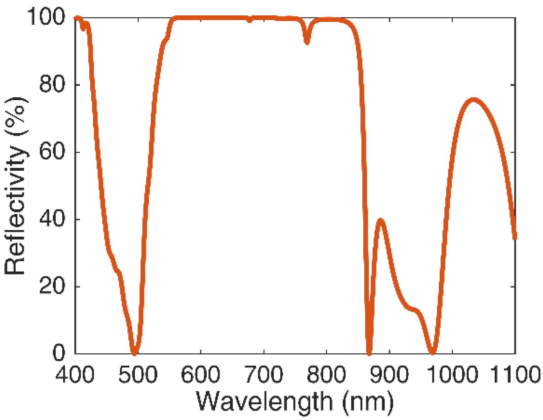
2.1. Sample Customization

To enhance the application of anti-laser damage of thin films in laser systems, suitable all-dielectric multilayer reflective films are often designed according to actual needs. The Ta2O5/SiO2 multilayer film used in the experiment is constructed by electron beam evaporation using fused silica as the substrate. The multilayer film is made of high and low refractive index (Ta2O5 and SiO2) materials with different optical thicknesses. This structure can form a high reflection for a specific band. Figure 1 shows the reflection spectrum curve of the multilayer film, and the spectral range is from 350 to 850 nm.

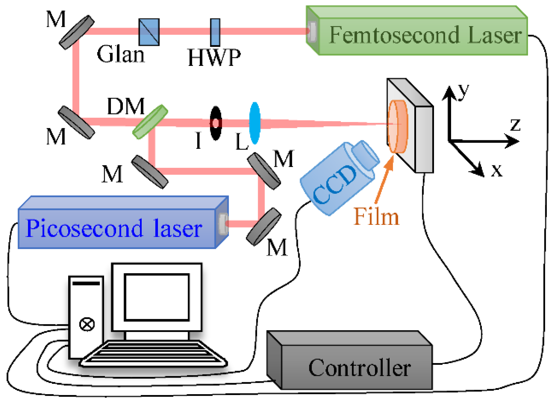
2.2. Experimental Device

Figure 2 shows the experimental setup diagram for the damage of femtosecond and picosecond lasers to the multilayer film. In the experiment, a Ti:sapphire pulse amplification system was used to output a femtosecond laser. Its wavelength and duration were 800 nm and 50 fs, respectively. The wavelength and pulse width of picosecond laser were 1064 nm and 30 ps, respectively. A plane-convex focusing lens (focal length is 25 cm) was used to focus femtosecond and picosecond laser pulses vertically onto the surface of the multilayer film. The spot diameter of femtosecond and picosecond lasers at this position was measured by the blade method as 30 μm. The multilayer film to be tested was fixed on a computer-controlled electric three-dimensional translation stage (PT3/M-Z8, accuracy ±1.5 μm, Thorlabs, Newton, NJ, USA), and the minimum movement step of the translation was 1.0 μm. A microscope and camera were used to observe the experimental process of the damage of femtosecond and picosecond lasers to the multilayer film in real-time. After the experiment, a more sophisticated microscope was used to observe laser damage morphology.

2.3. Laser Damage Threshold Test

The laser damage threshold is a characteristic of calibrating optical films. Since the dielectric film itself absorbs very little laser energy, the various defects have a strong absorption of the laser. The introduction of defects causes the damage of the dielectric film to be random. For the determination of the dielectric film threshold, the experiment used the international standard ISO11254 “1-on-1” mode [23]. During the investigation, the pulse fluence was gradually reduced until the sample was not damaged. Thirty points were sampled at each pulse fluence, and the distance between the two pulse irradiation points on the sample surface was 200 μm. The proportion of damaged test points to all of the test points under each pulse fluence was recorded successively. When the damage probability was zero in the process of reducing the laser fluence, it was the corresponding LIDT [24]. In addition, the ISO 11,254 provides a reference for the LIDT [23]. The file uses a typical nanosecond laser. For the nanosecond pulse width, the main mechanism is defect damage. Under the presupposition, the so-determined damage threshold is only useful under the following conditions:
A.
The mean distance of essential defects is small compared to the spot size.
B.
Most of the defects trigger damage at an identical laser fluence.
Otherwise, the LIDT becomes strongly dependent on the laser spot, and/or the spread becomes very big [23], in which the purpose of the large spot size is to cover enough defects. In the current experiment, the laser spot with 30 μm diameter can cover many defect damage points, in which the mean distance of essential defects is small compared to the spot size (30 μm). For femtosecond laser, the surface damage to the film is intrinsic, in which the defect has almost no effect on the damage of the femtosecond laser. Therefore, a small spot size (30 μm) is reasonable.

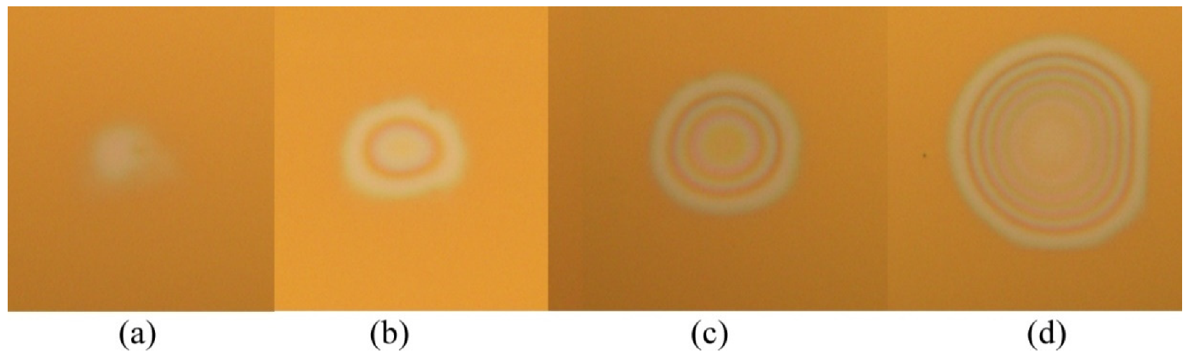
3. Results and Discussion

The difference in damage characteristics or damage mechanism of different pulse width lasers on optical films mainly includes the difference in damage threshold and damage morphology. For this reason, the effect of femtosecond and picosecond lasers on damage threshold and damage morphology of multilayer film was discussed. Figure 3 shows the damage probability distribution of multilayer film irradiated by femtosecond and picosecond lasers. The results show that the LIDTs of the multilayer film are 1.7 and 2.0 J·cm−2 under femtosecond and picosecond lasers. In addition, the LIDT under the picosecond laser is higher than under the femtosecond laser. The LIDT difference between the femtosecond and picosecond lasers is mainly due to the different damage mechanisms. The damage of multilayer films by femtosecond laser can be affected by free electron density and critical energy deposition. When the femtosecond laser radiates the optical film, the absorption of the optical film body causes the ionization of electrons. When the electron density reaches a certain value, the ionizing breakdown damage occurs. However, the damage of picosecond laser to the multilayer film is mainly caused by the thermal effect, which is caused by the absorption of laser energy by defects in the film. To verify this conclusion, a microscope was used to observe the damage morphology of the multilayer film irradiated by femtosecond and picosecond lasers.
Figure 4 and Figure 5 show the damage morphology of the multilayer film irradiated by femtosecond and nanosecond lasers with different laser fluences. There are clear differences in the damage morphology under femtosecond and nanosecond laser irradiations. When the femtosecond laser fluence is near the threshold, the damaged area is a small piece and relatively fuzzy, and there is no discrete damage point at the edge of the damaged area, as shown in Figure 4a. This indicates that the surface damage of the femtosecond laser to the multilayer film is intrinsic, in which the defect has almost no effect on the damage of the femtosecond laser. In addition, the surface damage caused by its nature developed into an evident delamination with an increase in the laser fluence, and the outline was more transparent and regular, as shown in Figure 4b–d. However, when the picosecond laser fluence is near the threshold, the damaged area is not “clean” and “tidy”. Still, it is composed of many tiny damage points, which indicates that there are many minor defects with high absorption of laser energy in the laser-irradiated area, thus causing damage to the film. At this time, the size of damage points is relatively regular and dense, and most of the size is less than 2.0 μm, as shown in Figure 5a. The shallow cracks appear at the edge of the damaged area with an increase in picosecond laser fluence, the outline of the whole damage area is clear, and very dense damage points appear inside the damaged area. At this time, the size of the damaged area is about 15 μm, as shown in Figure 5b. As the picosecond laser fluence continues to increase, the outline of the damaged area becomes clearer and more regular, and there is a trend of surrounding diffusion. The ablation traces of the surface by thermal melting are more clear, and there is a small-scale separation of the film in the center and surrounding edges of the damaged area. At this time, the size of the damaged area is also about 15 μm, as shown in Figure 5c.
The optical thin films have different damage characteristics under femtosecond and picosecond laser irradiations, and the various damage characteristics also reflect different damage mechanisms. A widely accepted view is that when the pulse width is longer than 10.0 ps, the laser’s thermal breakdown of thin films is dominant, and when the pulse width is shorter than 10.0 ps, the optical breakdown of thin films by the laser is dominant [25]. Since the pulse width of the femtosecond laser used in our experiment is 50 fs, the optical breakdown has a dominant effect on the multilayer film. In addition, since the instantaneous peak power of femtosecond laser is very high, the electric field intensity is very high. The nonlinear multiphoton ionization, impact ionization, and tunneling ionization are the primary mechanisms for the damage of the multilayer film. In contrast, the non-intrinsic absorption mechanism caused by impurities and defects is clearly weakened and can be ignored entirely [26]. It is generally believed that nonlinear multiphoton ionization and collision ionization work together when the pulse width of the femtosecond laser is long. When the pulse width is short, multiphoton ionization is enough to damage the film. The main mechanism is the tunneling ionization when the pulse width is very short [27,28]. The pulse width used in our experiment is 50 fs, and thus we only consider the damage effect of multiphoton ionization on the optical film. The initial conduction electrons are generated by multiphoton ionization, and then the conduction electrons rapidly absorb laser energy. When their energy is greater than the bandgap energy of the material, they will collide with valence electrons and generate another electron, thus forming an electron avalanche effect. When its concentration reaches 1021 cm−3, it will cause damage to the thin film [26,28].
However, since the pulse width of the picosecond laser used in our experiment is 30 ps, the thermal breakdown has a dominant effect on the multilayer film. For the picosecond laser, since the intrinsic absorption of multilayer film to the laser is very small, the intrinsic absorption alone is not enough to directly cause the damage of multilayer film. The laser damage to the multilayer film is mainly completed by extrinsic absorption. Therefore, the LIDT of multilayer film depends on the purity of the material or the defects and impurities in the material. The currently recognized defect damage model is the thermal damage model [29]. The defects are regarded as the source of damage, and part of the laser penetrates the defect, which will focus on the inside of the defect to produce an electric field enhancement. The absorption characteristic of the defect itself allows for the laser energy to be absorbed. Since the boundary between the defect and the primary material of the film is discontinuous, the heat flow inside the defect is hindered. A temperature gradient is generated between the defect and the primary material of the film, thereby forming a thermal stress field. When the temperature field and the stress field reach a specific critical value, the mechanical instability of the defect itself makes the position of the defect preferentially undergo thermal damage, thereby causing damage to the film. Therefore, under the current experimental conditions, the damage mechanism of the femtosecond laser to the multilayer film is mainly the ionization effect. In contrast, the damage mechanism of the picosecond laser to the multilayer film is mainly a thermal effect.

4. Conclusions

This paper measured the damage threshold of Ta2O5/SiO2 multilayer film by femtosecond and picosecond lasers. It was found that the LIDTs of multilayer film are 1.7 and 2.0 J·cm−2 under femtosecond and picosecond lasers, respectively. This is due to the fact that the damage mechanism of the femtosecond laser to the multilayer film is mainly the ionization effect. In contrast, the damage mechanism of the picosecond laser to the multilayer film is mainly a thermal effect. In addition, the damage morphology was observed by a microscope. It was found that under femtosecond laser irradiation, the damage caused by its nature develops into an evident delamination with an increase in the laser fluence. The outline was more transparent and regular. However, under picosecond laser irradiation, the point damage caused by the defect developed to the separation of the film layer with an increase in the laser fluence, and the outline changed from blurry to clear.

Author Contributions

Formal analysis, A.C. and L.Z.; Funding acquisition, A.C. and L.Z.; Investigation, X.C., J.S. and C.Z.; Writing–original draft, Y.W.; Writing–review & editing, A.C. All authors have read and agreed to the published version of the manuscript.

Funding

We acknowledge the support by the Fundamental Research Project of Chinese State Key Laboratory of Laser Interaction with Matter (No. SKLLIM1804) and the National Natural Science Foundation of China (Nos. 11674128 and 11974138).

Institutional Review Board Statement

Not applicable.

Informed Consent Statement

Not applicable.

Data Availability Statement

The data presented in this study are available on request from the corresponding author. The data are not publicly available due to the confidentiality.

Conflicts of Interest

The authors declare no conflict of interest.

References

  1. Ghang, Y.; Jin, C.; Li, C.; Deng, W.; Jin, J. ArF excimer laser induced damage on high reflective fluoride film. Laser Technol. 2014, 38, 302–306. [Google Scholar]
  2. Zhu, M.; Yi, K.; Li, D.; Liu, X.; Qi, H.; Shao, J. Influence of SiO2 overcoat layer and electric field distribution on laser damage threshold and damage morphology of transport mirror coatings. Opt. Commun. 2014, 319, 75–79. [Google Scholar] [CrossRef]
  3. Velpula, P.K.; Kramer, D.; Rus, B. Femtosecond laser-induced damage characterization of multilayer dielectric coatings. Coatings 2020, 10, 603. [Google Scholar] [CrossRef]
  4. Yu, H.; Tang, F.; Chen, J.; Yi, Z.; Ye, X.; Wang, Y. Reflective meta-films with anti-damage property via field distribution manipulation. Coatings 2021, 11, 640. [Google Scholar] [CrossRef]
  5. Schaffer, C.B.; Brodeur, A.; Mazur, E. Laser-induced breakdown and damage in bulk transparent materials induced by tightly focused femtosecond laser pulses. Meas. Sci. Technol. 2001, 12, 1784–1794. [Google Scholar] [CrossRef]
  6. Bonod, N.; Néauport, J. Optical performance and laser induced damage threshold improvement of diffraction gratings used as compressors in ultra high intensity lasers. Opt. Commun. 2006, 260, 649–655. [Google Scholar] [CrossRef] [Green Version]
  7. Uteza, O.; Bussière, B.; Canova, F.; Chambaret, J.P.; Delaporte, P.; Itina, T.; Sentis, M. Laser-induced damage threshold of sapphire in nanosecond, picosecond and femtosecond regimes. Appl. Surf. Sci. 2007, 254, 799–803. [Google Scholar] [CrossRef]
  8. Bonse, J.; Solis, J.; Urech, L.; Lippert, T.; Wokaun, A. Femtosecond and nanosecond laser damage thresholds of doped and undoped triazenepolymer thin films. Appl. Surf. Sci. 2007, 253, 7787–7791. [Google Scholar] [CrossRef]
  9. Laurence, T.A.; Negres, R.A.; Ly, S.; Shen, N.; Carr, C.W.; Alessi, D.A.; Rigatti, A.; Bude, J.D. The role of defects in laser-induced modifications of silica coatings and fused silica using picosecond pulses at 1053 nm: II. Scaling laws and the density of precursors. Opt. Express 2017, 25, 15381–15401. [Google Scholar] [CrossRef]
  10. Kozlov, A.A.; Lambropoulos, J.C.; Oliver, J.B.; Hoffman, B.N.; Demos, S.G. Mechanisms of picosecond laser-induced damage in common multilayer dielectric coatings. Sci. Rep. 2019, 9, 607. [Google Scholar] [CrossRef] [Green Version]
  11. Yao, J.; Fan, Z.; Jin, Y.; Zhao, Y.; He, H.; Shao, J. Investigation of damage threshold to TiO2 coatings at different laser wavelength and pulse duration. Thin Solid Film. 2008, 516, 1237–1241. [Google Scholar] [CrossRef]
  12. Wang, X.; Shen, Z.H.; Lu, J.; Ni, X.W. Laser-induced damage threshold of silicon in millisecond, nanosecond, and picosecond regimes. J. Appl. Phys. 2010, 108, 033103. [Google Scholar]
  13. Zhou, X.; Ba, R.; Zheng, Y.; Yuan, J.; Li, W.; Chen, B. The effect of laser pulse width on laser-induced damage at K9 and UBK7 components surface. In Proceedings of the Pacific Rim Laser Damage, Shanghai, China, 17–20 May 2015; Volume 9532. [Google Scholar]
  14. Matsukawa, T.; Nawata, K.; Notake, T.; Qi, F.; Kawamata, H.; Minamide, H. Pump-beam-induced optical damage depended on repetition frequency and pulse width in 4-dimethylamino-n′-methyl-4′-stilbazolium tosylate crystal. Appl. Phys. Lett. 2013, 103, 023302. [Google Scholar] [CrossRef]
  15. Jin-Young, K.; Garg, A.; Rymaszewski, E.J.; Toh-Ming, L. High frequency response of amorphous tantalum oxide thin films. IEEE Trans. Compon. Packag. Technol. 2001, 24, 526–533. [Google Scholar] [CrossRef]
  16. Pecovska-Gjorgjevich, M.; Novkovski, N.; Atanassova, E. Electrical properties of thin rf sputtered Ta2O5 films after constant current stress. Microelectron. Reliab. 2003, 43, 235–241. [Google Scholar] [CrossRef]
  17. Dimitrova, T.; Arshak, K.; Atanassova, E. Crystallization effects in oxygen annealed Ta2O5 thin films on Si. Thin Solid Film. 2001, 381, 31–38. [Google Scholar] [CrossRef]
  18. Shibata, S. Dielectric constants of Ta2O5 thin films deposited by r.F. Sputtering. Thin Solid Film. 1996, 277, 1–4. [Google Scholar] [CrossRef]
  19. Neaton, J.B.; Muller, D.A.; Ashcroft, N.W. Electronic properties of the Si/SiO2 interface from first principles. Phys. Rev. Lett. 2000, 85, 1298–1301. [Google Scholar] [CrossRef]
  20. Lv, Q.; Huang, M.; Zhang, S.; Deng, S.; Gong, F.; Wang, F.; Pan, Y.; Li, G.; Jin, Y. Effects of annealing on residual stress in Ta2O5 films deposited by dual ion beam sputtering. Coatings 2018, 8, 150. [Google Scholar] [CrossRef] [Green Version]
  21. Kumar, S.; Shankar, A.; Kishore, N.; Mukherjee, C.; Kamparath, R.; Thakur, S. Laser induced damage threshold of Ta2O5 and Ta2O5/SiO2 films at 532 and 1064 nm. Optik 2019, 176, 438–447. [Google Scholar] [CrossRef]
  22. Aydogdu, G.H.; Batman, H.; Cosar, M.B.; Ozhan, A.E.S. Enhancement of laser damage resistance at 1064 nm of high and anti-reflective optical multilayers by tailoring the electric field distribution and post-annealing. In Proceedings of the Society of Vacuum Coaters 59th Annual Technical Conference Proceedings, Indianapolis, IN, USA, 9–13 May 2016; pp. 247–251. [Google Scholar]
  23. Becker, J.; Bernhardt, A. ISO 11254: An international standard for the determination of the laser-induced damage threshold. In Proceedings of the SPIE–The International Society for Optical Engineering, Boulder, CO, USA, 27–29 October 1993; Volume 2114, p. 703. [Google Scholar]
  24. Wu, S.J.; Shi, W.; Su, J.H. Using an external electric field to reduce laser damage of dlc films. Int. J. Mater. Prod. Technol. 2013, 45, 74–82. [Google Scholar] [CrossRef]
  25. Du, D.; Liu, X.; Korn, G.; Squier, J.; Mourou, G. Laser-induced breakdown by impact ionization in SiO2 with pulse widths from 7 ns to 150 fs. Appl. Phys. Lett. 1994, 64, 3071. [Google Scholar] [CrossRef] [Green Version]
  26. Jasapara, J.; Nampoothiri, A.V.V.; Rudolph, W.; Ristau, D.; Starke, K. Femtosecond laser pulse induced breakdown in dielectric thin films. Phys. Rev. B 2001, 63, 045117. [Google Scholar] [CrossRef]
  27. Mero, M.; Liu, J.; Rudolph, W.; Ristau, D.; Starke, K. Scaling laws of femtosecond laser pulse induced breakdown in oxide films. Phys. Rev. B 2005, 71, 115109. [Google Scholar] [CrossRef]
  28. Chimier, B.; Utéza, O.; Sanner, N.; Sentis, M.; Itina, T.; Lassonde, P.; Légaré, F.; Vidal, F.; Kieffer, J.C. Damage and ablation thresholds of fused-silica in femtosecond regime. Phys. Rev. B 2011, 84, 094104. [Google Scholar] [CrossRef] [Green Version]
  29. Dijon, J.; Poulingue, M.; Hue, J. Thermomechanical model of mirror laser damage at 1.06 μm: I. Nodule ejection. In Proceedings of the Laser-Induced Damage in Optical Materials: 1998, Boulder, CO, USA, 28 September–1 October 1998; Volume 3578. [Google Scholar]
Figure 1. Reflection spectrum curve of multilayer film.
Coatings 12 00251 g001
Figure 2. Experimental setup for the damage of femtosecond and picosecond lasers to the multilayer film.
Coatings 12 00251 g002
Figure 3. Damage probability distribution of multilayer film irradiated by femtosecond and picosecond lasers with different laser fluences.
Coatings 12 00251 g003
Figure 4. Damage morphology of multilayer film irradiated by femtosecond laser for different fluences. Laser fluences are 1.75 J·cm−2 (a), 1.82 J·cm−2 (b), 1.95 J·cm−2 (c), and 2.26 J·cm−2 (d).
Coatings 12 00251 g004
Figure 5. Damage morphology of multilayer film irradiated by picosecond laser for different fluences. Laser fluences are 2.11 J·cm−2 (a), 2.19 J·cm−2 (b), 2.40 J·cm−2 (c), and 2.71 J·cm−2 (d).
Coatings 12 00251 g005
Publisher’s Note: MDPI stays neutral with regard to jurisdictional claims in published maps and institutional affiliations.

