Article

In Situ Growth of PbS Nanoparticles without Organic Linker on ZnO Nanostructures via Successive Ionic Layer Adsorption and Reaction (SILAR)

1
Electrical Engineering Department, College of Engineering, University of Business and Technology (UBT), Jeddah 21361, Saudi Arabia
2
Sustainable Development, Global Council for Tolerance and Peace, VLT1101 Valetta, Malta
3
Canada Research Chair in Engineered Advanced Materials and Devices, Faculty of Engineering, University of Ottawa, Ottawa, ON K1N 6N5, Canada
4
General Subjects Department, College of Engineering, University of Business and Technology (UBT), Jeddah 21361, Saudi Arabia
5
Faculty of Science, Lebanese University, Tripoli 961, Lebanon
6
Division of Biological and Environmental Sciences and Engineering (BESE), King Abdullah University of Science and Technology (KAUST), Thuwal 23955-6900, Saudi Arabia
7
Institut d’Électronique, de Microélectronique et de Nanotechnologie (IEMN UMR CNRS 8520), Université Polytechnique Hauts de France (UPHF), 59309 Valenciennes, France
*
Author to whom correspondence should be addressed.
Coatings 2022, 12(10), 1486; https://doi.org/10.3390/coatings12101486
Submission received: 8 August 2022 / Revised: 27 September 2022 / Accepted: 3 October 2022 / Published: 6 October 2022

Abstract

:
The process of effective solar energy harvesting and conversion requires efficient photon absorption, followed by charge generation and separation, then electron transfer. Nanostructured materials have been considered as potential building blocks for the development of future generations of solar cells. Much attention has been given to wide-bandgap semiconductor nanowires, combined and sensitized with low-bandgap semiconductors effectively attached to the nanowires for low-cost and highly efficient solar cells. Here, the in situ growth of lead sulfide (PbS) nanoparticles on the surface of zinc oxide (ZnO) nanowires grown by the Successive Ionic Layer Adsorption and Reaction (SILAR) technique is presented for different numbers of cycles. The morphology and structure of PbS nanoparticles are confirmed by Scanning Electron Microscopy (SEM), revealing the decoration of the nanowires with the PbS nanoparticles, Transmission Electron Microscopy (TEM) and HR-TEM, showing the tight attachment of PbS nanoparticles on the surface of the ZnO nanowires. The Selected Area Electron Diffraction (SAED) confirms the crystallization of the PbS. Photoluminescence spectra show a broad and more intense deep-level emission band.

1. Introduction

Zero- and one-dimensional nanostructures [1,2,3,4] have attracted lots of attention due to their unique properties (physical and chemical) in different applications, specifically, in solar energy harvesting [3,5], conversion and storage [6,7,8,9]. Semiconductor NPs, 0D, with their tunable bandgap, span the optical absorption of most of the solar spectrum and have a strong light absorption coefficient compared to Si and organic materials. In addition, NPs provide multiple exciton generation, but are not effective for charge separation and transportation [10], while nanowires (NWs) in solar cells allow charge generation, separation and transportation [11]. The unique geometry of NW arrays allows optical reflection-enhancing light trapping and absorption (Figure 1). They also drive the charge separation and direct the transportation of photo-generated electrons, thus minimizing electron–hole recombination [12].
ZnO NWs have been widely studied over the last decade because of their wide applications in optics, electronics [2,13,14,15,16], clean and sustainable solar cells [17,18,19,20], piezoelectric [21,22,23,24] and sensing [25,26,27,28]. ZnO is a wide-bandgap semiconductor of 3.37 eV and has high exciton energy of 60 meV, which makes it promising for optical devices [29]. The preferred choice of light-absorbing semiconductor nanocrystal is metal chalcogenides (such as PbS, CdS, PbSe, CdSe) [30,31,32] because of their solution processing ability and exhibition of photo-stability in solar cells. The matching of the band energies of the two semiconductors facilitates the desired function to improve the charge separation by driven electrons and holes in two different nanoparticles (Figure 2). PbS has unique properties among other chalcogenides. Its large excitonic Bohr radius (~18 nm) allows the bandgap of PbS particles to be easily tuned anywhere between 0.41 and 2 eV, thus covering the entire visible spectrum [33].
Figure 3 illustrates the hybrid radial junction solar cell where PbS NPs decorate the surface of the ZnO NWs, resulting in a heterojunction interface. This structure reflects a large interface and short carrier diffusion range which will cause efficient carrier separation and transportation and low-charge carrier recombination [34].
PbS colloidal quantum dots (CQDs) are usually synthesized by chemical routes and have an insulating capping layer composed of long hydro-carbon chain such as oleic acid (OA), and thus, in order to improve the charge transport from the QDs to the ZnO NWs, a de-capping process with short ligands such as MPA [35] and EDT [36] is required.
Considering these points, the Chemical Bath Deposition (CBD) and Successive Ionic Layer Adsorption and Reaction (SILAR) methods are advantageous for the direct growth of the PbS NPs. In the CBD method, the PbS NPs’ size can be controlled by changing the reaction time, while in the SILAR method, this can be changed by the number of cycles. The SILAR method is considered a simple and scalable technique [37]. It does not require vacuum nor high temperature, and can be used with different types of substrates, making it promising for industrial applications. SILAR can also pack NPs tightly onto the surface of the ZnO NWs without insulating the nature organic ligand, which affects the electronic structure at the interface and the electron transfer rate [38].
Some researchers have demonstrated PbS-sensitized ZnO nanostructures, but their ZnO NWs were randomly oriented and not very well spaced [19,39,40]. Thus, it is hard to cover the entire ZnO NWs by PbS NPs, and very difficult to deposit the electrode contacts.
Herein, we demonstrate the successful in situ growth of PbS NPs on vertically oriented ZnO NWs using the SILAR technique for different numbers of cycles, without the use of the organic ligand and with full coverage of the nanowires.

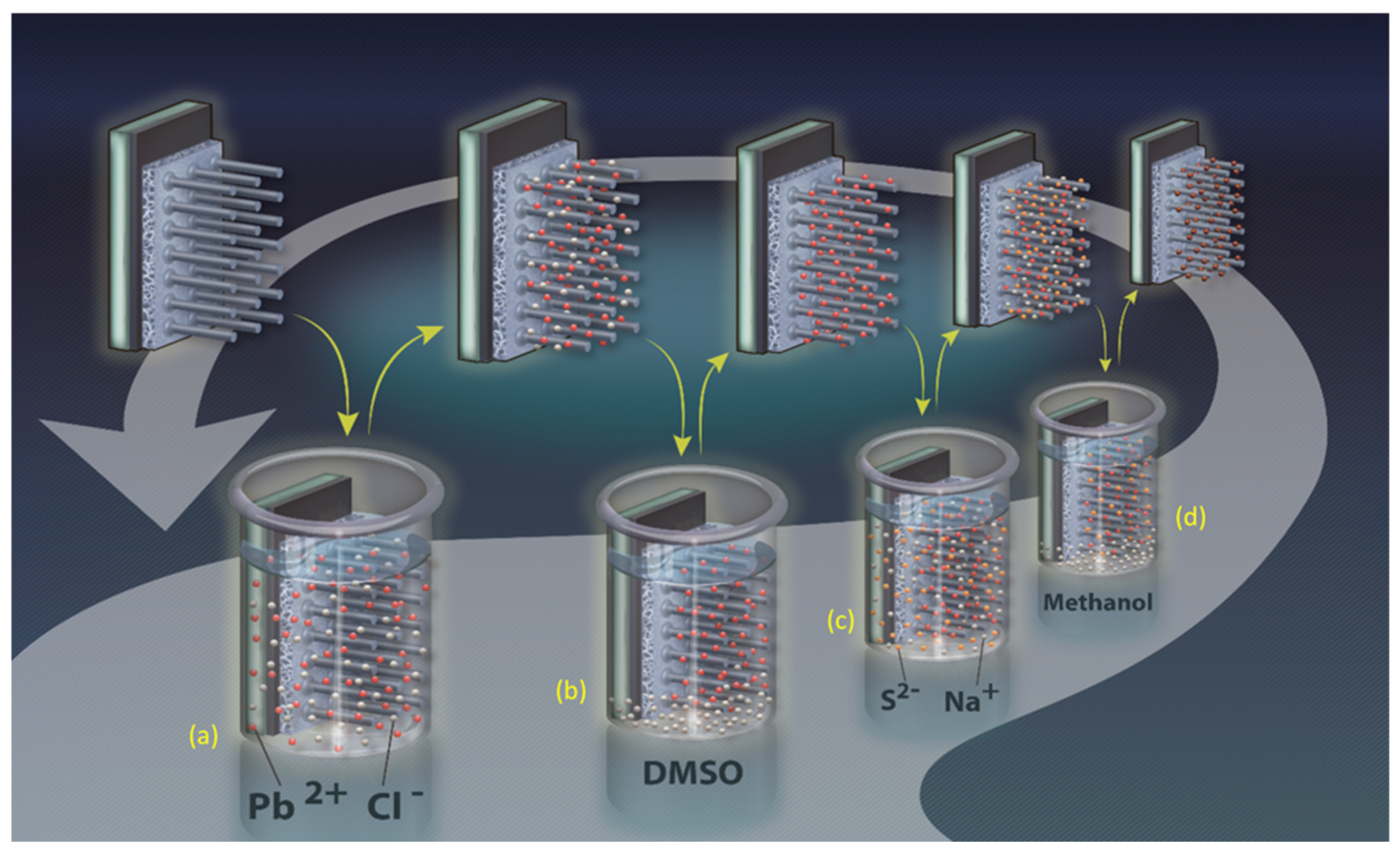
2. Materials and Methods

High-quality vertically oriented NWs were grown perpendicular to the substrate surface by pulsed-laser deposition (PLD) [41] with a length of 1.4 µm, diameter of 50 nm, and spacing of 75 nm. The surface of the free-standing ZnO NWs is hydrophobic; therefore, oxygen plasma ashing was performed for 3 min to make ZnO NWs hydrophilic to obtain better wettability.
PbS nanoparticle growth was carried out at room temperature by a chemical method known as the SILAR method using 2 different solutions: PbCl2 (C1) as a cationic precursor and Na2S (A1) as an anionic precursor. The cationic solution, C1, is composed of 18.4 mg of PbCl2 dissolved in 10 mL methanol PbCl 2 +   CH 4 O Pb 2 + + 2 Cl + , while the anionic solution, A1, is composed of 5.21 mg of Na2S dissolved in 10 mL of dimethyl sulfoxide (DMSO) Na 2 S +   C 2 H 6 OS 2 Na + + S 2 + . The parameters are summarized in Table 1.
Three samples—samples A, B and C—were selected, composed of perfectly oriented ZnO NWs grown on silicon substrate with a thin ZnO seed layer. These 3 samples were dipped successively into the cationic solution C1 for 70 s, rinsed with methanol for 60 s to avoid an excess of ions, and dried with nitrogen (N2). This process was then followed by dipping these samples into anionic solution A1 for another 70 s, rinsing them with DMSO for 60 s to remove the unreacted S2− ions and drying them with N2. The PbS nanoparticles were then formed. The reaction mechanism observed was: Pb 2 + + S 2 PbS .
This whole process is referred to as one full coating cycle, and was repeated 5, 10 and 16 times. The process is illustrated in Figure 4.
The morphological properties of the synthesized PbS NPs at different SILAR cycles on ZnO NWs were examined with FEI Helios G4 (Hillsboro, OR, USA) and FEI Magellan 400 (Hillsboro, OR, USA), and photoluminescence properties were studied using Raman Lab with the samples excited using a HeCd laser at 325 nm. The structural properties of the PbS NPs decorating ZnO NWs were characterized using a Bruker D8 Discover high-resolution X-ray diffractometer (XRD, Tokyo, Japan) with CuKα and λ = 1.5406 Å and Transmission Electron Microscopy—FEI—TEM Tecnai (Hillsboro, OR, USA).

3. Results and Discussion

3.1. Morphological Properties

It was noticed that the substrate became dark after several cycles because of the deposition of small PbS NPs. Figure 5a,b show the top view and tilted view of the ZnO NWs without PbS NPs, while Figure 5c–h illustrate the ZnO NW samples A, B and C, with a top view and tilted view of the co-sensitized PbS NPs at different cycles (5, 10 and 16, respectively). This clearly shows that PbS NPs have been deposited on ZnO NWs with different sizes and that they were successfully distributed on the lateral area and top of the ZnO NWs, which will play an important role in improving the conversion efficiency.
The HR-TEM image (Figure 6) illustrates the synthesized PbS QDs on the surface of the ZnO NWs for the different numbers of cycles.
The SILAR process was repeated 5, 10 and 16 times. It was noticed that the PbS QDs homogeneously decorated the surface of the ZnO NWs. The size of most PbS QDs synthesized at 5, 10 and 16 cycles are presented in Table 2.
The size of the PbS NPs is in the range of 3.1 to 4.3 nm, 4.7 to 6 nm and 7 to 9 nm diameter for 5, 10 and 16 cycles, respectively. The morphology of PbS NPs is hemispherical, oriented towards the surface of the ZnO.
It is noticed that, for the five SILAR cycles, much of the ZnO nanowire surface is still not fully covered with PbS QDs. The density increases with the increasing number of cycles. FFT images reveals the d spacing of the deposited PbS NPs. The different planes identified are summarized in Table 2. Three different d spacings were identified and are summarized in Table 3.
The calculated bandgap E g = 0.41 + 1 0.0252 d 2 + 0.283 d reflects the tuned bandgap based on the diameter of the PbS QDs. The theoretical EGs are presented in Table 4.

3.2. Optical Properties

Figure 7a depicts the PL measurements conducted at room temperature using the HeCd laser (325 nm, 8 mW) for all three samples. It is clear that the deposition of PbS nanoparticles for different numbers of cycles (5, 10 and 15 cycles) on ZnO nanowires showed very similar PL spectra, dominated by a strong narrow ultraviolet (UV) emission centered at 379.47 nm (3.26 eV), 378.7 nm (3.274 eV) and 377.3 nm (3.289 eV), respectively. By increasing the number of cycles, the corresponding near-band emission (NBE) showed a blue shift (Figure 6). The lattice mismatch between ZnO and PbS, causing strain, is reflected in the PL spectrum [42,43]. The PL spectra illustrated in Figure 7a show a broad visible band, indicating that the as-grown ZnO and ZnO/PbS nanostructures should have preferable electronic transport properties. The deep-level emission (DLE) band centered in the green and yellow band is broad and intense. The peak in the green zone is known to be allocated to shallow donor effects (oxygen vacancies) at 517.47 nm, 529 nm and 543 nm, corresponding to 5, 10 and 16 SILAR cycles, respectively. The peak in the yellow zone is known to be related to deep effects (oxygen interstitials) at 584 nm. The intensity ratios of NBE to DLE for the green emission are 7.2, 3 and 10.1, respectively, which shows that the intensity of the green emission is lower at higher concentrations, while the DLE occurred a red shift with a decrease in the intensity of the PL at 16 cycles, due to the increase in the size of the PbS nanoparticles and their aggregation [44]. On the other hand, the intensity ratios of NBE to DLE for the yellow emission are 20, 6.86 and 12, respectively, according to the number of SILAR cycles. It is noticed that the intensity of the DLE is lowest before depositing the PbS nanoparticles, which implies surface modifications caused by the attachment of PbS on the surface.
Figure 8 shows the X-ray fluorescence (XRF) data on the relative intensity of lead (Pb), sulfur (S) and zinc (Zn) for three different numbers of cycles. The difference in intensity is due to the different concentration of PbS grown directly on the ZnO NWs. A higher intensity is identified in sample C, which corresponds with the higher number of cycles (16 SILAR cycles).
Figure 9 illustrates the XRD pattern of the ZnO/PbS heterojunction. Plane (220) of PbS can be identified on the spectrum in addition to the plane of ZnO identified at 34.4° that corresponds to plane (002). Plane (220) of the PbS was also confirmed by TEM, and also revealed two other planes—(111) and (200)—based on the d spacing of the PbS NPs.

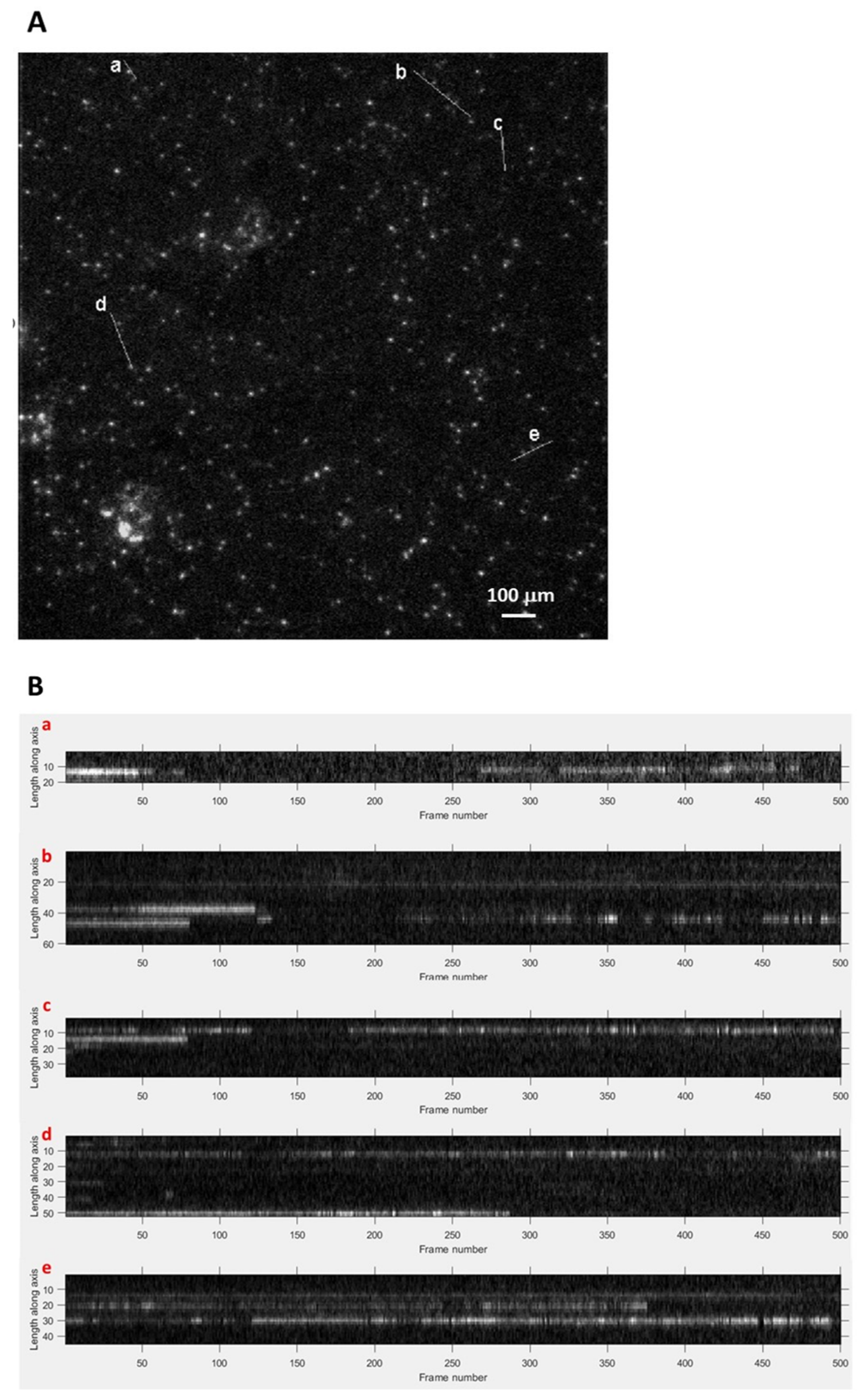
3.3. Total Internal Reflection Fluorescence Microscope (TIRF)

Figure 10 shows the optical properties of PbS QDs at the single molecule level. The PbS QDs adsorbed on the surface of the coverslip are observed with total internal reflection fluorescence (TIRF) microscopy at room temperature (22 °C). Emission signals of PbS QDs excited with a 532 nm DPSS laser (Cobolt Samba, Hubner Photonics, Solna, Sweden), 15 mW, were imaged by a TIRF microscope (IX-71, Olympus, Tokyo, Japan, oil-immersion 100× objective) and recorded using EMCCD (ImagEM C9100-13, Hamamatsu, photonics, Hertfordshire, UK) and MetaMorph 7.6 (Molecular Devices, San Jose, CA, USA) imaging software at a 50 ms time resolution. The data were analyzed using DiaTrack 3.05 (Pascal Vallotton, Zurich, Switzerland) and ImageJ (1.53t 24, National Institute of Health, Bethesda, MD, USA).
The kymographs shown in Figure 10B display the lifetime of fluorescence of individual QD highlighted by the lines (a, b, c, d and e) on Figure 10A. Each kymograph consists of 500 consecutive images of the selected QDs. The ON (the white spots) and OFF (the black spots) states of the fluorescence are clearly shown by the kymographs.
PbS QDs have shown intermittent fluorescence or blinking phenomena (unsystematic switching between emitting and non-emitting states) attributed to Auger recombination or surface trap-induced recombination.

4. Conclusions

A heterojunction has been constructed composed of PbS quantum dots and ZnO nanowires for a quantum dot-sensitized solar cell which is expected to improve charge transfer and boost the efficiency of the solar cell.
PbS NPs have been embedded within ZnO NWs using the Successive Ionic Layer Adsorption and Reaction (SILAR) technique with no organic materials. The effect of the number of SILAR cycles on the density and the sizes of the NPs has been investigated. The grown NPs were crystalline, which was confirmed by XRD and TEM. The ZnO NWs were treated by plasma ashing to improve their wettability properties.
Our research has demonstrated that the SILAR technique can be used effectively to synthesize quantum dots at different densities and sizes on the surface of ZnO nanowires with high quality, and should be considered as the building block for solar cells.

5. Patents

This work is based on our patent number “US 2015/0280017 A1”.

Author Contributions

Conceptualization, B.E., M.A., A.S.B., M.I.A., E.D. and G.E.J.; Data curation, M.A., A.A.-K., M.I.A. and S.M.H.; Formal analysis, M.A., A.S.B., A.A.-K., M.I.A. and S.M.H.; Funding acquisition, G.E.J.; Investigation, B.E., M.A., A.S.B., A.A.-K., M.I.A. and S.M.H.; Methodology, B.E., M.A., A.S.B., A.A.-K., M.I.A. and S.M.H.; Project administration, E.D.; Resources, B.E.; Supervision, E.D. and G.E.J.; Writing – original draft, B.E.; Writing – review and editing, M.A., A.S.B., A.A.-K., M.I.A., S.M.H., E.D. and G.E.J. All authors have read and agreed to the published version of the manuscript.

Funding

This research received no external funding.

Institutional Review Board Statement

Not applicable.

Informed Consent Statement

Not applicable.

Data Availability Statement

Data sharing is not applicable to this article.

Conflicts of Interest

The authors declare no conflict of interest.

References

  1. Grätzel, M. Photoelectrochemical cells. Nature 2001, 414, 338–344. [Google Scholar] [CrossRef]
  2. Wang, Z.; Hu, T.; Liang, R.; Wei, M. Application of Zero-Dimensional Nanomaterials in Biosensing. Front. Chem. 2020, 8, 320. [Google Scholar] [CrossRef] [PubMed]
  3. Nozik, A.J. Multiple exciton generation in semiconductor quantum dots. Chem. Phys. Lett. 2008, 457, 3–11. [Google Scholar] [CrossRef]
  4. Kumar, K.; Kumar, A.; Devi, S.; Tyagi, S.; Kaur, D. Relevant photovoltaic effect in N-doped CQDs/MoS2 (0D/2D) quantum dimensional heterostructure. Ceram. Int. 2022, 48, 14107–14116. [Google Scholar] [CrossRef]
  5. Damtie, F.A.; Karki, K.J.; Pullerits, T.; Wacker, A. Optimization schemes for efficient multiple exciton generation and extraction in colloidal quantum dots. J. Chem. Phys. 2016, 145, 064703. [Google Scholar] [CrossRef] [Green Version]
  6. Yang, P.; Yan, R.; Fardy, M. Semiconductor Nanowire: What’s Next? Nano Lett. 2010, 10, 1529–1536. [Google Scholar] [CrossRef]
  7. Navarro Yerga, R.M.; Álvarez Galván, M.C.; Del Valle, F.; Villoria de la Mano, J.A.; Fierro, J.L. Water Splitting on Semiconductor Catalysts under Visible-Light Irradiation. ChemSusChem 2009, 2, 471–485. [Google Scholar] [CrossRef] [PubMed]
  8. Raheman Ar, S.; Wilson, H.M.; Momin, B.M.; Annapure, U.S.; Jha, N. CdSe quantum dots modified thiol functionalized g-C3N4: Intimate interfacial charge transfer between 0D/2D nanostructure for visible light H2 evolution. Renew. Energy 2020, 158, 431–443. [Google Scholar] [CrossRef]
  9. Yang, Z.; Zhang, J.; Kintner-Meyer, M.C.W.; Lu, X.; Choi, D.; Lemmon, J.P.; Liu, J. Electrochemical Energy Storage for Green Grid. Chem. Rev. 2011, 111, 3577–3613. [Google Scholar] [CrossRef]
  10. Trinh, M.T.; Polak, L.; Schins, J.M.; Houtepen, A.J.; Vaxenburg, R.; Maikov, G.I.; Grinbom, G.; Midgett, A.G.; Luther, J.M.; Beard, M.C.; et al. Anomalous Independence of Multiple Exciton Generation on Different Group IV−VI Quantum Dot Architectures. Nano Lett. 2011, 11, 1623–1629. [Google Scholar] [CrossRef]
  11. Fan, Z.; Ruebusch, D.J.; Rathore, A.A.; Kapadia, R.; Ergen, O.; Leu, P.W.; Javey, A. Challenges and prospects of nanopillar-based solar cells. Nano Res. 2009, 2, 829. [Google Scholar] [CrossRef] [Green Version]
  12. Yu, J.; Yang, H.; Shi, R.; Zhang, L.; Zhao, H.; Wang, X. Vapor–liquid–solid growth and narrow-band ultraviolet photoluminescence of well-aligned GeO2 nanowire arrays with controllable aspect ratios. Appl. Phys. A 2010, 100, 493–499. [Google Scholar] [CrossRef]
  13. Garnett, E.; Yang, P. Light Trapping in Silicon Nanowire Solar Cells. Nano Lett. 2010, 10, 1082–1087. [Google Scholar] [CrossRef] [PubMed]
  14. Law, M.; Greene, L.E.; Johnson, J.C.; Saykally, R.; Yang, P. Nanowire dye-sensitized solar cells. Nat. Mater. 2005, 4, 455–459. [Google Scholar] [CrossRef]
  15. Mosquera, E.; Morel, M.J.; Diosa, J.E. Catalyst-free growth of ZnO nanowires: Structural, optical, vibrational and field emission properties. Appl. Phys. A 2019, 125, 613. [Google Scholar] [CrossRef]
  16. Wang, Y.; Li, D.; Chao, L.; Niu, T.; Chen, Y.; Huang, W. Perovskite photodetectors for flexible electronics: Recent advances and perspectives. Appl. Mater. Today 2022, 28, 101509. [Google Scholar] [CrossRef]
  17. Nahar Myyas, R.e.; Al-Dabbasa, M.; Tostado-Véliz, M.; Jurado, F. A novel solar panel cleaning mechanism to improve performance and harvesting rainwater. Sol. Energy 2022, 237, 19–28. [Google Scholar] [CrossRef]
  18. Huang, C.-T.; Song, J.; Lee, W.-F.; Ding, Y.; Gao, Z.; Hao, Y.; Chen, L.-J.; Wang, Z.L. GaN Nanowire Arrays for High-Output Nanogenerators. J. Am. Chem. Soc. 2010, 132, 4766–4771. [Google Scholar] [CrossRef] [PubMed]
  19. Consonni, V.; Briscoe, J.; Kärber, E.; Li, X.; Cossuet, T. ZnO nanowires for solar cells: A comprehensive review. Nanotechnology 2019, 30, 362001. [Google Scholar] [CrossRef] [PubMed]
  20. Ozu, S.; Zhang, Y.; Yasuda, H.; Kitabatake, Y.; Toyoda, T.; Hirata, M.; Yoshino, K.; Katayama, K.; Hayase, S.; Wang, R.; et al. Improving Photovoltaic Performance of ZnO Nanowires Based Colloidal Quantum Dot Solar Cells via SnO2 Passivation Strategy. Front. Energy Res. 2019, 7, 11. [Google Scholar] [CrossRef]
  21. Ponzoni, A.; Comini, E.; Sberveglieri, G.; Zhou, J.; Deng, S.Z.; Xu, N.S.; Ding, Y.; Wang, Z.L. Ultrasensitive and highly selective gas sensors using three-dimensional tungsten oxide nanowire networks. Appl. Phys. Lett. 2006, 88, 203101. [Google Scholar] [CrossRef] [Green Version]
  22. Opoku, C.; Dahiya, A.S.; Oshman, C.; Cayrel, F.; Poulin-Vittrant, G.; Alquier, D.; Camara, N. Fabrication of ZnO Nanowire Based Piezoelectric Generators and Related Structures. Phys. Procedia 2015, 70, 858–862. [Google Scholar] [CrossRef] [Green Version]
  23. Le, A.T.; Ahmadipour, M.; Pung, S.-Y. A review on ZnO-based piezoelectric nanogenerators: Synthesis, characterization techniques, performance enhancement and applications. J. Alloy. Compd. 2020, 844, 156172. [Google Scholar] [CrossRef]
  24. Gemeda, G.F.; Etefa, H.F.; Hsieh, C.-C.; Kebede, M.A.; Imae, T.; Yen, Y.-W. Preparation of ZnO/NiO-loaded flexible cellulose nanofiber film electrodes and their application to dye-sensitized solar cells. Carbohydr. Polym. Technol. Appl. 2022, 3, 100213. [Google Scholar] [CrossRef]
  25. Yan, R.; Gargas, D.; Yang, P. Nanowire photonics. Nat. Photonics 2009, 3, 569–576. [Google Scholar] [CrossRef]
  26. Rodwihok, C.; Choopun, S.; Ruankham, P.; Gardchareon, A.; Phadungdhitidhada, S.; Wongratanaphisan, D. UV sensing properties of ZnO nanowires/nanorods. Appl. Surf. Sci. 2019, 477, 159–165. [Google Scholar] [CrossRef]
  27. Caicedo, N.; Leturcq, R.; Raskin, J.-P.; Flandre, D.; Lenoble, D. Detection mechanism in highly sensitive ZnO nanowires network gas sensors. Sens. Actuators B Chem. 2019, 297, 126602. [Google Scholar] [CrossRef]
  28. Campos, A.C.; Paes, S.C.; Correa, B.S.; Cabrera-Pasca, G.A.; Costa, M.S.; Costa, C.S.; Otubo, L.; Carbonari, A.W. Growth of Long ZnO Nanowires with High Density on the ZnO Surface for Gas Sensors. ACS Appl. Nano Mater. 2020, 3, 175–185. [Google Scholar] [CrossRef] [Green Version]
  29. Plass, R.; Pelet, S.; Krueger, J.; Grätzel, M.; Bach, U. Quantum Dot Sensitization of Organic−Inorganic Hybrid Solar Cells. J. Phys. Chem. B 2002, 106, 7578–7580. [Google Scholar] [CrossRef]
  30. Chang, C.-H.; Lee, Y.-L. Chemical bath deposition of CdS quantum dots onto mesoscopic TiO2 films for application in quantum-dot-sensitized solar cells. Appl. Phys. Lett. 2007, 91, 053503. [Google Scholar] [CrossRef]
  31. Chen, S.; Truax, L.A.; Sommers, J.M. Alkanethiolate-Protected PbS Nanoclusters:  Synthesis, Spectroscopic and Electrochemical Studies. Chem. Mater. 2000, 12, 3864–3870. [Google Scholar] [CrossRef]
  32. He, Y.; Ouyang, T.; Ouyang, G. Shape-modulated multiple exciton generation and optoelectronic properties in PbSe nanostructures. J. Appl. Phys. 2018, 124, 184302. [Google Scholar] [CrossRef]
  33. Qu, Y.; Duan, X. One-dimensional homogeneous and heterogeneous nanowires for solar energy conversion. J. Mater. Chem. 2012, 22, 16171–16181. [Google Scholar] [CrossRef]
  34. Hines, M.A.; Scholes, G.D. Colloidal PbS Nanocrystals with Size-Tunable Near-Infrared Emission: Observation of Post-Synthesis Self-Narrowing of the Particle Size Distribution. Adv. Mater. 2003, 15, 1844–1849. [Google Scholar] [CrossRef]
  35. Konstantatos, G.; Levina, L.; Fischer, A.; Sargent, E.H. Engineering the Temporal Response of Photoconductive Photodetectors via Selective Introduction of Surface Trap States. Nano Lett. 2008, 8, 1446–1450. [Google Scholar] [CrossRef]
  36. Choi, H.; Nicolaescu, R.; Paek, S.; Ko, J.; Kamat, P.V. Supersensitization of CdS Quantum Dots with a Near-Infrared Organic Dye: Toward the Design of Panchromatic Hybrid-Sensitized Solar Cells. ACS Nano 2011, 5, 9238–9245. [Google Scholar] [CrossRef]
  37. Soonmin, H. Recent Advances in the Growth and Characterizations of SILAR-Deposited Thin Films. Appl. Sci. 2022, 12, 8184. [Google Scholar] [CrossRef]
  38. Lee, W.; Yeop, J.; Heo, J.; Yoon, Y.J.; Park, S.Y.; Jeong, J.; Shin, Y.S.; Kim, J.W.; An, N.G.; Kim, D.S.; et al. High colloidal stability ZnO nanoparticles independent on solvent polarity and their application in polymer solar cells. Sci. Rep. 2020, 10, 18055. [Google Scholar] [CrossRef]
  39. Wibowo, A.; Marsudi, M.A.; Amal, M.I.; Ananda, M.B.; Stephanie, R. ZnO nanostructured materials for emerging solar cell applications. RSC Adv. 2020, 10, 42838–42859. [Google Scholar] [CrossRef]
  40. Raha, S.; Ahmaruzzaman, M. ZnO nanostructured materials and their potential applications: Progress, challenges and perspectives. Nanoscale Adv. 2022, 4, 1868–1925. [Google Scholar] [CrossRef]
  41. ElZein, B.; Yao, Y.; Barham, A.S.; Dogheche, E.; Jabbour, G.E. Toward the Growth of Self-Catalyzed ZnO Nanowires Perpendicular to the Surface of Silicon and Glass Substrates, by Pulsed Laser Deposition. Materials 2020, 13, 4427. [Google Scholar] [CrossRef]
  42. Nguyen, T.-L.; Michael, M.; Mulvaney, P. Synthesis of Highly Crystalline CdSe@ZnO Nanocrystals via Monolayer-by-Monolayer Epitaxial Shell Deposition. Chem. Mater. 2014, 26, 4274–4279. [Google Scholar] [CrossRef]
  43. Li, R.; Wei, Z.; Zhao, F.; Gao, X.; Fang, X.; Li, Y.; Wang, X.; Tang, J.; Fang, D.; Wang, H.; et al. Investigation of localized and delocalized excitons in ZnO/ZnS core-shell heterostructured nanowires. Nanophotonics 2017, 6, 1093–1100. [Google Scholar] [CrossRef]
  44. Takahashi, A.; Wang, H.; Fukuda, T.; Kamata, N.; Kubo, T.; Segawa, H. Annealing-Temperature Dependent Carrier-Transportation in ZnO/PbS Quantum Dot Solar Cells Fabricated Using Liquid-Phase Ligand Exchange Methods. Energies 2020, 13, 5037. [Google Scholar] [CrossRef]
Figure 1. Schematic illustration of nanowires during (a) light trapping and (b) electron transport to electrodes.
Coatings 12 01486 g001
Figure 2. Illustration of the operation of quantum dot-sensitized solar cells, reflecting the charge injection from the absorber (PbS) into electron transport layer (ZnO).
Coatings 12 01486 g002
Figure 3. Illustration of ZnO nanowires decorated with PbS NPs forming a radial junction.
Coatings 12 01486 g003
Figure 4. The scheme of PbS thin-film deposition (○Pb2+; S2−) by SILAR: (a) Pb2+ cationic precursor, (b) ion exchange water, (c) S2− anionic precursor and (d) ion exchange water.
Coatings 12 01486 g004
Figure 5. SEM images of ZnO NWs grown by PLD Top (a,c,e,g) and tilted (b,d,f,h) view; (a,b) before PbS deposition, and (ch) after PbS deposition for different cycles: (c,d) after 5 SILAR cycles, (e,f) after 10 SILAR cycles and (g,h) after 16 SILAR cycles.
Coatings 12 01486 g005aCoatings 12 01486 g005b
Figure 6. Low- and high-resolution TEM images demonstrate the configuration of the PbS-QD/ZnO NWs. Corresponding FFT patterns reveal the ordering of the super lattices of (a) PbS deposition for 16 SILAR cycles (b) PbS deposition for 10 SILAR cycles, and (c) PbS deposition for 5 SILAR cycles.
Coatings 12 01486 g006
Figure 7. (a) PL spectra of the ZnO NWs decorated with PbS NPs synthesized at different SILAR cycles and (b) NBE wavelength of the ZnO NWs decorated with PbS NPs in relation to the number of cycles.
Coatings 12 01486 g007
Figure 8. XRF spectra of the ZnO/PbS heterostructure at different concentrations.
Coatings 12 01486 g008aCoatings 12 01486 g008b
Figure 9. XRD pattern of ZnO/PbS heterojunction: 5 cycles and 10 cycles.
Coatings 12 01486 g009
Figure 10. Optical characterization and photophysical properties of PbS QDs adsorbed on a glass coverslip. (A) The 1st TIRF image of PbS QDs extracted from a time lapse movie (λexc. = 532 nm). (B) Representative kymograph displaying the lifetime of fluorescence of individual particles present on the lines (a, b, c, d and e) highlighted on Figure 10A.
Coatings 12 01486 g010
Table 1. Parameters used for SILAR.
SamplePbCl2 (mg)Na2S (mg)Dipping TimeNumber of Cycles
S A18.45.2170s5 cycles
S B18.45.2170s10 cycles
S C18.45.2170s16 cycles
Table 2. Summary of PbS NPs sizes deposited for different numbers of cycles.
SampleNumber of CyclesPbS NPs Size Spherical Shape
A5~3.1–4.3 nm
B10~4.7–6 nm
C16~7–9 nm
Table 3. D spacing identified by TEM and its corresponding plane.
D (A°)Plane
3.5(111)
2.53(200)
2.12(220)
Table 4. Theoretical bandgaps based on the size of the QDs.
Number of CyclesPBS NP Size (NM)EG (EV)
16~7–90.66
10~4.7–60.863
5~3.1–4.31.13
Publisher’s Note: MDPI stays neutral with regard to jurisdictional claims in published maps and institutional affiliations.

