Article

Effect of Target Sintering Temperature on the Morphological and Optical Properties of Pulsed Laser Deposited TiO2 Thin Films

1
Laboratoire de Microscopie Electronique et Sciences des Matériaux (LMESM), Département de Technologie des Matériaux, Faculté de Physique, Université des Sciences et de la Technologie d’Oran Mohamed Boudiaf (USTO-MB), El M’naouar BP 1505, Bir El Djir, Oran 31000, Algeria
2
Science Research Department, Institute of Interdisciplinary Research, Research Center in Environmental Sciences for the North-Eastern Romanian Region (CERNESIM), AlexandruIoan Cuza University of Iasi, Bulevardul Carol I, Nr. 11, 700506 Iasi, Romania
3
National Institute of Research and Development for Technical Physics, 47 Mangeron Boulevard, 700050 Iasi, Romania
4
LOA-SL, Faculty of Physics, AlexandruIoan Cuza University of Iasi, Bulevardul Carol I, Nr. 11, 700506 Iasi, Romania
5
Faculty of Physics, AlexandruIoan Cuza University of Iasi, Bulevardul Carol I, Nr. 11, 700506 Iasi, Romania
*
Authors to whom correspondence should be addressed.
Coatings 2021, 11(5), 561; https://doi.org/10.3390/coatings11050561
Submission received: 31 March 2021 / Revised: 4 May 2021 / Accepted: 6 May 2021 / Published: 11 May 2021
(This article belongs to the Special Issue Optical Thin Films: Preparation, Application and Development)

Abstract

:
In this paper, we report on the effect of titanium dioxide (TiO2) target sintering temperature on the morphological and optical properties of amorphous titanium dioxide thin films synthesized by pulsed laser deposition (PLD) on indium tin oxide (ITO) glass substrate and subsequently heat-treated in air at low temperature (150 °C). Three types of targets were used, unsintered (pressed at room temperature), sintered at 500 °C and sintered at 1000 °C. The surface morphology of the samples was investigated by scanning electron microscopy (SEM), and profilometry was used for thickness measurements. The structural properties of the films were examined by X-ray diffraction (XRD), while their optical properties were studied by UV‒vis spectroscopy. The obtained TiO2 thin films have an amorphous nature, as shown by XRD analysis. Profilometer showed that sintered target samples have more reliable thicknesses than unsintered ones. The SEM studies revealed the sufficient structural homogeneity of sintered target nanosized TiO2 films and agglomerates in the case of unsintered target film. The UV‒vis transmittance spectra showed high transparency in the visible range of PLD films, proportional to the target sintering temperature. The optical band gaps of the films deposited using the 500 °C and 1000 °C sintered targets are closer to those of anatase and rutile phases, respectively, which provides a promising approach to the challenges of amorphous TiO2-based nanostructures.

1. Introduction

Titanium dioxide (TiO2) in thin films has been extensively used in a wide range of applications, such as sensors, self-cleaning, protective or antireflective layers, electrodes in electrochromic devices, electron transport layers in emerging photovoltaic cells (dye-sensitized, perovskite and polymeric cells), photocatalysts, pigments, etc., due to its high transparency across the visible spectrum, appropriate band gap, effective charge separation ability, low toxicity and low price [1,2,3,4,5,6,7,8]. Titanium dioxide (titania) also displays abundant surface hydroxyl (OH) groups, high defect density and enhanced absorption in the ultraviolet (UV) range, such as UV materials [9,10,11,12,13].
Titania is a n-type semiconductor material and displays three stable polymorphic forms: anatase (tetragonal), rutile (tetragonal) and brookite (orthorhombic) phases, which provide flexibility and versatility in applications [8,14]. At increased temperatures (~500 °C), amorphous TiO2 transforms to crystalline anatase, and at temperatures higher than about ~700 °C to 800 °C, to rutile phase. The transformation to rutile phase is irreversible, and the melting point of TiO2 is 1858 °C [8,14,15]. Furthermore, the currently known methods to crystallize amorphous TiO2 films into anatase or rutile phases require the annealing step, including oxygen plasma treatment [16,17,18]. Anatase crystals exhibit excellent optical properties, higher photocatalytic activity and gas sensing properties than rutile ones, and a lower electron–hole recombination rate. Further, the band gap of anatase phase (3.2 eV) is larger than that of rutile (3.0 eV), and the charge carrier mobility is higher [16,19]. However, rutile phase is more thermodynamically stable and durable than anatase, while brookite is not commonly studied because it is difficult to prepare due to its metastability [15,20,21]. The transport mechanism of carriers (electrons and holes) in titania can be improved in the case of mixed-phase TiO2 (rutile-anatase), which exhibits higher photocatalytic activity [16].
Although amorphous TiO2 films have numerous advantages, including simple synthesis conditions and a larger surface area, allowing the integration of more chemicals and compatibility with the largest variety of substrates [1,22], they are much less studied compared to crystalline (anatase or rutile phases) films. In addition, the oxygen vacancies and disordered arrangement of intrinsic atoms have important effects on the electronic structure, which could improve the separation efficiency and transfer of photogenerated charge carriers [22,23,24]. Moreover, the electronic structure and optical properties of amorphous TiO2 are much closer to those of anatase TiO2 [24]. A new approach to TiO2 thin film exploration and applications was provided by Addonizio et al. [1], Kim et al. [17] and Sun et al. [24].
Various methods have been used to obtain TiO2 thin films, such as electron beam evaporation [25], radiofrequency (RF) magnetron sputtering [26], chemical vapor deposition [27], sol–gel technique [28], and pulsed laser deposition (PLD) [29,30]. The properties of deposited films are highly dependent on the processing techniques and the deposition conditions [31]. Pulsed laser deposition offers several benefits: the simple system operation, flexibility, a wide range of deposition conditions, rich choice of materials, the possibility to use in situ heating and reactive background gases, and a relatively high reproducibility [8,19,32,33]. This technique also allows the deposition of films with determined thickness, morphology, stoichiometry, grain size and composition by varying the deposition parameters (laser pulse geometry, laser fluence, wavelength or repetition frequency, target-substrate distance, substrate temperature, deposition time, etc.) [11,34,35]. The composition, purity and density (sintering temperature) of the bulk target have an important influence on the quality of laser ablated films [36]. Furthermore, in vacuum, PLD provides compact and continuous films, whereas porous structures can be achieved at relatively high background gas pressures [37].
In this study, we report the successful synthesis of nanosized amorphous TiO2 films by PLD on indium tin oxide (ITO) glass substrate (due to their high visible transmittance, among transparent conducting oxides materials [38]) at room temperature (25 °C), without reactive background gases, from two targets sintered at different temperatures (500 °C and 1000 °C) and an unsintered one (25 °C), as-deposited films were then thermally treated at 150 °C for 30 min. The study of PLD-synthesized amorphous nanosized TiO2 thin films is still poorly reported in the literature. The influence of target sintering temperature on the morphological and optical properties was investigated by scanning electron microscopy (SEM) and UV‒vis spectroscopy, respectively. The obtained thin films may not only display a satisfactory uniformity and highly transparent TiO2 nanostructures via low-temperature processing, but also exhibit similar optical properties to those of crystalline TiO2.

2. Experimental Details

The experimental setup used for pulsed laser deposition of TiO2 films is similar to that described in [39]. The disk-shaped targets with ~20 mm diameter and about 2 mm thickness were prepared from commercially available high purity (>99.50%) titanium (IV) oxide powder (BIOCHEM Chemopharma; product code: 320150500). The powder was ground in an agate mortar and pressed at 2 MPa. Three targets were used for deposition: one target was prepared at room temperature (25 °C), while two others were sintered in air for 5 h (one at 500 °C and the second at 1000 °C, both with a 10 °C/min heating rate), using a Apriltherm 5L furnace. The films were deposited on ITO (thickness: ~150 nm, sheet resistance: ~10 Ω/sq, transmittance > 80% and with (400) texture)-coated glass substrates (10 mm × 15 mm × 1 mm), which were ultrasonically cleaned using acetone for 10 min and dried in air before loading them into the PLD chamber. Three thin-film samples were used, labeled as as 25-TiO2, as 500-TiO2 and as 1000-TiO2, according to the target sintering temperature. All the depositions were performed at room temperature without reactive background gases, using the experimental parameters shown in Table 1. The targets were rotated during the laser irradiation in order to avoid the formation of deep surface craters [16]. Thermal treatments (5 °C/min heating rate, 30 min dwell at 150 °C) were performed ex situ on the as-deposited samples to ensure good adherence and compactness, and to moderate the transmittance of the titania films. Heat-treated samples were labeled similarly, as ptt 25-TiO2, ptt 500-TiO2 and ptt 1000-TiO2.
The thickness of thin-film samples under study was measured with a Dektak XT stylus profilometer (Bruker, Paris, France) with a resolution of 1 nm, while the morphological properties of the films were studied by SEM (JSM 6390/JEOL apparatus at 30 kV accelerating voltage). The UV‒vis transmittance spectra of the films in the 300–900 nm wavelength range were recorded using a UV‒vis Avantes spectrometer (AvaSpec 2048, Schiphol, The Netherlands). The XRD patterns in the 10–80° 2θ range were obtained using a Shimadzu LabX XRD-6000 diffractometer (Shimadzu, Kyoto, Japan) with a CuKα radiation (λ = 1.54 Å) and further used in structural analysis of samples. The diffractograms were recorded with a scanning angle step of 0.02° and 1°/min scan speed.

3. Results and Discussion

3.1. Morphological Properties

Figure 1 shows the influence of target sintering temperature on the film thickness. The thickness of three thin-film samples, as 25-TiO2, as 500-TiO2 and as 1000-TiO2, were found to be approximately equal to 67, 47 and 34 nm, respectively. The lower thickness of the as 500-TiO2 and as 1000-TiO2 films compared to that of as 25-TiO2 one could be due to the greater density (high sintered temperature) of sintered targets compared to that of the unsintered one (i.e., the films obtained from higher density targets are more compact than those prepared from the sparse one, containing agglomerations, which can affect the accuracy of the film thickness measurement).However, the films obtained from sintered targets had slight differences in the thickness. Consequently, the thicknesses of sintered targets films were determined more accurately than in the case of unsintered one.
Scanning electron microscopy micrographs of TiO2 samples grown on ITO glass substrates were acquired to study the thin-film morphology (Figure 2). The as 25-TiO2 (Figure 2a) film displays a granular structure, with significant agglomerates (white particulates) and weak small cracks. The as 500-TiO2 (Figure 2b) and as 1000-TiO2 (Figure 2c) samples display relatively uniform and flat surfaces composed of small irregular-shaped grains, with slight agglomerates in the case of as 500-TiO2. The presence of agglomerates can be attributed to the sparse target or lower density [36]. However, the reason for these small cracks is still not very clear. They may result from the presence of agglomerates combined with lower thickness of the film (i.e., in some cases, the particulates larger than film thickness, as shown by profilometry, can affect the film adhesion).
After thermal treatment for 30 min at 150 °C, the ptt 25-TiO2 (Figure 2d), ptt 500-TiO2 (Figure 2e) and ptt 1000-TiO2 (Figure 2f) films were not distinctively changed, except for the reduction in agglomerates. The morphology of the agglomerates was influenced by the heat treatment, resulting in a reduction [40], while the slight change in the films morphology is due to the low temperature treatment [1,41].

3.2. Structural Properties

Figure 3a shows the XRD patterns of TiO2 unsintered and sintered targets at 1000 °C. It clearly indicates the transformation of the anatase phase (anatase TiO2, ICSD file no. 01-089-4921) with particle sizes of 47.9 nm dominant in the unsintered target (25 °C) of TiO2 to the rutile phase (Rutile TiO2-ICSD file no. 01-087-0710) with particle sizes of 41.7 nm in the 1000 °C sintered target, due to the high sintering temperature, according to the current literature [14,15]. However, in the unsintered target, Ti3O5 peaks (Ti3O5-PDF file no. 96-152-7091) are also observed as secondary phases, which could be converted partially to Ti6O (Ti6O-ICSD file no. 01-072-1471) in the target sintered at 1000 °C, due to the oxygen deficiency during the sintering process [20].
On the other hand, the XRD patterns of the samples and ITO glass substrate before and after heat treatment at 150 °C for 30 min are presented in Figure 3b,c, respectively. It can be clearly noticed that the ITO (ITO-ICSD file no. 01-089-4596) glass substrates exhibit the (400) preferred orientation, and consequently, this plane contains more oxygen vacancies than the (222) one [42]. As can be easily observed, all diffractograms exhibit no obvious diffraction peak except those corresponding to the ITO glass substrate, suggesting that nanosized TiO2 films under study, both untreated and heat treated, are amorphous. The broad amorphous halo between 15° and 40° is mainly due to the amorphous glass substrate, as well as to the amorphous TiO2 phase. The thermal treatment of titania thin-film samples, conducted at 150 °C for 30 min, is most likely not sufficient to result in a detectable crystallization [1].

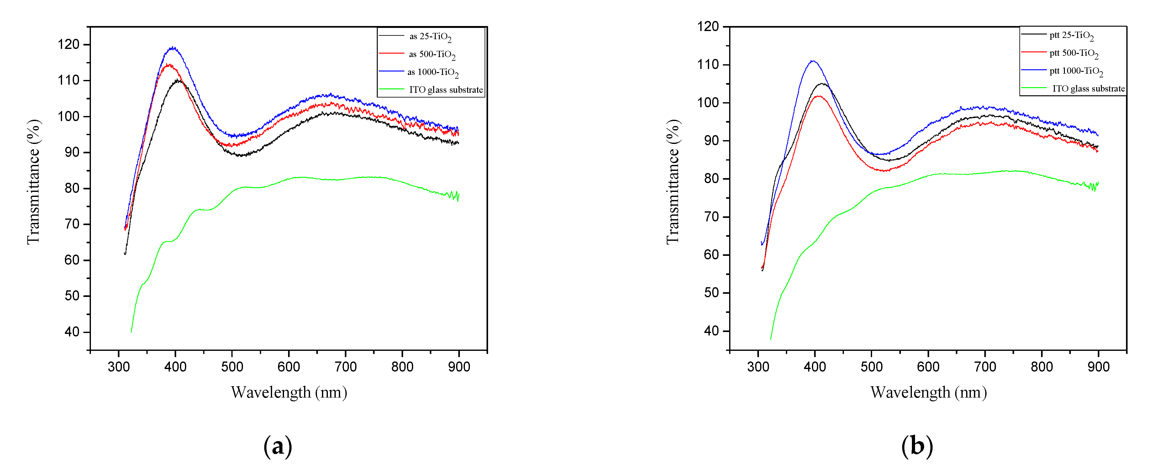
3.3. Optical Properties

In order to investigate the effect of target sintering temperatures on the optical properties of titanium dioxide thin films, optical transmittance and optical band gap studies were performed in the UV−visible region.
Figure 4 shows the UV−vis transmittance spectra of TiO2 thin films and ITO glass substrate reference before (Figure 4a) and after thermal treatment (Figure 4b). In the spectral range from 300 nm to 400 nm, the transmittances increased from 60% to 120% and from 55% to 110% for as deposited and post-thermally treated films, respectively. The transmissions were approximately 100% for as-deposited films and 95% for thermally treated films in the visible range. The transmission of as-deposited films in the visible range can be conditioned by the large band gap of amorphous TiO2 [1]. However, the transmission in the UV region and high transmission in the visible range, particularly that which exceeds 100%, remain ambiguous. This can be explained by sample photoluminescence, PL (i.e., when irradiated, TiO2 nanostructures exhibit luminescence emission, which may increase the transmittance intensity), which is strongly related to the presence of surface states and defects [41], whereas amorphous TiO2 displays high defect density and disordered arrangement, as mentioned in the introduction. Moreover, amorphous TiO2 nanoparticles exhibit a green PL band that is almost always visible, and highlighted the potential for PL-based applications using amorphous TiO2 nanoparticles [41]. As a result, and more often, one can observe PL emissions in the UV region of transmittance spectra. Thus, TiO2 thin films display originally high transmittance in the visible range, and nanostructured TiO2 thin films are able to emit a luminescence spectrum under light excitation, which can result in transmittance intensities higher than 100%. The oscillations present (two main bands with maxima in the visible range) in transmittance spectra of both untreated and thermally treated films are interference-based effects (interference of reflected light from both faces of the film) [43]. The interference fringes suggest that examined films are optically plane, homogeneous and display smooth surfaces [15,43]. In the UV−vis region, the transmittance of TiO2 films, thermally treated at 150 °C for 30 min, decreased slightly compared to that of the as-deposited films, and became reasonable in the visible spectrum range, due to scattering enhancement after thermal treatment [44]. Additionally, the transmittance of ptt500-TiO2 film was found to decrease more sharply compared to the others. This decrease might be the result of the increased surface roughness of thinner films, in the presence of mentioned cracks and agglomerations. The films from sintered targets exhibit slightly higher transmittance than those prepared at the room temperature (25 °C) pressed target, owing to their lower thickness [45]. Hence, the optical transmittance is proportional to the target sintering temperature.
The optical band gap, Eg, was calculated using the Tauc equation for indirect transitions [22,46]:
( α h ν ) 1 / 2 = k ( h ν Eg )
where α denotes the optical absorption coefficient, defined as   α = [ 1 d ln ( 1 T ) ] (under the assumption of a negligible reflectance, R<<1), d is the film thickness, T is the transmittance, h ν   is the photon energy and k is a constant. The optical band gap was estimated at the absorption edge, by extrapolating the linear part of the ( α h ν ) 1 / 2 = f ( h ν )   plots to zero absorption [43], as shown in Figure 4c,d for as-deposited and thermally treated thin films, respectively. The estimated band gaps (Eg) are summarized in Table 2.
As can be inferred from the data listed in Table 2, the Eg values of the as-deposited amorphous nanosized TiO2 films ranged between 3.25 eV and 3.35 eV, in good agreement with those reported by Zhang et al. [43] and Addonizio et al. [1] for amorphous TiO2 films. After thermal treatment, the Eg value of the compact layers deposited from sintered targets decreased due to the change in the thin-film nanostructure (density) [44]. On the contrary, ptt 25-TiO2 showed a slight increase in Eg value, which could be caused by an artifact of the nanostructure [15]. As one can observe, the optical band gap of ptt 500-TiO2 film (3.17 eV) is closer to that of anatase TiO2 {3.20 eV [47]}, confirmed by Sirgh et al. [48] and Sun et al. [24], while the Eg value of ptt1000-TiO2(3.06 eV) is much closer to that of rutile TiO2 {3.02−3.05 eV[47]}. In this way, amorphous TiO2-based nanostructures can provide a promising method for overcoming crystalline titania crystalline-related challenges.

4. Conclusions

In this work, the properties of TiO2 thin films deposited by the PLD technique were examined. The effect of target sintering temperature on the morphological and optical characteristics of titania thin films was investigated in detail. The results showed that amorphous nanosized TiO2 films from sintered targets can be successfully prepared via PLD with actual deposition parameters. Profilometer measurements demonstrated that TiO2 thin film thicknesses obtained from sintered targets are more reliable than those obtained from unsintered target. SEM characterization revealed flat and relatively good homogeneity of the nanosized films from sintered targets, and the presence of small cracks and agglomerates in the film from the unsintered target. A correlation between the target sintering temperature and film morphology was observed: thinner films from higher sintering temperature targets (more than 500 °C) can assure good adherence of the titania films; however, sparse targets (below 500 °C) provoke agglomerate formation on the film surfaces. The low temperature thermal treatment (30 min at 150 °C) of the nanosized TiO2 films led to a reduction in particulates in the film prepared from unsintered target. The TiO2 thin films exhibited high transparency in the visible range, which corresponded to the large band gap and was proportional to the sintering temperature of target. In addition, the optical transmission was moderate in the visible range, and the optical band gaps of the films prepared from 500 °C and 1000 °C sintered targets were found to be similar to those of anatase and rutile TiO2 phases, respectively, which offers a promising perspective on the challenges of amorphous TiO2-based nanostructures.

Author Contributions

Conceptualization, L.K.; Data curation, L.K., G.B., A.C., S.G. (Stoian Geroge) and C.D.; Investigation, L.K., L.L., A.C.; Resources, G.B., A.C., S.G. (Stoian George), S.G. (Silviu Gurlui), L.L. and C.D.; Supervision, S.G. (Stoian George), L.L., C.D. and M.A.; Writing—original draft, L.K.; Writing—review & editing, G.B., A.C., L.L., C.D. and M.A. All authors have read and agreed to the published version of the manuscript.

Funding

This research was funded by Ministry of Research, Innovation and Digitization, project FAIR_09/24.11.2020 and by the Executive Agency for Higher Education, Research, Development, and Innovation, UEFISCDI, ROBIM- project number PN-III-P4-ID-PCE2020-0332.

Institutional Review Board Statement

Not applicable.

Informed Consent Statement

Not applicable.

Acknowledgments

The authors would like to acknowledge all participants from Electron Microscopy and Materials Sciences Laboratory (LMESM) at Oran University of Sciences and Technology -Mohamed Boudiaf (USTO-MB) in Algeria, as well as Atmosphere Optics, Spectroscopy and Lasers Laboratory (LOA-SL) and CERNESIM research center at Alexandru Ioan Cuza University of Iasi in Romania, for their help in the synthesis and characterization of samples, as well as for their insightful discussions. The first author gratefully acknowledges the Faculty of Physics at Alexandru Ioan Cuza University of Iasi in Romania and Faculty of Physics at USTO-MB for the research fellowship offered at the Alexandru Ioan Cuza University of Iasi, Romania.

Conflicts of Interest

The authors declare no conflict of interest.

References

  1. Addonizio, M.L.; Aronne, A.; Imparato, C. Amorphous hybrid TiO2 thin films: The role of organic ligands and UV irradiation. Appl. Surf. Sci. 2020, 502, 144095. [Google Scholar] [CrossRef]
  2. Deng, Y.; Ma, Z.; Ren, F.; Wang, G. Improved photoelectric performance of DSSCs based on TiO2 nanorod array/Ni-doped TiO2 compact layer composites film. J. Solid State Electrochem. 2019, 23, 3031–3041. [Google Scholar] [CrossRef]
  3. Rosales, A.; Esquivel, K. SiO2@TiO2 composite synthesis and its hydrophobic applications: A review. Catalysts 2020, 10, 171. [Google Scholar] [CrossRef] [Green Version]
  4. Cheng, X.; Shang, Y.; Cui, Y.; Shi, R.; Zhu, Y.; Yang, P. Enhanced photoelectrochemical and photocatalytic properties of anatase-TiO2(B) nanobelts decorated with CdS nanoparticles. Solid State Sci. 2020, 99. [Google Scholar] [CrossRef]
  5. Wang, K.; Janczarek, M.; Wei, Z.; Raja-Mogan, T.; Endo-Kimura, M.; Khedr, T.M.; Ohtani, B.; Kowalska, E. Morphology-and crystalline composition-governed activity of titania-based photocatalysts: Overview and perspective. Catalysts 2019, 9, 1054. [Google Scholar] [CrossRef] [Green Version]
  6. Tobaldi, D.M.; Lajaunie, L.; Rozman, N.; Caetano, A.P.F.; Seabra, M.P.; Sever Škapin, A.; Arenal, R.; Labrincha, J.A. Impact of the absolute rutile fraction on TiO2 visible-light absorption and visible-light-promoted photocatalytic activity. J. Photochem. Photobiol. A Chem. 2019, 382, 111940. [Google Scholar] [CrossRef]
  7. Zarhri, Z.; Avilés Cardos, M.Á.; Ziat, Y.; Hammi, M.; El Rhazouani, O.; Cruz Argüello, J.C.; Avellaneda Avellaneda, D. Synthesis, structural and crystal size effect on the optical properties of sprayed TiO2 thin films: Experiment and DFT TB-mbj. J. Alloys Compd. 2020, 819, 153010. [Google Scholar] [CrossRef]
  8. Murugesan, S.; Kuppusami, P.; Parvathavarthini, N.; Mohandas, E. Pulsed laser deposition of anatase and rutile TiO2 thin films. Surf. Coat. Technol. 2007, 201, 7713–7719. [Google Scholar] [CrossRef]
  9. Wang, B.; Yang, J.; Lu, L.; Xiao, W.; Wu, H.; Xiong, S.; Tang, J.; Duan, C.; Bao, Q. Interface Engineering of Air-Stable n-Doping Fullerene-Modified TiO2 Electron Transport Layer for Highly Efficient and Stable Perovskite Solar Cells. Adv. Mater. Interfaces 2020, 7, 1901964. [Google Scholar] [CrossRef]
  10. Liu, Y.; Xu, C.; Xie, Y.; Yang, L.; Ling, Y.; Chen, L. Au–Cu nanoalloy/TiO2/MoS2 ternary hybrid with enhanced photocatalytic hydrogen production. J. Alloys Compd. 2020, 820, 153440. [Google Scholar] [CrossRef]
  11. Hajjaji, A.; Jemai, S.; Trabelsi, K.; Kouki, A.; Ben Assaker, I.; Ka, I.; Gaidi, M.; Bessais, B.; El Khakani, M.A. Study of TiO2 nanotubes decorated with PbS nanoparticles elaborated by pulsed laser deposition: Microstructural, optoelectronic and photoelectrochemical properties. J. Mater. Sci. Mater. Electron. 2019, 30, 20935–20946. [Google Scholar] [CrossRef]
  12. Li, M.Y.; Yu, M.; Su, D.; Zhang, J.; Jiang, S.; Wu, J.; Wang, Q.; Liu, S. Ultrahigh Responsivity UV Photodetector Based on Cu Nanostructure/ZnO QD Hybrid Architectures. Small 2019, 15, 1901606. [Google Scholar] [CrossRef] [PubMed]
  13. Liu, S.; Li, M.Y.; Zhang, J.; Su, D.; Huang, Z.; Kunwar, S.; Lee, J. Self-Assembled Al Nanostructure/ZnO Quantum Dot Heterostructures for High Responsivity and Fast UV Photodetector. Nano-Micro Lett. 2020, 12. [Google Scholar] [CrossRef]
  14. Timoumi, A.; Albetran, H.M.; Alamri, H.R.; Alamri, S.N.; Low, I.M. Impact of annealing temperature on structural, morphological and optical properties of GO-TiO2 thin films prepared by spin coating technique. Superlattices Microstruct. 2020, 139, 106423. [Google Scholar] [CrossRef]
  15. Kabir, I.I.; Sheppard, L.R.; Shamiri, R.; Koshy, P.; Liu, R.; Joe, W.; Le, A.; Lu, X.; Chen, W.F.; Sorrell, C.C. Contamination of TiO2 thin films spin coated on borosilicate and rutile substrates. J. Mater. Sci. 2020, 55, 3774–3794. [Google Scholar] [CrossRef]
  16. Wang, S.J.; Chang, W.-T.; Ciou, J.-Y.; Wei, M.-K.; Wong, M.S. Preparation of TiO2 thin films by laser ablation for photocatalytic applications. J. Vac. Sci. Technol. A Vac. Surfaces Film 2008, 26, 898–902. [Google Scholar] [CrossRef]
  17. Kim, I.S.; Haasch, R.T.; Cao, D.H.; Farha, O.K.; Hupp, J.T.; Kanatzidis, M.G.; Martinson, A.B.F. Amorphous TiO2 Compact Layers via ALD for Planar Halide Perovskite Photovoltaics. ACS Appl. Mater. Interfaces 2016, 8, 24310–24314. [Google Scholar] [CrossRef]
  18. Murugesan, S.; Padhy, N.; Kuppusami, P.; Mudali, U.K.; Mohandas, E. A study of structural transition in nanocrystalline titania thin films by X-ray diffraction Rietveld method. Mater. Res. Bull. 2010, 45, 1973–1977. [Google Scholar] [CrossRef]
  19. Zhang, H.; Wang, H.; Ma, M.; Wu, Y.; Dong, S.; Xu, Q. Application of Compact TiO2 Layer Fabricated by Pulsed Laser Deposition in Organometal Trihalide Perovskite Solar Cells. Sol. RRL 2018, 2, 1800097. [Google Scholar] [CrossRef]
  20. Nakamura, T.; Ichitsubo, T.; Matsubara, E.; Muramatsu, A.; Sato, N.; Takahashi, H. Preferential formation of anatase in laser-ablated titanium dioxide films. Acta Mater. 2005, 53, 323–329. [Google Scholar] [CrossRef]
  21. Shriwastava, S.K.; Singh, S. Effect & Growth of TiO2 Thin Films for Solar Cell Applications. Int. J. Hybrid. Inf. Technol. 2016, 9, 267–274. [Google Scholar] [CrossRef]
  22. Jia, T.; Zhang, J.; Wu, J.; Wang, D.; Liu, Q.; Qi, Y.; Hu, B.; He, P.; Pan, W.; Qi, X. Synthesis amorphous TiO2 with oxygen vacancy as carriers transport channels for enhancing photocatalytic activity. Mater. Lett. 2020, 265. [Google Scholar] [CrossRef]
  23. Liu, Z.S.; Xu, J.W. Fabrication of BiO2-x@TiO2 heterostructures with enhanced photocatalytic activity and stability. Appl. Surf. Sci. 2020, 511. [Google Scholar] [CrossRef]
  24. Sun, S.; Song, P.; Cui, J.; Liang, S. Amorphous TiO2 nanostructures: Synthesis, fundamental properties and photocatalytic applications. Catal. Sci. Technol. 2019, 9, 4198–4215. [Google Scholar] [CrossRef]
  25. Pulker, H.K.; Paesold, G.; Ritter, E. Refractive indices of TiO2 films produced by reactive evaporation of various titanium–oxygen phases. Appl. Opt. 1976, 15, 2986. [Google Scholar] [CrossRef] [PubMed]
  26. Wang, S.F.; Hsu, Y.F.; Lee, Y.S. Microstructural evolution and optical properties of doped TiO2 films prepared by RF magnetron sputtering. Ceram. Int. 2006, 32, 121–125. [Google Scholar] [CrossRef]
  27. Sun, H.; Wang, C.; Pang, S.; Li, X.; Tao, Y.; Tang, H.; Liu, M. Photocatalytic TiO2 films prepared by chemical vapor deposition at atmosphere pressure. J. Non. Cryst. Solids 2008, 354, 1440–1443. [Google Scholar] [CrossRef]
  28. Vorotilov, K.A.; Orlova, E.V.; Petrovsky, V.I. Sol.-gel TiO2 Films on Silicon Substrates. Thin Solid Films 1992, 207, 180–184. [Google Scholar] [CrossRef]
  29. György, E.; Socol, G.; Axente, E.; Mihailescu, I.N.; Ducu, C.; Ciuca, S. Anatase phase TiO2 thin films obtained by pulsed laser deposition for gas sensing applications. Appl. Surf. Sci. 2005, 247, 429–433. [Google Scholar] [CrossRef]
  30. Shimizu, R.; Sugiyama, I.; Nakamura, N.; Kobayashi, S.; Hitosugi, T. Pulsed laser deposition of oxide thin films by the fifth harmonic of a Nd:Y3Al5O12 (Nd:YAG) laser. AIP Adv. 2018, 8, 095101. [Google Scholar] [CrossRef] [Green Version]
  31. Abdulraheem, Y.M.; Ghoraishi, S.; Arockia-Thai, L.; Zachariah, S.K.; Ghannam, M. The effect of annealing on the structural and optical properties of titanium dioxide films deposited by electron beam assisted PVD. Adv. Mater. Sci. Eng. 2013, 2013, 574738. [Google Scholar] [CrossRef] [Green Version]
  32. Meng, L.; Wang, Z.; Yang, L.; Ren, W.; Liu, W.; Zhang, Z.; Yang, T.; dos Santos, M.P. A detailed study on the Fe-doped TiO2 thin films induced by pulsed laser deposition route. Appl. Surf. Sci. 2019, 474, 211–217. [Google Scholar] [CrossRef]
  33. Irimiciuc, S.A.; Hodoroaba, B.C.; Bulai, G.; Gurlui, S.; Craciun, V. Multiple structure formation and molecule dynamics in transient plasmas generated by laser ablation of graphite. Spectrochim. Acta Part B At. Spectrosc. 2020, 165. [Google Scholar] [CrossRef]
  34. Agop, M.; Cimpoesu, N.; Gurlui, S.; Irimiciuc, S.A. Investigations of transient plasma generated by laser ablation of hydroxyapatite during the pulsed laser deposition process. Symmetry 2020, 12, 132. [Google Scholar] [CrossRef] [Green Version]
  35. Mascaretti, L.; Matarrese, R.; Ravanelli, A.; Isacchi, M.; Mazzolini, P.; Casari, C.S.; Russo, V.; Nova, I.; Terraneo, G.; Ducati, C.; et al. Tuning the photoelectrochemical properties of hierarchical TiO2 nanostructures by control of pulsed laser deposition and annealing in reducing conditions. Int. J. Hydrog. Energy 2017, 42, 26639–26651. [Google Scholar] [CrossRef]
  36. Kim, J.H.; Lee, S.; Im, H.S. Effect of Target. Density and Its Morphology on TiO2 Thin Films Grown on Si(100) By PLD. Appl. Surf. Sci. 1999, 151, 6–16. [Google Scholar] [CrossRef]
  37. Yang, B.; Mahjouri-Samani, M.; Rouleau, C.M.; Geohegan, D.B.; Xiao, K. Low temperature synthesis of hierarchical TiO2 nanostructures for high performance perovskite solar cells by pulsed laser deposition. Phys. Chem. Chem. Phys. 2016, 18, 27067–27072. [Google Scholar] [CrossRef]
  38. Huo, X.; Jiang, S.; Liu, P.; Shen, M.; Qiu, S.; Li, M.Y. Molybdenum and tungsten doped SnO2 transparent conductive thin films with broadband high transmittance between the visible and near-infrared regions. CrystEngComm 2017, 19, 4413–4423. [Google Scholar] [CrossRef]
  39. Bulai, G.; Trandafir, V.; Irimiciuc, S.A.; Ursu, L.; Focsa, C.; Gurlui, S. Influence of rare earth addition in cobalt ferrite thin films obtained by pulsed laser deposition. Ceram. Int. 2019, 45, 20165–20171. [Google Scholar] [CrossRef]
  40. Ogugua, S.N.; Ntwaeaborwa, O.M.; Swart, H.C. Latest development on pulsed laser deposited thin films for advanced luminescence applications. Coatings 2020, 10, 1078. [Google Scholar] [CrossRef]
  41. Pallotti, D.K.; Orabona, E.; Amoruso, S.; Aruta, C.; Bruzzese, R.; Chiarella, F.; Tuzi, S.; Maddalena, P.; Lettieri, S. Multi-band photoluminescence in TiO2 nanoparticles-assembled films produced by femtosecond pulsed laser deposition. J. Appl. Phys. 2013, 114, 043503. [Google Scholar] [CrossRef]
  42. Kosarian, A.; Shakiba, M.; Farshidi, E. Role of sputtering power on the microstructural and electro-optical properties of ITO thin films deposited using DC sputtering technique. IEEJ Trans. Electr. Electron. Eng. 2018, 13, 27–31. [Google Scholar] [CrossRef]
  43. Zhang, M.; Lin, G.; Dong, C.; Wen, L. Amorphous TiO2 films with high refractive index deposited by pulsed bias arc ion plating. Surf. Coat. Technol. 2007, 201, 7252–7258. [Google Scholar] [CrossRef]
  44. Ben Naceur, J.; Gaidi, M.; Bousbih, F.; Mechiakh, R.; Chtourou, R. Annealing effects on microstructural and optical properties of Nanostructured-TiO2 thin films prepared by sol-gel technique. Curr. Appl. Phys. 2012, 12, 422–428. [Google Scholar] [CrossRef]
  45. Anitha, V.C.; Banerjee, A.N.; Joo, S.W. Recent developments in TiO2 as n- and p-type transparent semiconductors: Synthesis, modification, properties, and energy-related applications. J. Mater. Sci. 2015, 50, 7495–7536. [Google Scholar] [CrossRef]
  46. Sreemany, M.; Sen, S. A simple spectrophotometric method for determination of the optical constants and band gap energy of multiple layer TiO2 thin films. Mater. Chem. Phys. 2004, 83, 169–177. [Google Scholar] [CrossRef]
  47. Möls, K.; Aarik, L.; Mändar, H.; Kasikov, A.; Niilisk, A.; Rammula, R.; Aarik, J. Influence of phase composition on optical properties of TiO2: Dependence of refractive index and band gap on formation of TiO2-II phase in thin films. Opt. Mater. (Amst.) 2019, 96, 109335. [Google Scholar] [CrossRef]
  48. Sirghi, L.; Hatanaka, Y. Hydrophilicity of amorphous TiO2 ultra-thin films. Surf. Sci. 2003, 530, L323–L327. [Google Scholar] [CrossRef]
Figure 1. Target sintering temperature influence on thin-film thickness.
Coatings 11 00561 g001
Figure 2. SEM images of TiO2 thin films grown on ITO glass substrates by PLD, from targets sintered at different temperatures: (a) as 25-TiO2, (b) as 500-TiO2, (c) as 1000-TiO2, (d) ptt 25-TiO2, (e) ptt 500-TiO2 and (f) ptt 1000-TiO2.
Coatings 11 00561 g002
Figure 3. XRD patterns: (a) unsintered and 1000 °C sintered target, and PLD TiO2 thin films on ITO glass substrates; (b) before and (c) after thermal treatment at 150 °C for 30 min.
Coatings 11 00561 g003
Figure 4. (a,b) UV−vis transmittance spectra of TiO2 thin films and ITO glass substrate, (c,d) band gap energy determination (Tauc plot) of TiO2 thin films deposited by PLD from targets sintered at different temperatures: (a,c) as-deposited and (b,d) after thermal treatment (150 °C for 30 min).
Coatings 11 00561 g004aCoatings 11 00561 g004b
Table 1. Deposition parameters used for the nanosized TiO2 film preparation.
LaserNd:YAG, 2nd Harmonic, λ = 532 nm
Pulse duration10 ns
Repetition rate10 Hz
Pulse energy50 mJ/pulse
Spot size~2.5 mm2
Fluence2.0 J/cm2
TargetTiO2, sintered at 25 °C, 500 °C, and 1000 °C
SubstrateITO glass
Target‒substrate distance50 mm
Pressure50 mTorr
Deposition time10 min
Table 2. The estimated band gaps (Eg) of TiO2 thin films deposited from unsintered and sintered targets, before and after thermal treatment.
As-DepositedPost-Thermal Treatment
Sintering temperature (°C)25500 100025500 1000
Film thickness, d (nm)674734674734
Optical band gap, Eg (eV)3.323.253.353.413.173.06
Publisher’s Note: MDPI stays neutral with regard to jurisdictional claims in published maps and institutional affiliations.

