
Two-Dimensional Nanomaterials for Boosting the Performance of Organic Solar Cells

 , and
, and
Abstract
:
1. Introduction
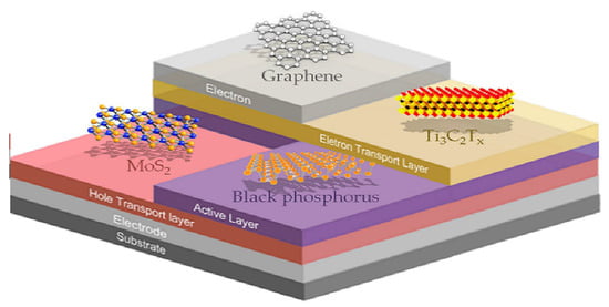
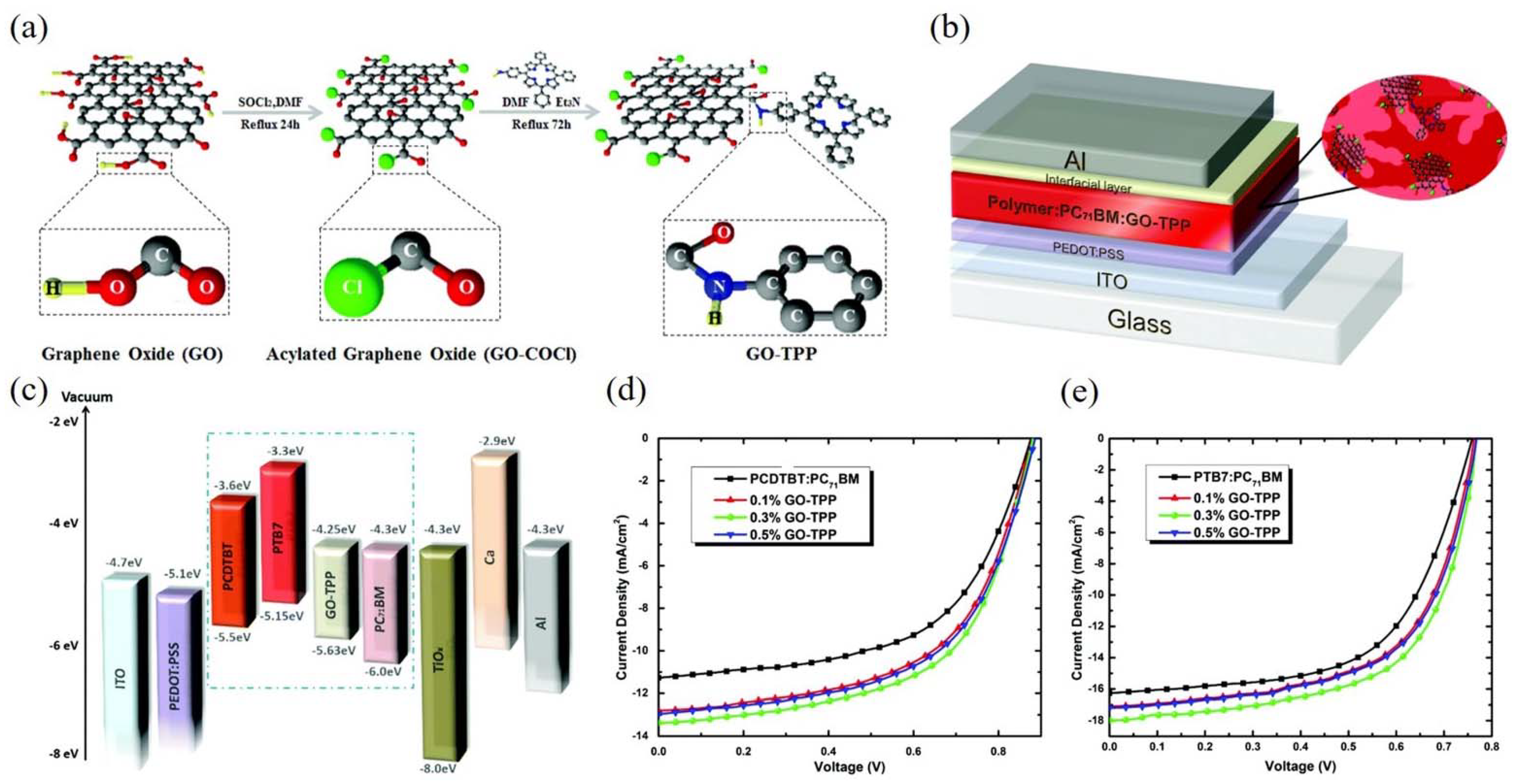
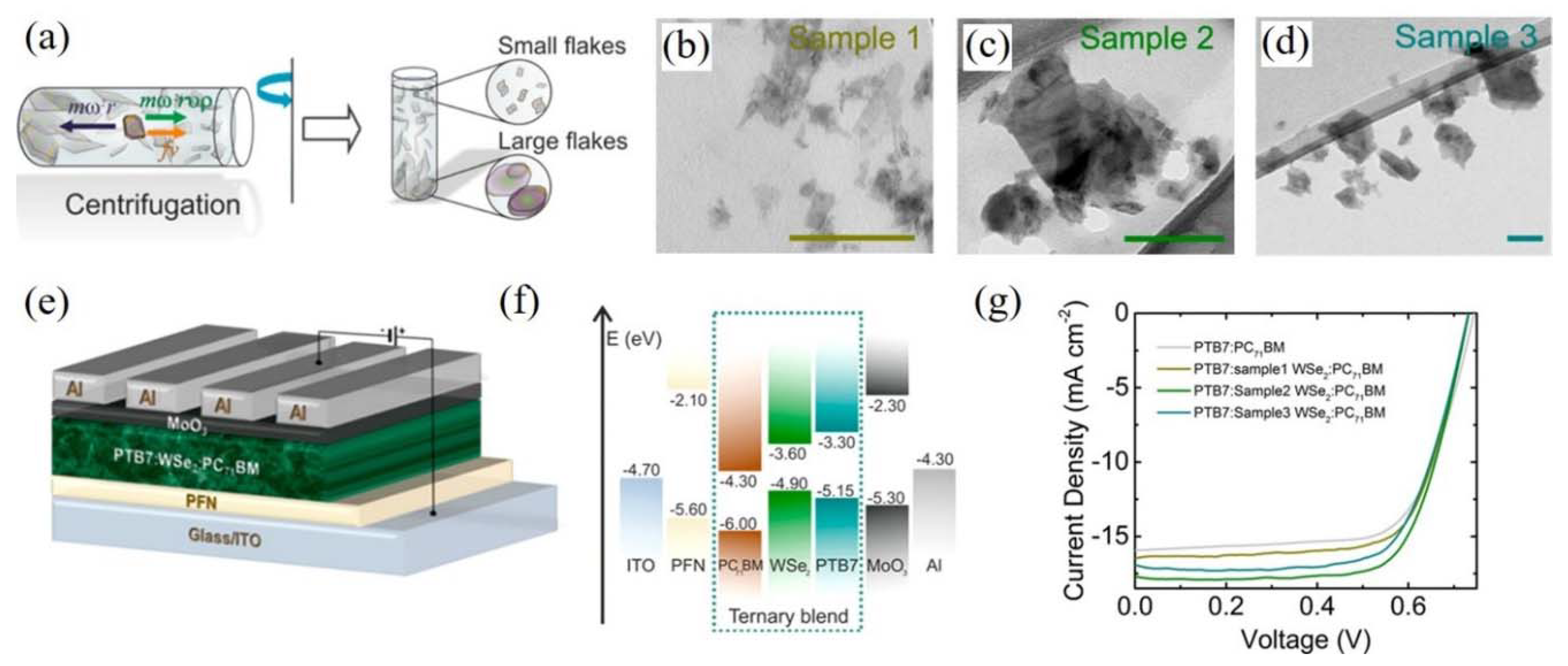
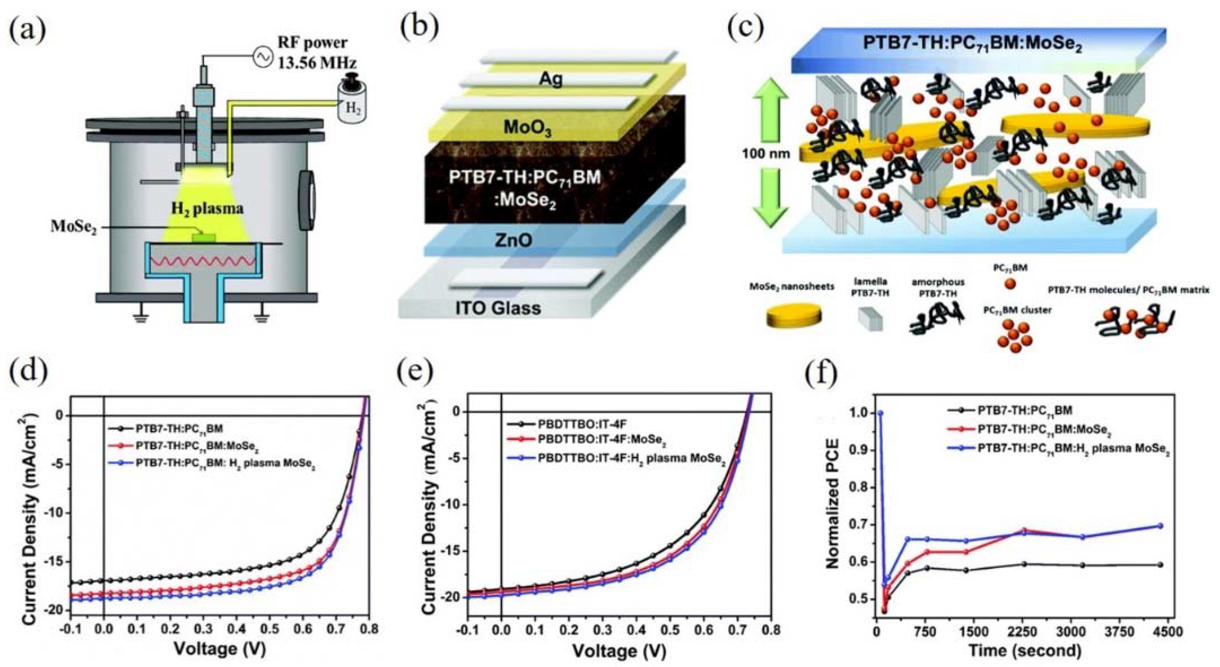
2. The Application of 2D Materials in the Active Layer


| NO. | Materials | Function | Device Structure | Jsc (mA/cm2) | Voc (V) | FF (%) | PCE (%) | PCE Enhancement (%) | Year | Ref. |
|---|---|---|---|---|---|---|---|---|---|---|
| 1 | TPP:GO | AL | ITO/PEDOT:PSS/PTB7:PC71BM:TPP:GO/MoO3/Au | 18.27 | 0.78 | 63 | 8.81 | 19.21 | 2015 | [63] |
| 2 | WSe2 | AL | Glass/ITO/PFN/PTB7:WSe2:PCBM/MoO3/Al | 17.84 | 0.73 | 72 | 9.45 | 16.67 | 2017 | [64] |
| 3 | MoSe2 | AL | ITO/ZnO/PBDTTBO:IT-4F:MoSe2/MoO3/Ag | 19.37 | 0.73 | 56 | 7.92 | 8.13 | 2019 | [65] |
| 4 | MoSe2 | AL | ITO/ZnO/PTB7-TH:PC71BM:MoSe2/MoO3/Ag | 18.69 | 0.78 | 70 | 10.44 | 15.74 | 2019 | [65] |
| 5 | BP | AL | ITO/PEDOT:PSS/PTB7-Th:PC71BM:BP/PFN/Al | 18.00 | 0.80 | 75 | 10.50 | 19.18 | 2018 | [67] |
| 6 | BP | AL | ITO/ZnO/J71:ITIC:BP/MoO3/Al | 16.6 | 0.95 | 60 | 9.41 | 11.89 | 2018 | [67] |
| 7 | BP | AL | ITO/ZnO/PTB7-Th:IEICO-4F:BP/MoO3/Ag | 23.44 | 0.71 | 70 | 12.2 | 12.96 | 2019 | [66] |
| 8 | Bi2O2S | AL | ITO/ZnO/PTB7:PC71BM:Bi2O2S/MoO3/Ag | 19.25 | 0.79 | 70 | 10.71 | 21.84 | 2019 | [70] |
| 9 | Bi2O2Se | AL | ITO/ZnO/PBDB-T:ITIC:Bi2O2Se/MoO3/Ag | 17.88 | 0.93 | 73 | 12.22 | 21.22 | 2020 | [76] |
| 10 | Bi2O2Se | AL | ITO/ZnO/PM6:Y6:Bi2O2Se/MoO3/Ag | 25.18 | 0.84 | 77 | 16.28 | 11.58 | 2020 | [76] |
| 11 | Ti3C2Tx | AL | ITO/PEDOT:PSS/PM6:Y6:Ti3C2Tx/PDINO/Al | 27.02 | 0.840 | 72 | 16.25 | 10.99 | 2021 | [79] |
| 12 | Ti3C2Tx | AL | ITO/PEDOT:PSS/PBDB-T:IT-M:Ti3C2Tx/PDINO/Al | 17.65 | 0.94 | 60 | 9.96 | 10.05 | 2021 | [79] |
| 13 | Ti3C2Tx | AL | ITO/PEDOT:PSS/PBDB-T:ITIC:Ti3C2Tx/PDINO/Al | 16.28 | 0.92 | 72 | 10.72 | 14.8 | 2021 | [79] |
3. The Application of 2D Materials in the HTL
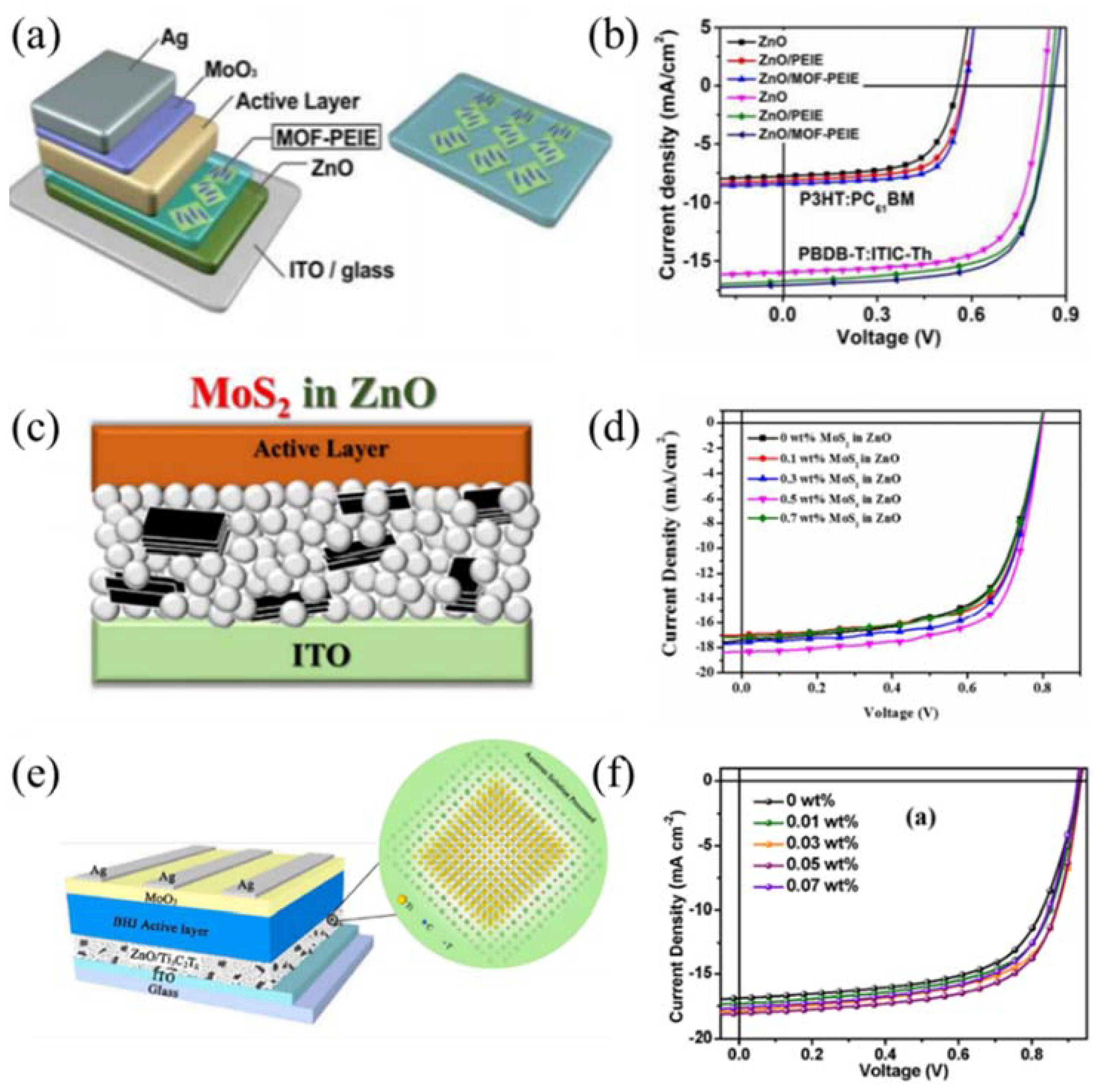
4. The Application of 2D Materials in the ETL
5. The Application of 2D Materials in the Electrodes
6. Conclusions
Funding
Institutional Review Board Statement
Informed Consent Statement
Data Availability Statement
Conflicts of Interest
References
- Ameri, T.; Khoram, P.; Min, J. Organic Ternary Solar Cells: A Review. Adv. Mater. 2013, 25, 4245–4266. [Google Scholar] [CrossRef]
- Liu, S.H.; You, P.; Li, J.H. Enhanced efficiency of polymer solar cells by adding a high-mobility conjugated polymer. Energy Environ. Sci. 2015, 8, 1463–1470. [Google Scholar] [CrossRef]
- Liu, S.H.; Jiang, R.B.; You, P. Au/Ag core-shell nanocuboids for high-efficiency organic solar cells with broadband plasmonic enhancement. Energy Environ. Sci. 2016, 9, 898–905. [Google Scholar] [CrossRef] [Green Version]
- Dao, V.D.; Vu, N.H.; Dang, H.L.T. Recent advances and challenges for water evaporation-induced electricity toward applications. Nano Energy 2021, 85, 105979. [Google Scholar] [CrossRef]
- Dao, V.D.; Vu, N.H.; Yun, S.N. Recent advances and challenges for solar-driven water evaporation system toward applications. Nano Energy 2020, 68, 104324. [Google Scholar] [CrossRef]
- Xie, L.; Song, W.; Ge, J.F. Recent progress of organic photovoltaics for indoor energy harvesting. Nano Energy 2021, 82, 105770. [Google Scholar] [CrossRef]
- Chen, Q.; Zhou, H.P.; Hong, Z.R. Planar Heterojunction Perovskite Solar Cells via Vapor-Assisted Solution Process. J. Am. Chem. Soc. 2014, 136, 622–625. [Google Scholar] [CrossRef] [PubMed]
- Liu, S.H.; Lin, S.H.; You, P. Black Phosphorus Quantum Dots Used for Boosting Light Harvesting in Organic Photovoltaics. Angew. Chem. Int. Ed. 2017, 56, 13717–13721. [Google Scholar] [CrossRef] [PubMed]
- Hossain, M.A.; Khoo, K.T.; Cui, X. Atomic layer deposition enabling higher efficiency solar cells: A review. Nano Mater. Sci. 2020, 2, 204–226. [Google Scholar] [CrossRef]
- Chen, S.S.; Liu, Y.H.; Zhang, L. A Wide-Bandgap Donor Polymer for Highly Efficient Non-Fullerene Organic Solar Cells with a Small Voltage Loss. J. Am. Chem. Soc. 2017, 139, 6298–6301. [Google Scholar] [CrossRef]
- Jiang, W.; Ye, L.; Li, X.G. Bay-linked perylene bisimides as promising non-fullerene acceptors for organic solar cells. Chem. Commun. 2014, 50, 1024–1026. [Google Scholar] [CrossRef]
- Liu, S.H.; Fu, Y.; Li, G.J. Conjugated Polymer for Voltage-Controlled Release of Molecules. Adv. Mater. 2017, 29, 1701733. [Google Scholar] [CrossRef] [Green Version]
- Zhang, A.D.; Li, C.; Yang, F. An Electron Acceptor with Porphyrin and Perylene Bisimides for Efficient Non-Fullerene Solar Cells. Angew. Chem. Int. Ed. 2017, 56, 2694–2698. [Google Scholar] [CrossRef]
- Fu, H.T.; Wang, Z.H.; Sun, Y.M. Polymer Donors for High-Performance Non-Fullerene Organic Solar Cells. Angew. Chem. Int. Ed. 2019, 58, 4442–4453. [Google Scholar] [CrossRef]
- Li, Z.K.; Jiang, K.; Yang, G.F. Donor polymer design enables efficient non-fullerene organic solar cells. Nat. Commun. 2016, 7, 13094. [Google Scholar] [CrossRef] [Green Version]
- Armin, A.; Li, W.; Sandberg, O.J. A History and Perspective of Non-Fullerene Electron Acceptors for Organic Solar Cells. Adv. Energy Mater. 2021, 11, 2003570. [Google Scholar] [CrossRef]
- Cui, Y.; Yao, H.F.; Hong, L. Organic photovoltaic cell with 17% efficiency and superior processability. Natl. Sci. Rev. 2020, 7, 1239–1246. [Google Scholar] [CrossRef] [PubMed]
- Li, C.; Zhou, J.D.; Song, J.L. Non-fullerene acceptors with branched side chains and improved molecular packing to exceed 18% efficiency in organic solar cells. Nat. Energy 2021, 6, 605–613. [Google Scholar] [CrossRef]
- Wu, J.N.; Li, G.W.; Fang, J. Random terpolymer based on thiophene-thiazolothiazole unit enabling efficient non-fullerene organic solar cells. Nat. Commun. 2020, 11, 4612. [Google Scholar] [CrossRef] [PubMed]
- Zhu, C.; Yuan, J.; Cai, F.F. Tuning the electron-deficient core of a non-fullerene acceptor to achieve over 17% efficiency in a single-junction organic solar cell. Energy Environ. Sci. 2020, 13, 2459–2466. [Google Scholar] [CrossRef]
- Lin, F.; Jiang, K.; Kaminsky, W. A Non-fullerene Acceptor with Enhanced Intermolecular π-Core Interaction for High-Performance Organic Solar Cells. J. Am. Chem. Soc. 2020, 142, 15246–15251. [Google Scholar] [CrossRef]
- Clarke, A.J.; Luke, J.; Meitzner, R. Non-fullerene acceptor photostability and its impact on organic solar cell lifetime. Cell Rep. Phys. Sci. 2021, 2, 100498. [Google Scholar] [CrossRef]
- Liu, S.H.; Li, C.Q.; Xu, X.M. Efficiency enhancement of organic photovoltaics by introducing high-mobility curved small-molecule semiconductors as additives. J. Mater. Chem. A 2019, 7, 12740–12750. [Google Scholar] [CrossRef]
- Yin, H.; Yan, C.Q.; Hu, H.L. Recent progress of all-polymer solar cells—From chemical structure and device physics to photovoltaic performance. Mater. Sci. Eng. R Rep. 2020, 140, 100542. [Google Scholar] [CrossRef]
- Cui, H.Q.; Song, W.; Fanady, B. Flexible ITO-free organic solar cells over 10% by employing drop-coated conductive PEDOT:PSS transparent anodes. Sci. China Chem. 2019, 62, 500–505. [Google Scholar] [CrossRef]
- Fan, X.; Xu, B.G.; Liu, S.H. Transfer-Printed PEDOT:PSS Electrodes Using Mild Acids for High Conductivity and Improved Stability with Application to Flexible Organic Solar Cells. ACS Appl. Mater. Interfaces 2016, 8, 14029–14036. [Google Scholar] [CrossRef]
- Yang, Q.; Yu, S.W.; Fu, P. Boosting Performance of Non-Fullerene Organic Solar Cells by 2D g-C3N4 Doped PEDOT:PSS. Adv. Funct. Mater. 2020, 30, 1910205. [Google Scholar] [CrossRef]
- Fernandez-Arteaga, Y.; Maldonado, J.L.; Nicasio-Collazo, J. Solution processable graphene derivative used in a bilayer anode with conductive PEDOT:PSS on the non-fullerene PBDB-T:ITIC based organic solar cells. Sol. Energy 2021, 225, 656–665. [Google Scholar] [CrossRef]
- Wang, J.; Peng, R.X.; Gao, J. Ti3C2TX/PEDOT:PSS Composite Interface Enables over 17% Efficiency Non-fullerene Organic Solar Cells. ACS Appl. Mater. Interfaces 2021, 13, 45789–45797. [Google Scholar] [CrossRef] [PubMed]
- Bao, Z.Y.; Liu, S.H.; Hou, Y.D. Hollow Au nanorattles for boosting the performance of organic photovoltaics. J. Mater. Chem. A 2019, 7, 26797–26803. [Google Scholar] [CrossRef]
- Hou, C.L.; Yu, H.Z. Modifying the nanostructures of PEDOT:PSS/Ti3C2TX composite hole transport layers for highly efficient polymer solar cells. J. Mater. Chem. C 2020, 8, 4169–4180. [Google Scholar] [CrossRef]
- Socol, M.; Preda, N. Hybrid Nanocomposite Thin Films for Photovoltaic Applications: A Review. Nanomaterials 2021, 11, 1117. [Google Scholar] [CrossRef] [PubMed]
- Eisner, F.; Seitkhan, A.; Han, Y. Solution-Processed In2O3/ZnO Heterojunction Electron Transport Layers for Efficient Organic Bulk Heterojunction and Inorganic Colloidal Quantum-Dot Solar Cells. Solar RRL 2018, 2, 1800076. [Google Scholar] [CrossRef] [Green Version]
- In, S.J.; Park, M.; Jung, J.W. Reduced interface energy loss in non-fullerene organic solar cells using room temperature-synthesized SnO2 quantum dots. J. Mater. Sci. Technol. 2020, 52, 12–19. [Google Scholar] [CrossRef]
- Liu, S.H.; Hou, Y.D.; Xie, W. Quantitative Determination of Contribution by Enhanced Local Electric Field, Antenna-Amplified Light Scattering, and Surface Energy Transfer to the Performance of Plasmonic Organic Solar Cells. Small 2018, 14, 1800870. [Google Scholar] [CrossRef]
- Yuan, J.B.; Zhang, X.L.; Sun, J.G. Hybrid Perovskite Quantum Dot/Non-Fullerene Molecule Solar Cells with Efficiency Over 15%. Adv. Funct. Mater. 2021, 31, 2101272. [Google Scholar] [CrossRef]
- Ahmed, E.; Ren, G.Q.; Kim, F.S. Design of New Electron Acceptor Materials for Organic Photovoltaics: Synthesis, Electron Transport, Photophysics, and Photovoltaic Properties of Oligothiophene-Functionalized Naphthalene Diimides. Chem. Mater. 2011, 23, 4563–4577. [Google Scholar] [CrossRef]
- Liu, S.H.; Zhang, Y.Y.; Lin, Y. Tailoring the structure and nitrogen content of nitrogen-doped carbon nanotubes by water-assisted growth. Carbon 2014, 69, 247–254. [Google Scholar] [CrossRef]
- Ren, G.Q.; Ahmed, E.; Jenekhe, S.A. Nanowires of oligothiophene-functionalized naphthalene diimides: Self assembly, morphology, and all-nanowire bulk heterojunction solar cells. J. Mater. Chem. 2012, 22, 24373–24379. [Google Scholar] [CrossRef]
- Wang, Y.F.; Jia, B.Y.; Qin, F. Semitransparent, non-fullerene and flexible all-plastic solar cells. Polymer 2016, 107, 108–112. [Google Scholar] [CrossRef]
- Zhao, F.G.; Deng, L.L.; Wang, K. Surface Modification of SnO2 via MAPbI3 Nanowires for a Highly Efficient Non-Fullerene Acceptor-Based Organic Solar Cell. ACS Appl. Mater. Interfaces 2020, 12, 5120–5127. [Google Scholar] [CrossRef] [PubMed]
- Butun, S.; Tongay, S.; Aydin, K. Enhanced Light Emission from Large-Area Monolayer MoS2 Using Plasmonic Nanodisc Arrays. Nano Lett. 2015, 15, 2700–2704. [Google Scholar] [CrossRef]
- Chen, Y.N.; Sun, Y.; Peng, J.J. Tailoring Organic Cation of 2D Air-Stable Organometal Halide Perovskites for Highly Efficient Planar Solar Cells. Adv. Energy Mater. 2017, 7, 1700162. [Google Scholar] [CrossRef]
- Fan, Q.P.; Zhu, Q.L.; Xu, Z. Chlorine substituted 2D-conjugated polymer for high-performance polymer solar cells with 13.1% efficiency via toluene processing. Nano Energy 2018, 48, 413–420. [Google Scholar]
- Ling, H.F.; Liu, S.H.; Zheng, Z.J. Organic Flexible Electronics. Small Methods 2018, 2, 1800070. [Google Scholar] [CrossRef]
- Ma, C.Q.; Shen, D.; Ng, T.W. 2D Perovskites with Short Interlayer Distance for High-Performance Solar Cell Application. Adv. Mater. 2018, 30, 1800710. [Google Scholar] [CrossRef]
- Das, S.; Pandey, D.; Thomas, J. The Role of Graphene and Other 2D Materials in Solar Photovoltaics. Adv. Mater. 2019, 31, 1802722. [Google Scholar] [CrossRef] [PubMed] [Green Version]
- Liu, Z.K.; Lau, S.P.; Yan, F. Functionalized graphene and other two-dimensional materials for photovoltaic devices: Device design and processing. Chem. Soc. Rev. 2015, 44, 5638–5679. [Google Scholar] [CrossRef]
- Zhou, H.L.; Wang, C.; Shaw, J.C. Large Area Growth and Electrical Properties of p-Type WSe2 Atomic Layers. Nano Lett. 2015, 15, 709–713. [Google Scholar] [CrossRef] [PubMed]
- Zhang, Y.; Chang, T.-R.; Zhou, B. Direct observation of the transition from indirect to direct bandgap in atomically thin epitaxial MoSe2. Nat. Nanotechnol. 2014, 9, 111–115. [Google Scholar] [CrossRef]
- Wu, M.; Zeng, X.C. Bismuth Oxychalcogenides: A New Class of Ferroelectric/Ferroelastic Materials with Ultra High Mobility. Nano Lett. 2017, 17, 6309–6314. [Google Scholar] [CrossRef] [PubMed]
- Meng, S.; Wang, J.; Shi, H. Distinct ultrafast carrier dynamics of α-In2Se3 and β-In2Se3: Contributions from band filling and bandgap renormalization. Phys. Chem. Chem. Phys. 2021, 23, 24313–24318. [Google Scholar] [CrossRef] [PubMed]
- Akinwande, D.; Petrone, N.; Hone, J. Two-dimensional flexible nanoelectronics. Nat. Commun. 2014, 5, 5678. [Google Scholar] [CrossRef]
- Nguyen, V.H.; Nguyen, B.S.; Hu, C.C. Novel Architecture Titanium Carbide (Ti3C2TX) MXene Cocatalysts toward Photocatalytic Hydrogen Production: A Mini-Review. Nanomaterials 2020, 10, 602. [Google Scholar] [CrossRef] [Green Version]
- Garg, R.; Dutta, N.K.; Choudhury, N.R. Work Function Engineering of Graphene. Nanomaterials 2014, 4, 267–300. [Google Scholar] [CrossRef] [Green Version]
- Suh, J.; Park, T.E.; Lin, D.Y. Doping against the Native Propensity of MoS2: Degenerate Hole Doping by Cation Substitution. Nano Lett. 2014, 14, 6976–6982. [Google Scholar] [CrossRef]
- Novoselov, K.S.; Geim, A.K.; Morozov, S.V. Electric field effect in atomically thin carbon films. Science 2004, 306, 666–669. [Google Scholar] [CrossRef] [Green Version]
- Eda, G.; Fanchini, G.; Chhowalla, M. Large-area ultrathin films of reduced graphene oxide as a transparent and flexible electronic material. Nat. Nanotechnol. 2008, 3, 270–274. [Google Scholar] [CrossRef]
- Eda, G.; Chhowalla, M. Chemically Derived Graphene Oxide: Towards Large-Area Thin-Film Electronics and Optoelectronics. Adv. Mater. 2010, 22, 2392–2415. [Google Scholar] [CrossRef]
- Konios, D.; Stylianakis, M.M.; Stratakis, E. Dispersion behaviour of graphene oxide and reduced graphene oxide. J. Colloid Interface Sci. 2014, 430, 108–112. [Google Scholar] [CrossRef] [PubMed]
- Huang, X.M.; Liu, L.Z.; Zhou, S. Physical properties and device applications of graphene oxide. Front. Phys. 2020, 15, 33301. [Google Scholar] [CrossRef] [Green Version]
- Cao, W.R.; Li, J.; Chen, H.Z. Transparent electrodes for organic optoelectronic devices: A review. J. Photonics Energy 2014, 4, 040990. [Google Scholar] [CrossRef]
- Stylianakis, M.M.; Konios, D.; Kakavelakis, G. Efficient ternary organic photovoltaics incorporating a graphene-based porphyrin molecule as a universal electron cascade material. Nanoscale 2015, 7, 17827–17835. [Google Scholar] [CrossRef] [PubMed]
- Kakavelakis, G.; Castillo, A.E.D.; Pellegrini, V. Size-Tuning of WSe2 Flakes for High Efficiency Inverted Organic Solar Cells. ACS Nano 2017, 11, 3517–3531. [Google Scholar] [CrossRef] [PubMed]
- Wang, H.C.; Lin, Y.C.; Chen, C.H. Hydrogen plasma-treated MoSe2 nanosheets enhance the efficiency and stability of organic photovoltaics. Nanoscale 2019, 11, 17460–17470. [Google Scholar] [CrossRef] [PubMed]
- Yang, W.T.; Ye, L.; Yao, F.F. Black phosphorus nanoflakes as morphology modifier for efficient fullerene-free organic solar cells with high fill-factor and better morphological stability. Nano Res. 2019, 12, 777–783. [Google Scholar] [CrossRef]
- Zhao, Y.; Chen, T.L.; Xiao, L.G. Facile integration of low-cost black phosphorus in solution-processed organic solar cells with improved fill factor and device efficiency. Nano Energy 2018, 53, 345–353. [Google Scholar] [CrossRef] [Green Version]
- Jun, G.H.; Jin, S.H.; Lee, B. Enhanced conduction and charge-selectivity by N-doped graphene flakes in the active layer of bulk-heterojunction organic solar cells. Energy Environ. Sci. 2013, 6, 3000–3006. [Google Scholar] [CrossRef]
- Fan, X.; Zhang, M.L.; Wang, X.D. Recent progress in organic-inorganic hybrid solar cells. J. Mater. Chem. A 2013, 1, 8694–8709. [Google Scholar] [CrossRef]
- Huang, C.W.; Yu, H.Z.; Chen, J.Y. Improved performance of polymer solar cells by doping with Bi2O2S nanocrystals. Sol. Energy Mater. Sol. Cells 2019, 200, 110030. [Google Scholar] [CrossRef]
- Wu, J.X.; Yuan, H.T.; Meng, M.M. High electron mobility and quantum oscillations in non-encapsulated ultrathin semiconducting Bi2O2Se. Nat. Nanotechnol. 2017, 12, 530–534. [Google Scholar] [CrossRef]
- Li, M.Q.; Dang, L.Y.; Wang, G.G. Bismuth Oxychalcogenide Nanosheet: Facile Synthesis, Characterization, and Photodetector Application. Adv. Mater. Technol. 2020, 5, 2000180. [Google Scholar] [CrossRef]
- Fatima, M.J.J.; Navaneeth, A.; Sindhu, S. Improved carrier mobility and bandgap tuning of zinc doped bismuth oxide. RSC Adv. 2015, 5, 2504–2510. [Google Scholar]
- Leontie, L.; Caraman, M.; Alexe, M. Structural and optical characteristics of bismuth oxide thin films. Surf. Sci. 2002, 507, 480–485. [Google Scholar] [CrossRef]
- Wu, J.X.; Qiu, C.G.; Fu, H.X. Low Residual Carrier Concentration and High Mobility in 2D Semiconducting Bi2O2Se. Nano Lett. 2019, 19, 197–202. [Google Scholar] [CrossRef]
- Huang, C.W.; Yu, H.Z. Two-Dimensional Bi2O2Se with High Mobility for High-Performance Polymer Solar Cells. ACS Appl. Mater. Interfaces 2020, 12, 19643–19654. [Google Scholar] [CrossRef]
- Naguib, M.; Kurtoglu, M.; Presser, V. Two-Dimensional Nanocrystals Produced by Exfoliation of Ti3AlC2. Adv. Mater. 2011, 23, 4248–4253. [Google Scholar] [CrossRef] [Green Version]
- Lei, J.C.; Zhang, X.; Zhou, Z. Recent advances in MXene: Preparation, properties, and applications. Front. Phys. 2015, 10, 276–286. [Google Scholar] [CrossRef]
- Zhao, Y.; Liu, X.J.; Jing, X. Addition of 2D Ti3C2TX to Enhance Photocurrent in Diodes for High-Efficiency Organic Solar Cells. Solar RRL 2021, 5, 2100127. [Google Scholar] [CrossRef]
- Gu, X.; Cui, W.; Li, H. A Solution-Processed Hole Extraction Layer Made from Ultrathin MoS2 Nanosheets for Efficient Organic Solar Cells. Adv. Energy Mater. 2013, 3, 1262–1268. [Google Scholar] [CrossRef]
- Gu, X.; Cui, W.; Song, T. Solution-Processed 2D Niobium Diselenide Nanosheets as Efficient Hole-Transport Layers in Organic Solar Cells. Chemsuschem 2014, 7, 416–420. [Google Scholar] [CrossRef] [PubMed]
- Koo, D.; Jung, S.; Oh, N.K. Improved charge transport via WSe2-mediated hole transporting layer toward efficient organic solar cells. Semicond. Sci. Technol. 2018, 33, 125020. [Google Scholar] [CrossRef]
- Lin, Y.B.; Adilbekova, B.; Firdaus, Y. 17% Efficient Organic Solar Cells Based on Liquid Exfoliated WS2 as a Replacement for PEDOT:PSS. Adv. Mater. 2019, 31, 1902965. [Google Scholar] [CrossRef] [PubMed]
- Yusoff, A.R.B.; Kim, D.; Schneider, F.K. Au-doped single layer graphene nanoribbons for a record-high efficiency ITO-free tandem polymer solar cell. Energy Environ. Sci. 2015, 8, 1523–1537. [Google Scholar] [CrossRef]
- Yu, J.C.; Jang, J.I.; Lee, B.R. Highly Efficient Polymer-Based Optoelectronic Devices Using PEDOT:PSS and a GO Composite Layer as a Hole Transport Layer. ACS Appl. Mater. Interfaces 2014, 6, 2067–2073. [Google Scholar] [CrossRef]
- Cheng, X.F.; Long, J.; Wu, R. Fluorinated Reduced Graphene Oxide as an Efficient Hole-Transport Layer for Efficient and Stable Polymer Solar Cells. ACS Omega 2017, 2, 2010–2016. [Google Scholar] [CrossRef] [PubMed] [Green Version]
- Cheng, J.Q.; Zhang, H.; Zhao, Y. Self-Assembled Quasi-3D Nanocomposite: A Novel p-Type Hole Transport Layer for High Performance Inverted Organic Solar Cells. Adv. Funct. Mater. 2018, 28, 1706403. [Google Scholar] [CrossRef]
- Zheng, X.; Zhang, H.J.; Yang, Q.L. Solution-processed Graphene-MoS2 heterostructure for efficient hole extraction in organic solar cells. Carbon 2019, 142, 156–163. [Google Scholar] [CrossRef]
- Wang, J.M.; Yu, H.Z.; Hou, C.L. Solution-Processable 2D α-In2Se3 as an Efficient Hole Transport Layer for High-Performance and Stable Polymer Solar Cells. Solar RRL 2020, 4, 1900428. [Google Scholar] [CrossRef]
- Wang, J.M.; Yu, H.Z.; Hou, C.L. Solution-Processable PEDOT:PSS:α-In2Se3 with Enhanced Conductivity as a Hole Transport Layer for High-Performance Polymer Solar Cells. ACS Appl. Mater. Interfaces 2020, 12, 26543–26554. [Google Scholar] [CrossRef] [PubMed]
- Huang, Y.J.; Chen, H.C.; Lin, H.K. Doping ZnO Electron Transport Layers with MoS2 Nanosheets Enhances the Efficiency of Polymer Solar Cells. ACS Appl. Mater. Interfaces 2018, 10, 20196–20204. [Google Scholar] [CrossRef]
- Chen, S.; Small, C.E.; Amb, C.M. Inverted Polymer Solar Cells with Reduced Interface Recombination. Adv. Energy Mater. 2012, 2, 1333–1337. [Google Scholar] [CrossRef]
- Lin, S.H.; Liu, S.H.; Yang, Z.B. Solution-Processable Ultrathin Black Phosphorus as an Effective Electron Transport Layer in Organic Photovoltaics. Adv. Funct. Mater. 2016, 26, 864–871. [Google Scholar] [CrossRef]
- Konios, D.; Kakavelakis, G.; Petridis, C. Highly efficient organic photovoltaic devices utilizing work-function tuned graphene oxide derivatives as the anode and cathode charge extraction layers. J. Mater. Chem. A 2016, 4, 1612–1623. [Google Scholar] [CrossRef]
- Zheng, D.; Huang, W.; Fan, P. Preparation of Reduced Graphene Oxide:ZnO Hybrid Cathode Interlayer Using In Situ Thermal Reduction/Annealing for Interconnecting Nanostructure and Its Effect on Organic Solar Cell. ACS Appl. Mater. Interfaces 2017, 9, 4898–4907. [Google Scholar] [CrossRef] [PubMed]
- Pan, F.; Sun, C.K.; Li, Y.F. Solution-processable n-doped graphene-containing cathode interfacial materials for high-performance organic solar cells. Energy Environ. Sci. 2019, 12, 3400–3411. [Google Scholar] [CrossRef]
- Xing, W.; Ye, P.; Lu, J. Tellurophene-based metal-organic framework nanosheets for high-performance organic solar cells. J. Power Sources 2018, 401, 13–19. [Google Scholar] [CrossRef]
- Hou, C.L.; Yu, H.Z. ZnO/Ti3C2TX monolayer electron transport layers with enhanced conductivity for highly efficient inverted polymer solar cells. Chem. Eng. J. 2021, 407, 127192. [Google Scholar] [CrossRef]
- Yusoff, A.; Lee, S.J.; Shneider, F.K. High-Performance Semitransparent Tandem Solar Cell of 8.02% Conversion Efficiency with Solution-Processed Graphene Mesh and Laminated Ag Nanowire Top Electrodes. Adv. Energy Mater. 2014, 4, 1301989. [Google Scholar] [CrossRef]
- Wang, B.Y.; Lee, E.S.; Oh, Y.J. A silver nanowire mesh overcoated protection layer with graphene oxide as a transparent electrode for flexible organic solar cells. RSC Adv. 2017, 7, 52914–52922. [Google Scholar] [CrossRef] [Green Version]
- Ricciardulli, A.G.; Yang, S.; Feng, X.L. Solution-Processable High-Quality Graphene for Organic Solar Cells. ACS Appl. Mater. Interfaces 2017, 9, 25412–25417. [Google Scholar] [CrossRef] [PubMed]
- Ricciardulli, A.G.; Yang, S.; Wetzelaer, G. Hybrid Silver Nanowire and Graphene-Based Solution-Processed Transparent Electrode for Organic Optoelectronics. Adv. Funct. Mater. 2018, 28, 1706010. [Google Scholar] [CrossRef]
- Jung, S.; Lee, J.; Seo, J. Development of Annealing-Free, Solution-Processable Inverted Organic Solar Cells with N-Doped Graphene Electrodes using Zinc Oxide Nanoparticles. Nano Lett. 2018, 18, 1337–1343. [Google Scholar] [CrossRef] [PubMed]
- Koo, D.; Jung, S.; Seo, J. Flexible Organic Solar Cells Over 15% Efficiency with Polyimide-Integrated Graphene Electrodes. Joule 2020, 4, 1021–1034. [Google Scholar] [CrossRef]
- Tang, H.H.; Feng, H.R.; Wang, H.K. Highly Conducting MXene-Silver Nanowire Transparent Electrodes for Flexible Organic Solar Cells. ACS Appl. Mater. Interfaces 2019, 11, 25330–25337. [Google Scholar] [CrossRef] [PubMed]
- Jinno, H.; Fukuda, K.; Xu, X. Stretchable and waterproof elastomer-coated organic photovoltaics for washable electronic textile applications. Nat. Energy 2017, 2, 780–785. [Google Scholar] [CrossRef]


| Materials | Bandgap (eV) | Carrier Mobility (cm2 V−1 s−1) | Ref. |
|---|---|---|---|
| WSe2 | 1.2–1.7 | 500 | [49] |
| MoSe2 | 1.5 | 50 | [50] |
| Bi2O2S | 1.27 | 16,000–26,000 | [51] |
| α-In2Se3 | 1.5–2.8 | 2.5 | [52] |
| BP | 0.3–2.0 | 1000 | [53] |
| Ti3C2Tx | 0–3.4 | 0.70 | [54] |
| Graphene | 0 | 1000 | [55] |
| MoS2 | 1.2–1.8 | 10–200 | [56] |
| NO. | Materials | Function | Device Structure | Jsc (mA/cm2) | Voc (V) | FF (%) | PCE (%) | PCE Enhancement (%) | Year | Ref. |
|---|---|---|---|---|---|---|---|---|---|---|
| 1 | MoS2 | HTL | ITO/ZnO/PTB7:PC71BM/MoS2/Ag | 15.90 | 0.72 | 71 | 8.11 | 7.56 | 2013 | [80] |
| 2 | NbSe2 | HTL | ITO/ZnO/PTB7:PC71BM/NbSe2/Ag | 16.04 | 0.72 | 70 | 8.10 | 7.42 | 2014 | [81] |
| 3 | WSe2 | HTL | ITO/PEDOT:PSS+WSe2/PTB7:PC71BM/Al | 16.60 | 0.78 | 66 | 8.5 | 19.71 | 2018 | [82] |
| 4 | WS2 | HTL | ITO/WS2/PBDB-T-2F:Y6:PC71BM/PFN-Br/Al | 26.00 | 0.84 | 78 | 17.00 | 6.25 | 2019 | [83] |
| 5 | WO3 | HTL | Glass/Au-doped single layer graphene nanoribbons/PEDOT:PSS+WO3/SMPV1:PC71BM/ZnO/PEDOT:PSS/PTTBDT-FTT:PC71BM/Ca/Al | 8.45 | 1.56 | 64 | 8.48 | 34.81 | 2015 | [84] |
| 6 | GO | HTL | ITO/PEDOT:PSS+GO/PTB7:PC71BM/Al | 16.42 | 0.76 | 65 | 8.21 | 16.61 | 2014 | [85] |
| 7 | F-rGO | HTL | ITO/F-rGO/PTB7-Th:PC71BM/PFN/Al | 16.89 | 0.78 | 65 | 8.60 | 8.86 | 2017 | [86] |
| 8 | L-GO +NiOx | HTL | ITO/ZnO/PBDB-T:IT-M/L-GO+NiOx/Ag | 18.07 | 0.92 | 73 | 12.13 | 21.17 | 2018 | [87] |
| 9 | GO+MoS2 | HTL | ITO/GO+MoS2/PEDOT:PSS/P3HT:PC71BM/Ca/Ag | 17.20 | 0.77 | 72 | 9.50 | 5.5 | 2019 | [88] |
| 10 | α-In2Se3 | HTL | ITO/α-In2Se3/PBDB-T:ITIC/Ca/Al | 16.69 | 0.88 | 65 | 9.58 | 0.8385 | 2019 | [89] |
| 11 | α-In2Se3 | HTL | ITO/PEDOT:PSS+α-In2Se3/PM6:Y6/PDINO/Al | 15.47 | 0.84 | 74 | 15.90 | 9.89 | 2020 | [90] |
| 12 | g-C3N4 | HTL | ITO/PEDOT:PSS+g-C3N4 | 26.71 | 0.84 | 73 | 16.38 | 7.13 | 2020 | [27] |
| NO. | Materials | Function | Device Structure | Jsc (mA/cm2) | Voc (V) | FF (%) | PCE (%) | PCE Enhancement (%) | Year | Ref. |
|---|---|---|---|---|---|---|---|---|---|---|
| 1 | BP | ETL | ITO/ZnO+BP/PTB7:PC71BM/MoO3/Ag | 18.78 | 0.72 | 61 | 8.25 | 11.9 | 2016 | [93] |
| 2 | GO | ETL | ITO/GO-Cl/PTB7:PC71BM/GO-Li/TiOx/Al | 19.59 | 0.78 | 61 | 9.14 | 23.68 | 2016 | [94] |
| 3 | rGO | ETL | ITO/IT-rGO/ZnO+IT-rGO/PTB7-Th:PC71BM/MoO3/Ag | 18.61 | 0.78 | 65 | 9.49 | 20.35 | 2017 | [95] |
| 4 | rGO | ETL | ITO/IT-rGO/ZnO+IT-rGO/PTB7:PC71BM/MoO3/Ag | 16.32 | 0.74 | 67 | 8.04 | 13.92 | 2017 | [95] |
| 5 | Graphene | ETL | ITO/ZnO+PDINO-G/PM6:Y6/MoO3/Ag | 25.12 | 0.82 | 76 | 15.70 | 15.6 | 2019 | [96] |
| 6 | MOF-PEIE | ETL | ITO/ZnO+MOF-PEIE/PBDB-T:ITIC-Th/MoO3/Ag | 17.09 | 0.86 | 71 | 10.39 | 14.80 | 2018 | [97] |
| 7 | MoS2 | ETL | ITO/ZnO+MoS2/PTB7-Th:PC71BM/MoO3/Ag | 18.40 | 0.80 | 69 | 10.10 | 14.77 | 2018 | [91] |
| 8 | Ti3C2Tx | ETL | ITO/ZnO+Ti3C2TX/PBDB-T:ITIC/MoO3/Ag | 18.63 | 0.93 | 70 | 12.20 | 15.53 | 2020 | [98] |
| 9 | Ti3C2Tx | ETL | ITO/ZnO+Ti3C2TX/PM6:Y6/MoO3/Ag | 26.38 | 0.83 | 75 | 16.51 | 10.13 | 2020 | [98] |
| NO. | Materials | Function | Device Structure | Jsc (mA/cm2) | Voc (V) | FF (%) | PCE (%) | PCE Enhancement (%) | Year | Ref. |
|---|---|---|---|---|---|---|---|---|---|---|
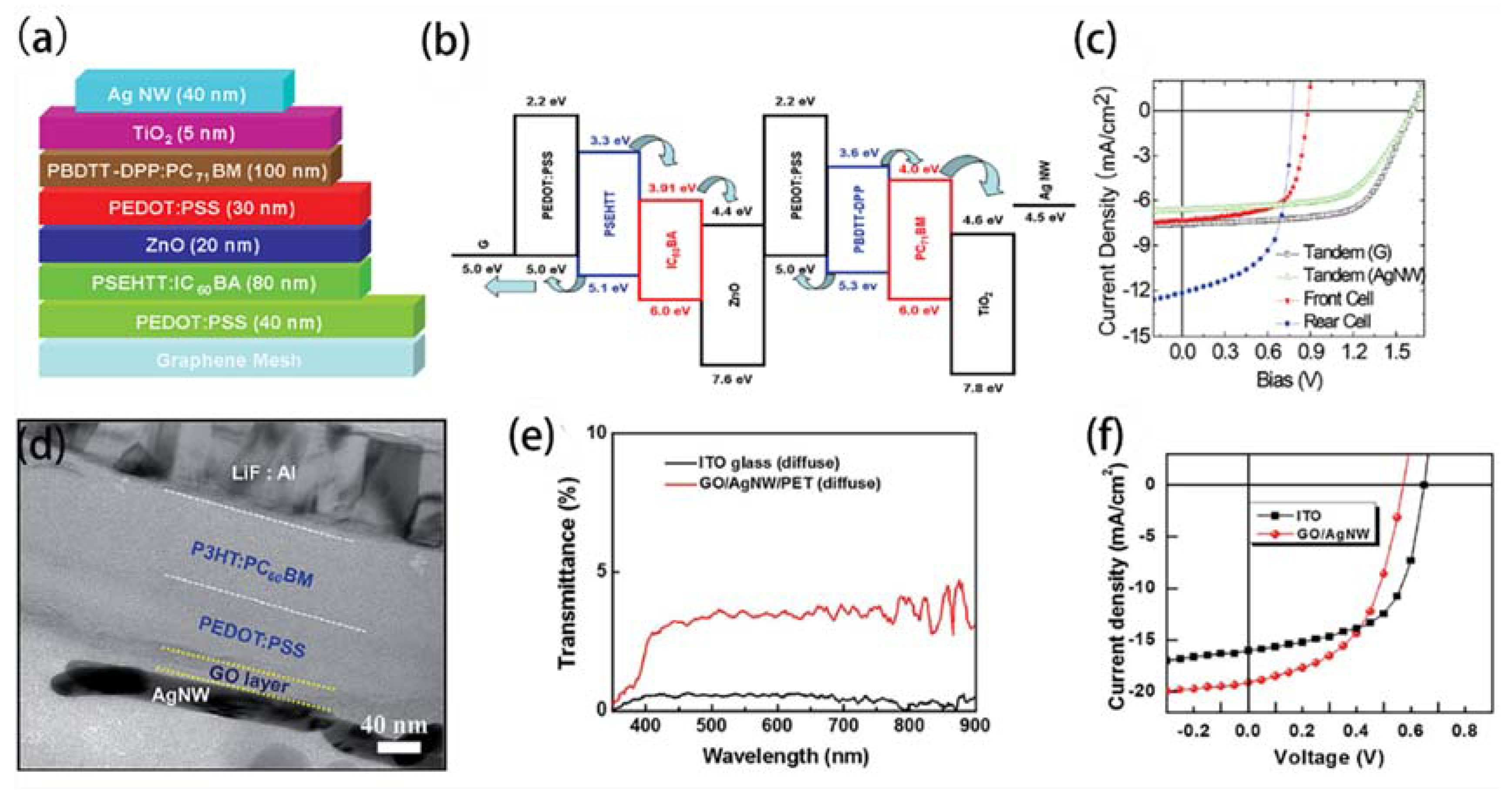
| 1 | Graphene | Anode | Graphene/PEDOT:PSS/WO3/SMPV1:PC71BM/ZnO/PEDOT:PSS/PTTBDT-FTT:PC71BM/Ca/Al | 8.45 | 1.56 | 64 | 8.48 | /4.95 | 2012 | [84] |
| 2 | rGO | Anode | rGO/PEDOT:PSS/PSEHTT:IC60BA/ZnO/PEDOT:PSS/PBDTT-DPP:PC71BM/TiO2/Ag NW | 7.62 | 1.62 | 64 | 8.02 | / | 2014 | [99] |
| 3 | GO@AgNWs | Anode | GO@AgNW/PEDOT:PSS/PTB7:PC70BM/LiF:Al | 19.84 | 0.68 | 57 | 7.66 | 5.36 | 2017 | [100] |
| 4 | EG | Anode | EG/PEDOT:PSS/PTB7:PC71BM/Ba/Al | 9.97 | 0.72 | 59.3 | 4.23 | /40.1 | 2017 | [101] |
| 5 | AgNWs-EG | Anode | AgNWs-EG/PEDOT:PSS/PTB7:PC71BM/Ba/Al | 15.5 | 0.73 | 58.3 | 6.57 | /7.1 | 2018 | [102] |
| 6 | GR/ZnO-NP | Cathode | GR/ZnO-NP/PTB7-Th:PC71BM/MoO3/Ag | 16.26 | 0.76 | 66.4 | 8.16 | /10.7 | 2018 | [103] |
| 7 | PI@GR | Anode | PI@GR/PEDOT:PSS/PM6:Y6/PDINO/Al | 25.8 | 0.84 | 70.2 | 15.2 | /3.2 | 2020 | [104] |
| 8 | MXene/AgNW-PUA | Anode | MXene/AgNW-PUA/PBDB-T:ITIC:PC71BM/PDINO/AI | 14.85 | 0.88 | 63 | 8.30 | /9.7 | 2019 | [105] |
Publisher’s Note: MDPI stays neutral with regard to jurisdictional claims in published maps and institutional affiliations. |
© 2021 by the authors. Licensee MDPI, Basel, Switzerland. This article is an open access article distributed under the terms and conditions of the Creative Commons Attribution (CC BY) license (https://creativecommons.org/licenses/by/4.0/).
Share and Cite
Wei, Z.; Chen, L.; Liu, K.; Liu, S.; Li, X.; Zhang, Q.; Shuai, J. Two-Dimensional Nanomaterials for Boosting the Performance of Organic Solar Cells. Coatings 2021, 11, 1530. https://doi.org/10.3390/coatings11121530
Wei Z, Chen L, Liu K, Liu S, Li X, Zhang Q, Shuai J. Two-Dimensional Nanomaterials for Boosting the Performance of Organic Solar Cells. Coatings. 2021; 11(12):1530. https://doi.org/10.3390/coatings11121530
Chicago/Turabian StyleWei, Zhenbang, Langkun Chen, Kunzhu Liu, Shenghua Liu, Xiangguo Li, Qian Zhang, and Jing Shuai. 2021. "Two-Dimensional Nanomaterials for Boosting the Performance of Organic Solar Cells" Coatings 11, no. 12: 1530. https://doi.org/10.3390/coatings11121530