1. Introduction
There are representative transition metal nitrides available, known as titanium nitride (TiN), chromium nitride (CrN), vanadium nitride (VN), and molybdenum nitride (MoN), that have excellent physicochemical properties, such as a low friction coefficient, corrosion resistance, and high-hardness [
1,
2,
3]. Particularly, molybdenum nitride (MoN) out of transition metal nitrides has been reported to be used in various applications on single- and poly-crystalline MoN coatings in, for example, an electromagnetic radiation detector, anode of Li-ion battery, and hydrogen generation reactor [
4,
5,
6,
7]. Because the application of coating film is dependent on the mechanical and electrical properties, it is generally important to manufacture coatings using a specific method. The reported manufacturing methods of MoN coating include reactive sputtering, DC sputtering, and pulse DC magnetron sputtering. Recently, a coating method using high-ionization plasma, such as high impulse plasma immersion magnetron sputtering (HiPIMS), has received attention [
8,
9,
10]. Particularly, inductively coupled plasma (ICP) generates plasma by permitting electricity to a round-coil antenna using RF power. The energy can be easily transferred to the charged particle of the internal antenna through the inductive-coil antenna. Moreover, unlike internal electrode or electron cyclotron resonance (ECR), it is widely highlighted because permitting the DC magnetic field and applications to treat relatively large plasma are unnecessary [
11]. Therefore, this study concentrated on inductively coupled plasma magnetron sputtering (ICPMS), which can generate high-density plasma in order to manufacture nano-crystalline MoN coating that increases the ICP power and has excellent physical properties. In this laboratory, many research papers have been published on the application of the deposition method using ICPMS and the change in properties due to the difference in plasma power [
12,
13]. However, there were no studies reported for the effect on the physical properties of MoN coatings manufactured by changing the ICP power. Therefore, this study was undertaken to investigate the effect on the crystal structure, microstructure, and mechanical/electrical properties of MoN coatings through ICP power changes.
2. Experimental Method
Si (100) substrate was used to manufacture MoN film in this experiment and dried after washing for 10 min both in acetone and ethyl alcohol using ultrasonic cleaner to remove impurities on the substrate surface. For more accurate comparisons of physical properties, this experiment maintained identical film formations, such as same chamber and process pressure. Mo target of 3″ diameter and 1/4″ depth (purity = 99.95%) was used as the starting material, and mass flow controller (MFC) was adopted for fixing 20 sccm of argon and 9 sccm of nitrogen (N2) in ultrapure gases to keep process circumstances. A distance between substrate and target was maintained of 60 mm at deposition, and the substrate was rotated in speed of approximately 10 rpm for uniform depositions. The chamber pressure was initially exhausted up to 3.5 × 10⁻³ Pa by rotary pump and ventilated again up to 3.5 × 10⁻⁵ Pa by turbo pump. Ion gauge and Baratron gauge were involved to measure the vacuum in this study. Argon plasma was generated prior to deposition and used for the secondary washing of target and substrate. The deposition times were identically performed during 30 min at 0, 50, 100, and 200 W, respectively. All films obtained from this experiment were processed by fixing substrate bias in −100 V. XRD (Multi-Purpose X-Ray Diffractometer, EMPYREAN, PANalytical, Almelo, Netherlands) was used for the crystal structure of MoN film and FE-SEM (Field-Emission Scanning Electron Microscope, S-3500N, Hitachi, Chiba, Japan), and AFM (Atomic Force Microscopy, Nanoscope IIIa, Digital Instruments, Veeco, NY, USA) for the surface microstructure and 3D morphology. In addition, the average value from 20 times test per sample in ESP (Enhanced Stiffness Procedure) mode was used by ultra nano-indenter (Helmut Fischer, Picodentor HM500, Helmut Fischer, Sindelfingen, Germany), which is the precise hardness tester for films to measure accurate mechanical–physical properties of coating films. With Semiconductor Characterization System (SUMMIT (11862B)/4200 SCS, Cascade/Keithley, Beaverton, OR, USA) and Van der Pauw method, repetitive tests more than 5 times per sample were completed to measure the electrical resistivity of MoN films.
3. Results and Discussion
To investigate the effect on the crystal structure, microstructure, such as surface and cross, 3D morphology, surface roughness, and mechanical–electrical properties according to the ICP power change, various MoN coatings were produced by changing the ICP power to 0, 50, 100 and 200 W in order.
3.1. Crystal Structure
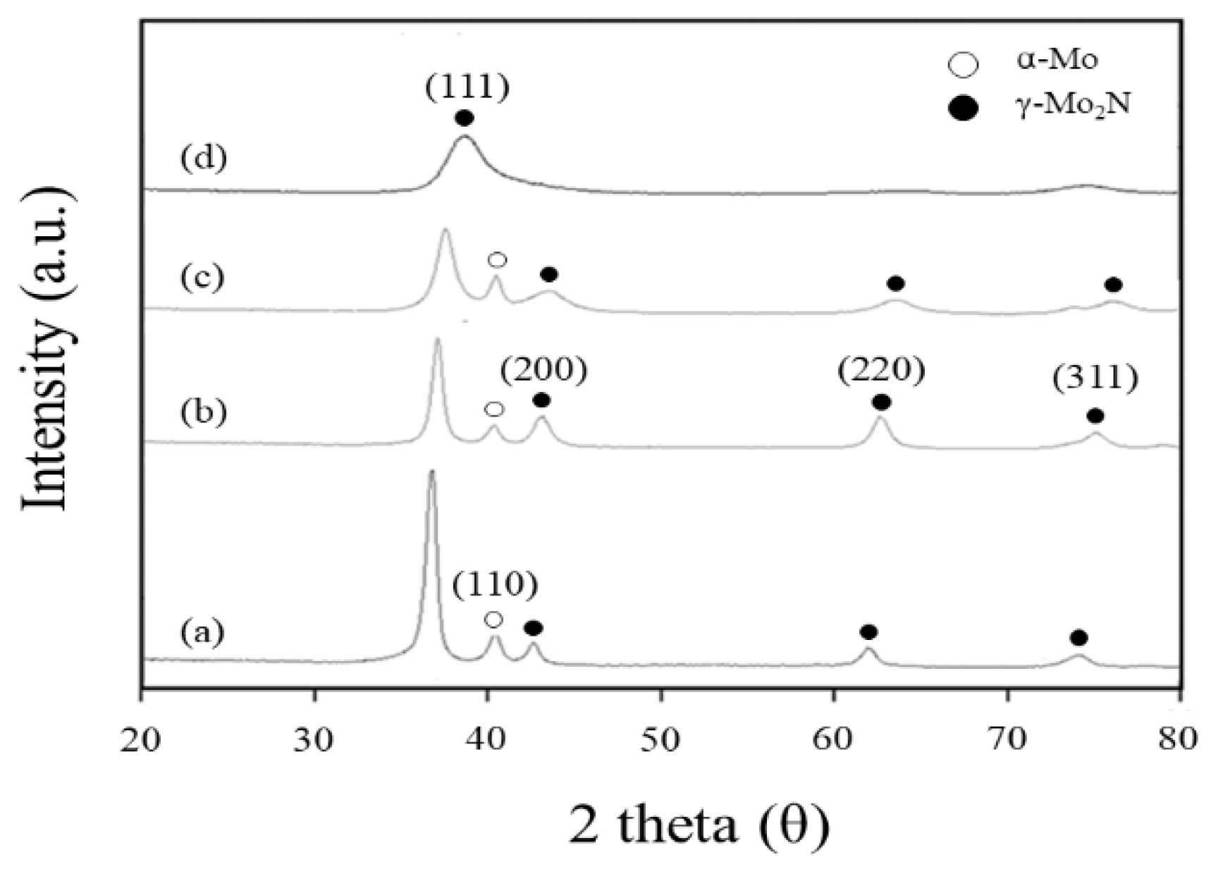
The crystal structure of γ-Mo
2N is stable at high temperatures. Its structure is a cubic shape in the type of NaCl-B1, so it could be explained as the cubic arrangement by which a nitrogen atom moves away from a Mo atom randomly occupying a half of the metal octahedron [
14]. An analysis of the X-ray diffraction was completed to identify the crystal structures and average grain sizes of the MoN coatings that were manufactured by different ICP powers.
Figure 1 indicates the results of this analysis. Peaks of (111), (200), (220), and (311) (JCPDS #25-1366) of the γ-Mo
2N and (110) of the α-Mo were observed from the MoN coatings that were produced in 0 W–100 W of ICP power. This means that the mixed shape of the γ-Mo
2N and α-Mo was determined from the MoN coatings manufactured in 0–100 W of ICP power, and the single shape was observed from the same coatings produced in 200 W of ICP power. The average crystalline grain size of the coatings can be estimated from the FWHM (Full Width at half Maximum) of the X-ray peaks.
The grain size is generally decreased by an increase of the half-value breadth of the diffraction peaks. Therefore, an average grain size of the MoN coating was calculated with the Scherrer equation.
Table 1 indicates 2θ variations of the (111) peak according to increasing ICP power. The average crystalline grain sizes of the MoN coatings that were manufactured in 0, 50, 100 and 200 W of ICP power were 10.4, 8.6, 7.4 and 6.7 nm, respectively. As a result, a consecutive decrease in the average sizes of the MoN coating could be concluded as the ICP power increases. This means that its size produced in 200 W of ICP power was diminished about 35% in contrast to 0 W of ICP power.
3.2. Residual Stress
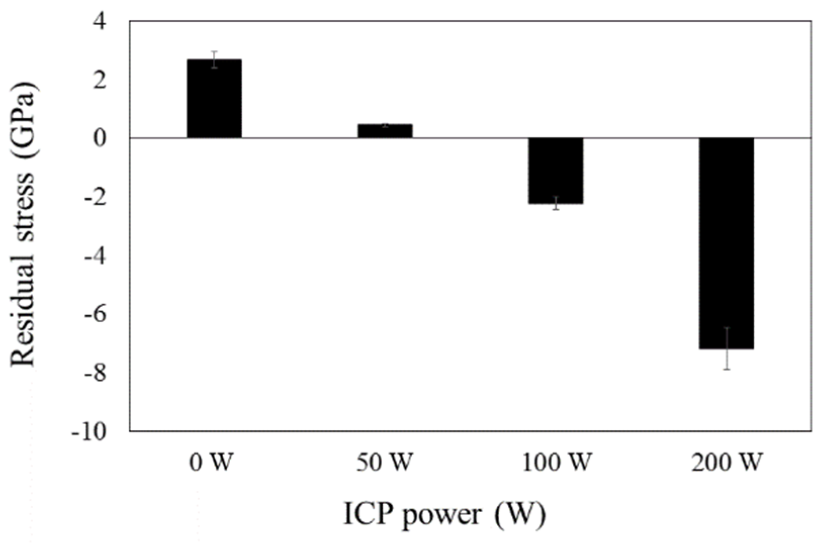
The results of the X-ray diffraction analysis were used to estimate the residual stress of the coatings in this study. In general, a 2θ value of the X-ray diffraction peak of the coatings presents higher or lower angle shifts from the standard peak. Therefore, any residual stresses (compressive or tensile stresses) could exist in the coating films. If a 2θ value of the X-ray diffraction peak shifts in a higher angle, it could be explained that the compressive stress had been applied to decrease the distance spacing. Moreover, an increase in the distance spacing represents the tensile stress.
Table 2 shows the specific results of the distance spacing (d) and lattice constant (a) of the coating films, which are determined by the (111) peak. As known from
Table 1, a 2θ value of the (111) peak of the MoN coatings was shifted to a higher angle according to the increasing ICP power. This indicates the consecutive increase of the compressive stresses in the coatings as the ICP power increases. The actual values of the residual stress were estimated from the strain values using the following equation to quantify the residual stress that existed in the coatings [
15].
From the above equation, ∆d/d is a strain value calculated from the distance spacing of the MoN (111) peak. A multiplication of the elastic modulus into the strain value was used to estimate the residual stresses, and
Figure 2 includes the result [
15]. The residual stresses from the MoN coatings manufactured by 0 W and 50 W of the ICP power were +2.66 GPa and +0.44 GPa, indicating the tensile stress effected to the corresponding films. However, the residual stresses from the MoN coatings by 100 and 200 W were −2.33 and −7.19 GPa, showing the compressive stress effected. Besides, the residual stress was decreased from a +2.66 GPa maximum to −7.19 GPa minimum according to the increasing ICP power. This means that the residual stress was converted from the tensile stress to the compressive stress by its power increases.
3.3. Microstructure
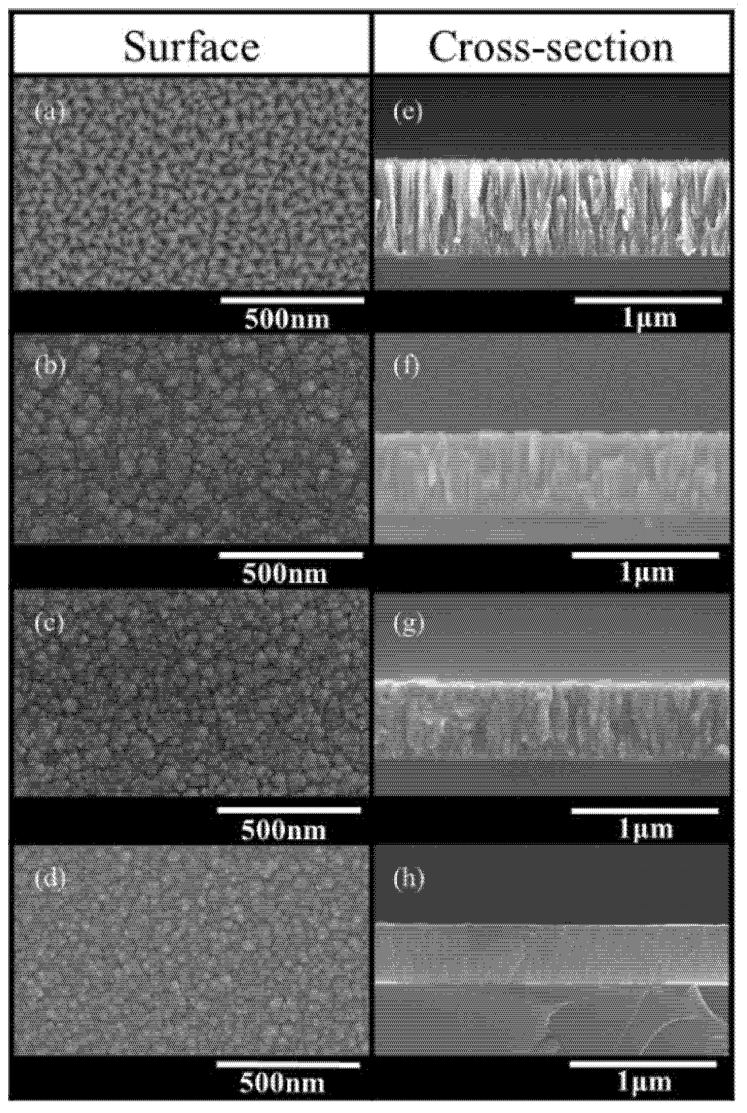
FE-SEM was used for observing the microstructure changes in the MoN coatings according to the ICP power.
Figure 3 presents its surface and cross photos. Rough spinous process particles were shown on the surface of the MoN coatings produced by 0 W of ICP power, and the porous columnar structure having a clear grain boundary from substrate to film surface was observed on the cross. In the case of the MoN coating films manufactured by 50 and 100 W of ICP power, round particles that resembled broccoli were shown on the surface, but the decrease in the columnar-boundary microstructure was examined on the cross due to pore reductions and its densifications. Particularly, the MoN coatings produced by 200 W of ICP power obtained small round particles on the surface and monitored coatings of the dense structure on the cross.
The thickness of the coatings produced with the ICP power of 0, 50, and 200 W were 685, 572, and 457 nm, respectively, and the thickness of the coating showed a tendency to decrease as the ICP power increased. The causes of the decrease in the coating thickness according to the increase in the ICP power can be explained as below: (1) the densification of the microstructure due to the reduction in the average particle size and pores; (2) the resputtering effect according to the generation of high-energy particles by the ionization/dissociation reaction according to the generation of high-density ICP [
16].
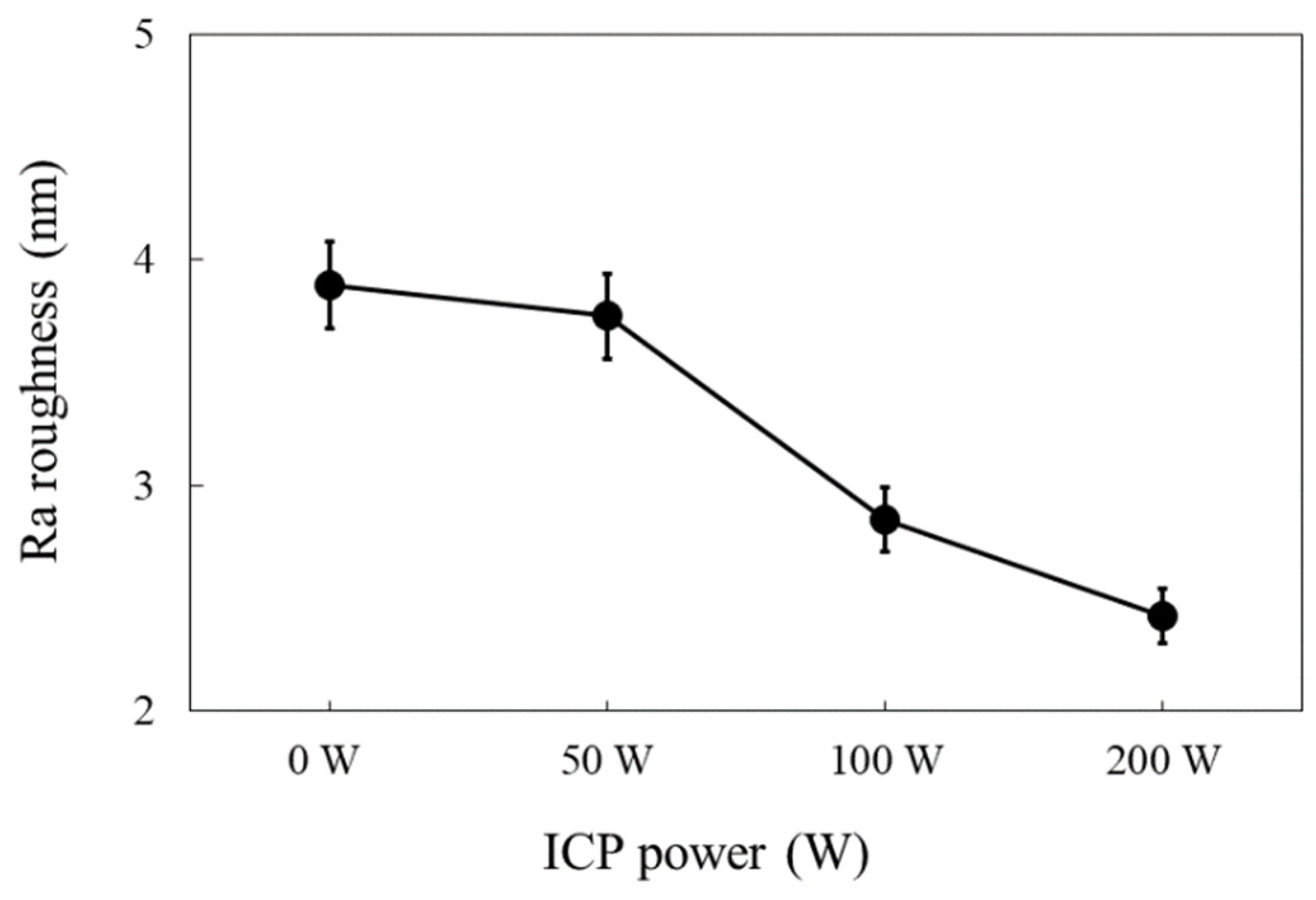
3.4. 3D Morphology and Surface Roughness
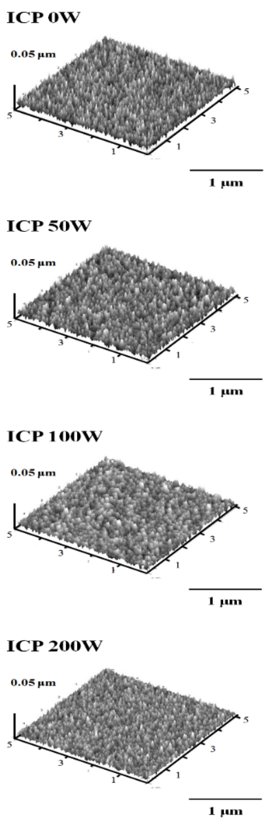
Figure 4 and
Figure 5 represent the result followed by non-contact AFM analysis to determine the effects on the 3D morphology and surface roughness of the MoN coating by the ICP power. Compared to the result of the surface roughness (Ra) of the MoN coating, the ICP power obtained consistent decreases in the surface roughness. The 3D morphology had a much flatter MoN coating by 200 W than 0 W of ICP power. The surface roughness values of the MoN coating by 0 and 200 W were 3.9 and 2.4 nm, indicating the maximum 38% decrease in accordance with the increasing ICP power. The reasons of surface flattening and decreases of surface roughness for the MoN coatings according to the ICP power variations are identical to the adatom movements and nucleation density increase of the ions, which were accelerated by upsurging ion energy by high-density plasma generations. Further, this laboratory has recently reported in a research paper that the generation of high-density and ionization plasma had a close relationship with the decreasing surface roughness of coating films. For example, for HfN, which is one of the transition metal nitrides and has a similar crystal structure, the surface roughness of the coating could be decreased by a maximum of approximately 52% by using high-density plasma [
17].
3.5. Nano-Indentation Hardness and Elastic Modulus
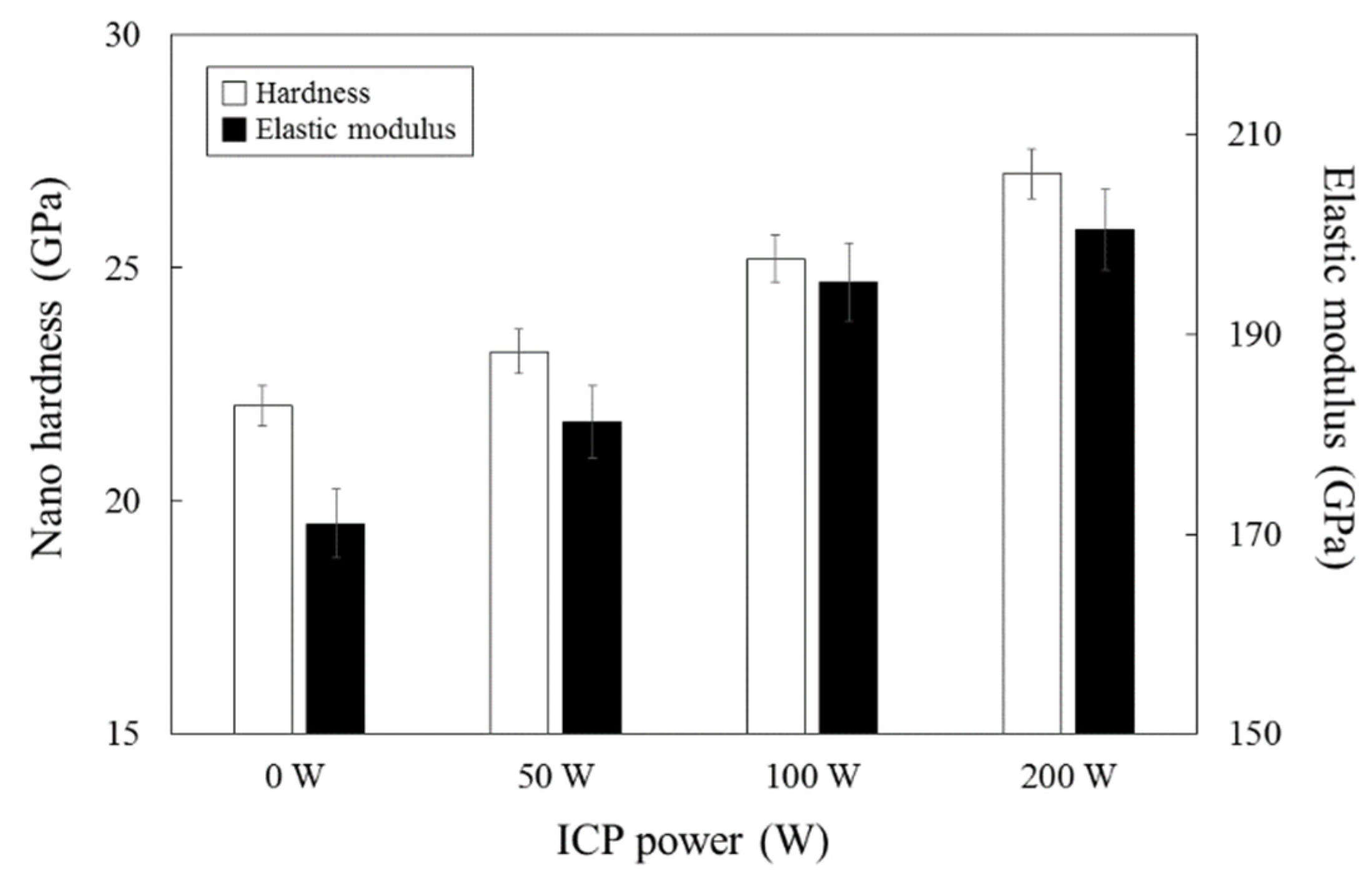
Figure 6 exhibits the analytical results for the nano-indentation hardness and elastic modulus followed by measuring the mechanical hardness of the MoN coatings 20 times per sample as a unit of 1 micrometer with the nano-indentation system. Its measurement was performed by the enhanced stiffness procedure (ESP) mode and was tested in a maximum 1.8 mN of load for 300 s. Notably, the test locations were averaged at the point of 1/10 of the total film depth to exclude indentation size effects that might increase the actual hardness as shallow indentation depth. The nano-indentation hardness and elastic resistivity of the MoN coatings can be identified from the above figure, showing a proportional increase according to increasing ICP power. Even the nano-indentation hardness and elastic resistivity of the MoN coatings by 0 W of ICP power were 22.1 GPa and 171.1 GPa, respectively; the mechanical properties manufactured by 200 W of ICP power could definitely be improved about 23%, as shown with 27.1 GPa and 200.5 GPa for both. In general, the mechanical property of coating films is determined by complicated elements, such as microstructure and residual stress. Therefore, its property could be improved by micronized average grain, microstructure densification, and the change of residual stress from tensile stress to compressive stress in accordance with increasing ICP power.
3.6. Electrical Resistivity
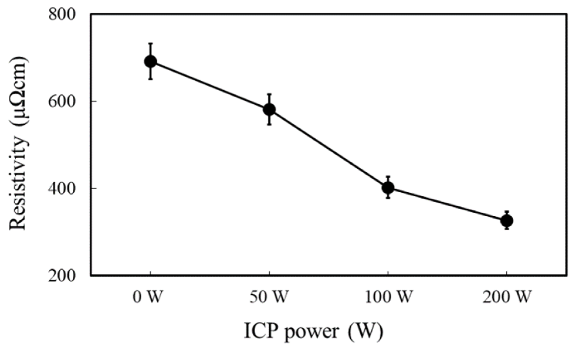
For the measurements of the electrical resistivity of the MoN coatings as the ICP power increases, the analysis was completed by a semiconductor tester, and the result is shown in
Figure 7. There are two types of methods available to test the resistivity of semiconductor materials: the four-point probe method and the
Van der Pauw method. As a contact interval is not important for testing electrical resistance and it is useful to test very tiny samples, this study adopted the
Van der Pauw method, which can measure the voltage by the current with four points of probes at a consistent depth of the samples. The obtained resistivity of the MoN coating showed a decrease by increasing the ICP power. The electrical resistivity values of the MoN coating manufactured by 0 W and 200 W of ICP power were 691.6 and 325.9 μΩcm, indicating a decrease of about 53% by rising ICP power. The reasons for this resistivity decrease include the impurity within the coating films, a decrease in the average grain size, and microstructure densification. As known from the results of X-ray diffraction, only a single γ-Mo
2N phase received the lowest electrical resistivity from the coatings by 200 W of ICP power.
4. Conclusions
In this study, coatings of nano granular MoN were manufactured by increasing the ICP power to 0, 50, 100 and 200 W. An increase in the ICP power resulted not only in the changes of structural properties, such as the crystal structure, surface, and cross microstructure of coatings, but also in effects on mechanical and electrical properties, such as nano-indentation hardness, elastic modulus, and electrical resistivity. The crystal structure of the Mo and γ-Mo2N in the MoN manufactured by 0, 50 and 100 W showed a mixed phase but single γ-Mo2N phase by 200 W of ICP power. As a result of calculating the residual stress, the values of the tensile stress were +2.66 and +0.44 GPa for the MoN coating by 0 W and 50 W of ICP power. In addition, the values of the compressive stress were −2.33 and −7.19 GPa for the MoN coating by 100 and 200 W of ICP power. This means that an increase in the ICP power contributed to a change in the residual stress from tensile to compressive in the MoN coatings. In the microstructure, a spiked surface and columnar structured cross including many pores were observed from the MoN coating manufactured by 0 W of ICP power. Moreover, the MoN coating by 200 W of ICP power showed the round and smooth surface and the refined cross. The surface roughness (Ra) was decreased from 3.9 nm of the MoN coating by 0 W to 2.4 nm by 200 W of the ICP power. The nano-indentation hardness and elastic modulus of the MoN coating by 0 W were 22.0 GPa and 171.1 GPa, respectively, but were 22.0 and 171.1 GPa for the film by 200 W of the ICP power as it improved its mechanical property by about 23%. From the result of the electrical property, the electrical resistivity was decreased by approximately 53% from 691.6 μΩcm in the MoN coating by 0 W to 325.9 μΩcm by 200 W of ICP power.


