1. Introduction
Zinc oxide (ZnO) is an abundant raw material. It is a II-VI group wide-bandgap oxide semiconductor and exhibits superior physical properties such as chemical and thermal stability, biocompatibility, high radiation resistance, good optical transparency in the visible spectral range, high quantum yield, a wide range of electrical resistivity and high voltage-current nonlinearity [
1,
2,
3,
4,
5]. It is a promising semiconductor material for electronic and optoelectronic applications, especially in excitonic devices [
6]. Pristine ZnO crystals exhibit n-type conductivity due to a deviation from stoichiometry and the presence of intrinsic donors (point defects) of oxygen vacancies and zinc interstitials [
7,
8].
It has been demonstrated that the electrical characteristics and optical parameters of ZnO thin films can be improved by doping with extrinsic dopants such as group II, III and IV elements [
9,
10]. Particularly, the group III elements, such as boron (B), aluminum (Al), gallium (Ga) and indium (In), are the most considerable dopants utilized as extrinsic donors for promotion of the electrical and optoelectrical characteristics of n-type ZnO thin films [
11,
12]. It is well agreed that ZnO thin films doped with B, Al, Ga and In ions become more conductive, because one excess electron is produced in those thin films [
13]. A number of studies on the physical properties of Al-doped ZnO (ZnO:Al) thin films prepared by various techniques have been reported due to their non-toxicity, low-cost, simple fabrication, abundance of the raw materials and competitive optoelectronic properties with indium tin oxide (ITO) thin films [
14,
15,
16]. The substitution of two kinds of extrinsic group III dopants (namely dual-donors simultaneously co-doping) is considered an effective approach to enhance the electrical characteristics and optical parameters of ZnO thin films [
17,
18,
19]. The ionic radii of B
3+ (0.23 Å) and Al
3+ (0.51 Å) are smaller than the ionic radius of Zn
2+ (0.74 Å), allowing easy substitution of B
3+ and Al
3+ for Zn
2+ and decrement of the lattice parameters, which leads to volume shrinkage of the unit cells [
4,
20].
The influence of Al and B co-doping on the physical properties of ZnO thin films has been little discussed, for few reports on them have been published. In 2010, Kang et al. first reported the optical and electrical properties of Al-B co-doped ZnO thin films deposited by DC magnetron sputtering and concluded that Al-B co-doped ZnO thin films are good candidates for optical device applications [
21]. Im et al. prepared Al and B co-doped ZnO thin films via RF magnetron sputtering and found that substitution of Al and B for Zn of up to 3 wt.% could increase the optical bandgap energy and electron concentration of ZnO thin films [
22]. Nevertheless, they did not present a clear and detailed discussion of why the optical parameters were adjusted and electrical characteristics were improved. Moreover, there is no report on Al-B co-doping ZnO semiconductor thin films prepared via solution-based processes. Sol-gel spin-coating is a simple process, has low equipment and raw material costs, and allows easy adjustment of the composition. It provides a solution deposition route for large-area functional oxide thin films with high efficiency in technological production. In the present study, the microstructural features, electrical characteristics and optical properties of ZnO, Al-doped ZnO (ZnO:Al) and Al-B co-doped ZnO (ZnO:Al-B) semiconductor thin films were investigated in detail and compared. In addition, the optical parameters, including the optical bandgap, Urbach energy, extinction coefficient and refractive index, are reported in this study.
3. Results and Discussion
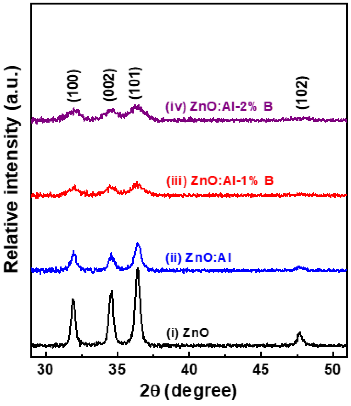
The crystal structure and crystallinity of the ZnO-based thin films were analyzed by XRD examination. The XRD patterns of sol-gel derived undoped and extrinsically doped ZnO thin films, shown in
Figure 1, indicated that the as-prepared oxide thin films were polycrystalline in structure. Four diffraction peaks were identified by comparison with ICDD (International Center for Diffraction Data) data No. 00-005-0664 and corresponded to the (100), (002), (101) and (102) crystallographic planes of ZnO crystals, confirming the growth of the hexagonal wurtzite phase. In addition, neither metallic nor other oxide characteristic peaks were observed in the XRD patterns, suggesting the formation of single-phase oxide thin films. It was observed that the diffraction peaks of singly doped and co-doped samples were broader than those of the undoped sample, indicating that the extrinsically doped ZnO thin films had finer microstructures than that of the undoped ZnO thin film. In addition, the diffraction signals significantly decreased with increased extrinsic doping levels, especially the characteristic peak of the (102) plane. This finding revealed that the crystallinity of the extrinsically doped thin films had deteriorated.
According to standard XRD data, the XRD relative intensity of diffraction peaks (I
(101)/I
(100)+(002)+(101)) of ZnO bulk crystals is 0.497.
Table 1 lists the calculated results of the XRD relative intensities of I
(101)/I
(100)+(002)+(101) for the four ZnO-based thin film samples. The XRD relative intensities of the four samples were obviously smaller than that of the ZnO bulk sample, and the relative intensities of the films were reduced with increased extrinsic dopant content because extrinsic doping led to random growth of crystallites. The incorporation of extrinsic dopants into ZnO lattices likely caused changes in the lattice parameters c and a of the hexagonal wurtzite. According to the ICDD database, the c/a ratio of ZnO bulk is 1.602; the determined c/a ratios for ZnO, ZnO:Al, ZnO:Al-1% B and ZnO:Al-2% B thin films were 1.600, 1.604, 1.613 and 1.600, respectively.
The average crystallite sizes of the as-prepared oxide film samples were estimated by Scherrer’s formula from the X-ray wavelength, peak broadening (full widths at half-maximum) and Bragg diffraction angles of the three major diffraction peaks, including (100), (002) and (101), which were acquired from the XRD data. The estimated results are summarized in
Table 1. The undoped ZnO thin film had an average crystallite size of 23.08 nm. The average crystallite sizes of Al doped, Al-1% B and Al-2% B co-doped ZnO thin films were 19.88 nm, 12.76, nm and 10.93 nm, respectively. The crystallite size decreased with increasing extrinsic doping content. It was recognized that the as-prepared ZnO-based thin films comprised nanocrystallites and the two ZnO:Al-B samples had finer average crystallite sizes than those of the ZnO and ZnO:Al samples because the extrinsic doping caused lattice distortion that apparently led to inhibition of the nanocrystal growth. Fujihara et al. reported that Al doping can reduce the concentration of zinc interstitials, resulting in the suppression of grain growth of ZnO thin films because of decreased diffusivity [
23].
The cross-sectional FE-SEM micrographs of the obtained ZnO-based thin films on Corning 1737 glass are shown in
Figure 2. These micrographs revealed that the oxide films possessed obviously granular microstructures, uniform particle size distributions and uniform thickness. It can also be seen in the figure that nano-sized pores were retained inside the ZnO-based thin films. These defects can be attributed to thermal decomposition of precursors and residual organic compounds in the sol-gel films [
14]. Moreover, it was significantly observed that the particle size of the obtained thin film samples was strongly affected by the extrinsic doping content and that the Al-2% B co-doped ZnO thin film had the smallest particles. The thicknesses of the films were determined from the corresponding cross-sectional FE-SEM micrographs. According to cross-sectional observation, the mean thicknesses of the ZnO, ZnO:Al and ZnO:Al-B thin films were 115 nm, 75 nm and 87 to 88 nm, respectively, as presented in
Table 1. The differences in thickness among the four ZnO-based sol-gel films can be attributed to changes in the viscosity of the coating solutions after Al and B metallic salts were added.
The surface morphology and root-mean-square (RMS) roughness of the films were studied by SPM. Three-dimensional (3D) SPM images acquired from the free surfaces of glass/thin film samples are presented in
Figure 3, illustrating a significantly granular configuration without the presence of cracks or porosity. These dense surfaces consisted of close-packed nano-sized particles. In addition, decreases in the particle size due to Al-doping and Al-B co-doping were observed from the SPM images. The average particle sizes of the ZnO, ZnO:Al, ZnO:Al-1% B and ZnO:Al-2% B thin films, estimated from the corresponding two-dimensional (2D) SPM images, were 37.19, 28.78, 28.19 and 23.65 nm, respectively (see
Figure S1 and
Table 1). The tendency of the microstructural features to vary with the extrinsic doping content of the obtained ZnO-based thin films was consistent with the XRD analysis and FE-SEM observation.
Table 1 lists the surface RMS roughness values of the four ZnO-based thin film samples. These results revealed that RMS roughness decreased with increases in extrinsic dopants due to reduction of the particle size.
The expected elements in the obtained ZnO-based thin films were confirmed by a broad scan survey of XPS analysis (no shown). The narrow scan XPS examinations identified the chemical bonding states of Zn and O in the obtained thin film samples.
Figure 4a shows the core level XPS spectra of Zn 2p. The four ZnO-based thin films exhibited a similar Zn 2p XPS spectrum, and the binding energies of the peaks located at 1020.0 eV and 1043.2 eV for the pristine ZnO thin film sample corresponded to the electronic states of Zn 2p
3/2 and Zn 2p
1/2, respectively (spectrum (i)) [
24]. The electronic state of Zn 2p
3/2 is related to Zn
2+ ions in the ZnO lattice and dependent on Zn–O and Zn–Zn bonds [
25]. Moreover, the binding energies of the two Zn 2p peaks for the singly doped and co-doped samples showed slight shifts of 0.2 eV toward the higher binding energy region due to changes in the strength of the metal–oxygen bond energy resulting from the incorporation of Al and Al-B dopants in the ZnO crystals.
The examined XPS spectra of O 1s were broad and significantly asymmetric in the high binding energy region (solid lines in
Figure 4b). Each high-resolution O 1s XPS spectrum was deconvoluted into two distinct sub-curves (dashed lines) by Gaussian curve fitting and the areas of two components, O
I and O
II, were denoted for the corresponding two types of oxygen levels [
26]. The component of the low binding energy (O
I) side had the stronger intensity, was centered at about 529.0 eV and was attributed to O
2− ions bonded with metal ions (Zn
2+, Al
3+ or B
3+), such as O−Zn bonds, in the wurtzite ZnO lattices. The component of the high binding energy (O
II) side was centered at about 530.8 eV, related to the O
2− ions close the oxygen deficient regions, and associated with the concentration of oxygen vacancies. Thus, a change in this component area would correspond to an altered oxygen-vacancy concentration. The O
II/O
total area ratios for the ZnO, ZnO:Al, ZnO:Al-1% B and ZnO:Al-2% B nanostructured thin films were 17.74%, 18.37%, 19.68% and 18.75%, respectively. Calculated results revealed that the Al-B co-doped ZnO thin films had a higher O
II/O
total area ratio than those of the un-doped and Al-doped ZnO thin films, indicating the formation of weaker oxygen–metal bonds in the co-doped thin films. These weaker bonds led to increases in the oxygen-vacancy concentrations of the two ZnO:Al-B thin films.
The room-temperature electrical characteristics, including electron concentration, Hall mobility and electrical resistivity, are summarized in
Table 2. Substitution of Al
3+ and B
3+ ions at Zn
2+ sites can provide more charge carriers to improve the electrical properties of the ZnO thin films. The electron concentration of the ZnO:Al thin film was higher than that of the pristine ZnO thin film. Moreover, the electron concentrations of the extrinsically doped thin films were higher than that of the undoped ZnO thin film due to the presence of shallow, effective-masslike donors and the increase in the oxygen vacancy concentration [
27,
28]. The decrease in electrical resistivity was attributed to the increase in the electron concentration. It is suggested that the Al
3+ and B
3+ ions act an electron donor in ZnO crystals. Since extrinsic dopants of Al and B have higher valences and smaller ionic radii than those of the host cation of Zn, extrinsic dopants substitute into host cation sites would create a free electron [
29]. In addition, each Al
3+ and B
3+ ion is bound with O
2− ions and provides one excess electron, leading to an increase of electron concentration and pushing the Fermi energy level (E
F) shift toward the conduction band (CB) [
28]. Measured results showed that the electron concentration rose from 6.51 × 10
14 cm
−3 to 1.55 × 10
15 cm
−3 in the ZnO:Al thin film doped with 1% B. The ZnO:Al-2% B nanostructured thin film had deteriorated crystallinity and possessed a great number of grain boundaries for the formation of neutral defects for scattering and/or trapping carriers. Measurement results indicated that the sol-gel derived ZnO thin films co-doped with 2% Al and 1% B exhibited the highest mean electron concentration of 1.55 × 10
15 cm
−3, the lowest mean electrical resistivity of 3.21 × 10
2 Ω⋅cm and a mean Hall mobility of 12.54 cm
2/V⋅s.
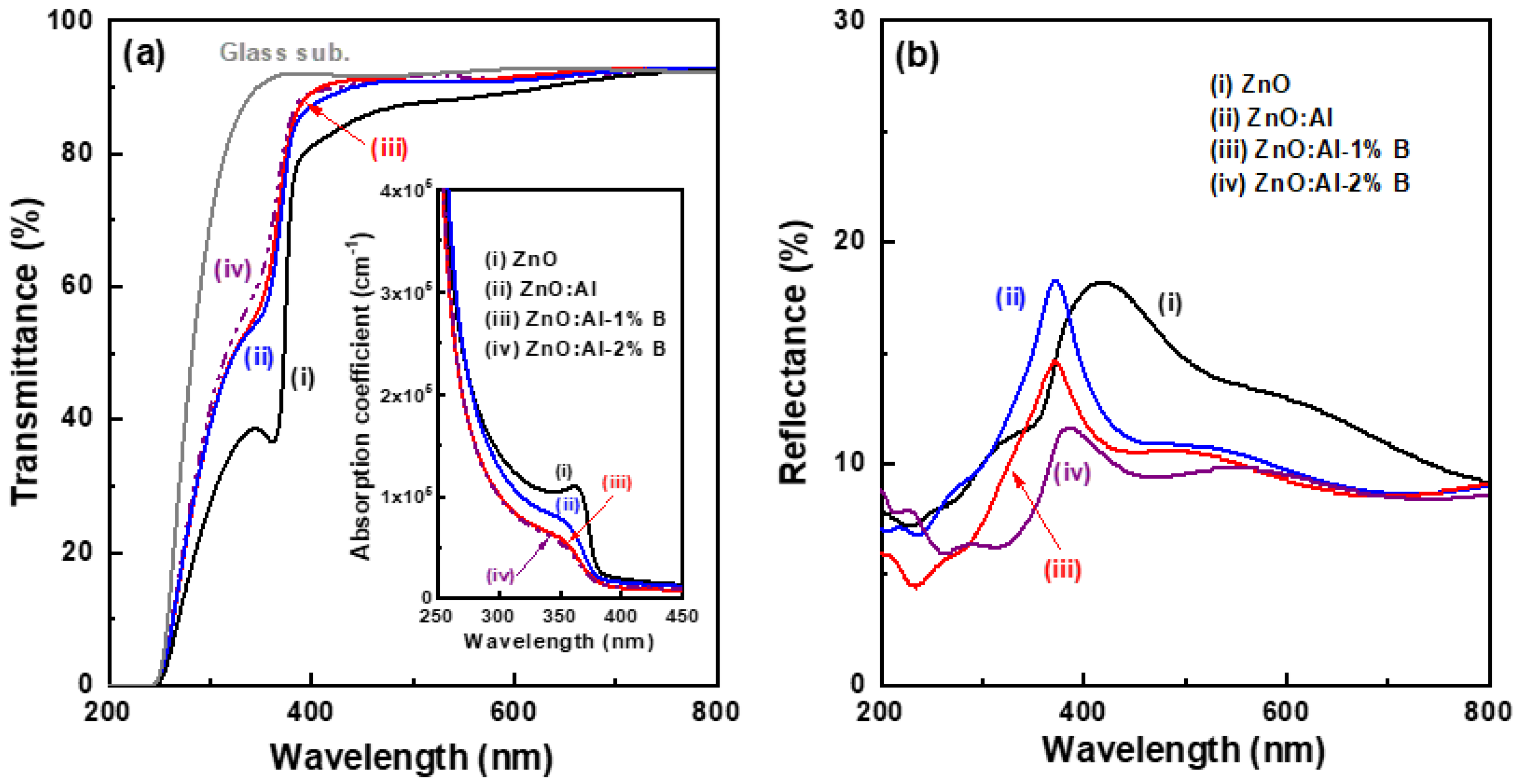
The transmittance and reflectance spectra of the glass/thin film samples were measured for investigation of the optical properties and are depicted in
Figure 5. These obtained ZnO-based thin films were highly transparent in the visible region, and their absorption edge (transmittance dramatically decreased) in the near UV region shifted toward the short wavelength region after the extrinsic doping. A strong absorption feature in the UV region of 350–400 nm was attributed to the intrinsic absorption that originated from the direct band-to-band transitions. Both Al-doped, and Al-B co-doped ZnO thin films exhibited high average transmittance (>91.3%) and low average reflectance (<10%) compared with the ZnO thin film in the visible region (400–800 nm), as shown in the fifth and sixth columns in
Table 2. The decreases in average reflectance with increasing dopant content can be ascribed to the extrinsically doped thin film samples having a flat free surface (see
Figure 3) and thus low scattering. In addition, the peak reflectivity near the absorption-edge wavelength can be ascribed to inter-band transitions in the oxide semiconductor [
30]. The ZnO:Al and ZnO:Al-B thin films exhibited higher average transmittance than that of the ZnO thin film because the extrinsically doped samples had a thinner thickness and flatter surface morphology than those of the undoped sample (see
Figure 2 and
Figure 3).
The first derivative of the optical transmittance (T) with the optical wavelength (λ) was computed for estimation of the absorption edge position of the oxide thin films. The curves of dT/dλ versus wavelength are presented in
Figure S2. The position of the maximum peak value corresponded to the optical band-edge absorption of the films [
5]. As shown in that figure, the peak position of the ZnO thin film was 375 nm, and the peak center positions of the singly doped and co-doped thin films varied from 372 nm to 368 nm. These results indicated that the absorption edge had shifted toward shorter wavelengths in the extrinsically doped samples.
The optical absorption coefficient (α) is an important parameter which can be utilized to estimate optical parameters, including the optical bandgap, Urbach energy, extinction coefficient and refractive index, for the modeling and design of optoelectronic devices. It is estimated from measured optical transmittance (
T) and reflectance (
R) data using the following formula [
31]:
where
t is the thickness of the obtained oxide thin film. Variation of the optical absorption coefficient (α) with wavelength is depicted in the inset of
Figure 5a. That plot shows that the magnitudes of absorption coefficients for ZnO, ZnO:Al and ZnO:Al-B had obvious discrepancies in the near UV region.
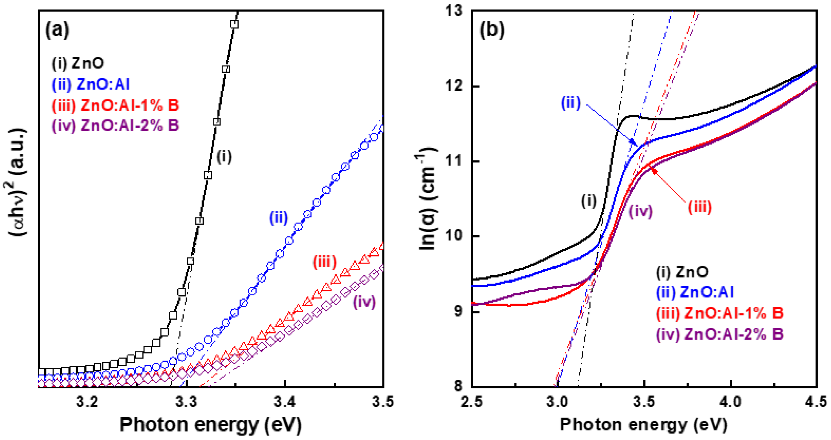
Optical transitions can occur as direct transitions between the valence band and conduction band in most wide-bandgap oxide semiconductors. Therefore, we evaluated the optical bandgap (
Eg) with allowed direct transitions for the four ZnO-based semiconductor thin films by using the following relation [
32]:
where
hν is the photon energy and the coefficient
A is an energy-independent factor relevant to the band tailing states. The plot of variation of (αhν)
2 with the photon energy (eV) (viz Tauc plot), calculated from the recorded transmittance and reflectance data, is shown in
Figure 6a. The optical bandgap (
Eg) of the thin films was determined by extrapolating the linear portion near the onset of the absorption edge of each absorption curve with the photon energy, hv (eV) on the X axis. The determined optical bandgap was slightly raised from 3.28 eV to 3.32 eV with increasing extrinsic dopant content (the second to last column in
Table 2). The estimated result for the as-prepared ZnO thin film was the same as that of the ZnO thin films grown via spray pyrolysis reported by Bedia et al. [
33] and ZnO thin films prepared through sol-gel spin coating reported by Gadallah et al. [
30]. The optical bandgap of the extrinsically doped thin film samples widened slightly, possibly in association with the increase in the electron concentration. The increased electron concentrations of the doped Al or co-doped Al-B in ZnO thin films first occupied the low energy level in the conduction band. When the ZnO-based thin film was irradiated with UV light, the photogenerated electrons could be excited from the valence band and move into the conduction band. If the low energy level in the conduction band was filled, the electrons would only jump to the high energy state, which corresponded to bandgap broadening [
4].
The dependence of the natural logarithm of the absorption coefficient (ln α) on the incident photon energy (
hν) near the band edge is known as the Urbach relation, which can be expressed as follows [
34,
35]:
where α
0 is a constant and
Eu is the Urbach energy of the semiconductor corresponding to the width of the band tail or the width of the localized state in the bandgap.
Figure 6b shows the plot of variation of ln (α) with photon energy, hν (eV) (namely, the Urbach plot). The Urbach energy was determined by calculating the inverse of the slope in the linear part of the absorption curve. We found that the Urbach energies of the obtained oxide thin films increased from 65.4 meV (ZnO) to 133.1 meV (ZnO:Al) and 168.0 meV (ZnO:Al-2% B), as shown in the
Table 2. These changes were attributed to degeneration of the film quality.
The refractive index (n) of the thin films is related to reflectance (
R), transmittance (
T) and extinction coefficient (
k) and is determined by the following formula [
30,
36].
where
k = αλ/4π is the extinction coefficient.
Figure 7 presents the extinction coefficient and refractive index of the four ZnO-based thin films dependent on the wavelength range of 300 nm to 800 nm. The extinction coefficient values for all thin film samples were below 0.07 for the visible light region, indicating that these as-prepared oxide thin films had a low dielectric loss (
Figure 7a). As shown in
Figure 7b, the refractive index decreased with increases in wavelength, which was associated with light scattering and absorption characteristics. The Sellmeier equation is generally used to determine the dispersion of light in functional oxide thin films. The high values of the refractive index for the ZnO and ZnO:Al samples were 2.49 at 418 nm and 2.54 at 372 nm, respectively. Such values were lower than that of a sol-gel derived ZnO thin film (n = 2.78 at almost 420 nm) reported by Yakuphanoglu et al. [
5]. It is also noted that the refractive index of the extrinsically doped samples was almost unaffected by changes in dopant content in the visible region.
This study demonstrated that the electrical and optical properties and the surface flatness of the transparent semiconductor ZnO thin films were significantly improved by incorporation of Al and B in the oxide thin films, but the crystallinity was degraded. The developed n-type ZnO transparent semiconductor thin films have a great potential to be used as active channel layer for thin-film transistors and sensing layers for UV photodetectors, and they could also be integrated as hole-blocking layers in organic solar cells.


