Article

Versatility of Nanocrystalline Silicon Films: from Thin-Film to Perovskite/c-Si Tandem Solar Cell Applications

Helmholtz-Zentrum Berlin für Materialien und Energie, Schwarzschildstr. 3, 12489 Berlin, Germany
*
Author to whom correspondence should be addressed.
Present address: Photovoltaic Materials and Devices Group, Delft University of Technology, 2628 CD Delft, The Netherlands.
Coatings 2020, 10(8), 759; https://doi.org/10.3390/coatings10080759
Submission received: 17 July 2020 / Revised: 27 July 2020 / Accepted: 28 July 2020 / Published: 3 August 2020
(This article belongs to the Special Issue Advances in Thin Films for Photovoltaic Applications)

Abstract

:
Doped hydrogenated nanocrystalline (nc-Si:H) and silicon oxide (nc-SiOx:H) materials grown by plasma-enhanced chemical vapor deposition have favourable optoelectronic properties originated from their two-phase structure. This unique combination of qualities, initially, led to the development of thin-film Si solar cells allowing the fabrication of multijunction devices by tailoring the material bandgap. Furthermore, nanocrystalline silicon films can offer a better carrier transport and field-effect passivation than amorphous Si layers could do, and this can improve the carrier selectivity in silicon heterojunction (SHJ) solar cells. The reduced parasitic absorption, due to the lower absorption coefficient of nc-SiOx:H films in the relevant spectral range, leads to potential gain in short circuit current. In this work, we report on development and applications of hydrogenated nanocrystalline silicon oxide (nc-SiOx:H) from material to device level. We address the potential benefits and the challenges for a successful integration in SHJ solar cells. Finally, we prove that nc-SiOx:H demonstrated clear advantages for maximizing the infrared response of c-Si bottom cells in combination with perovskite top cells.

1. Introduction

Hydrogenated nanocrystalline silicon (nc-Si:H) [1] thin films consists of a two-phase material of Si crystallites embedded in an hydrogenated amorphous silicon (a-Si:H) matrix. The material is commonly grown by plasma-enhanced chemical vapor deposition (PECVD) with highly hydrogen diluted silane flows and high-power/high-pressure plasma conditions. After Usui and Kikuchi [1] demonstrated the first semiconductor nc-Si:H film fabricated by silane glow discharge at low temperature in 1979, the material attracted great attention in the thin-film silicon community. This was because it extended the applicability of thin-film silicon layers deposited by PECVD at low temperatures (200 °C) for solar cells with the possibility to absorb light in the near-infrared range [2,3]. Due to effective defect passivation by hydrogen atoms, low enough defect densities are obtained making nc-Si:H a suitable NIR absorber layer with good carrier collection in typically 1–2 µm thick intrinsic layers. Layers were also successfully doped with boron or phosphorous yielding p- and n-type contact layers, respectively, as well as first p-i-n nc-Si:H solar cells [4]. In 1996, amorphous and nanocrystalline silicon was combined in a “micromorph” a-Si:H/nc-Si:H tandem solar cell [5]. As the light passes the entire layer stack several times due to light scattering, a significant optical loss originates from parasitic absorption in the doped layers. By adding oxygen-containing gas, usually CO2, to the PECVD process, nc-SiOx:H films with reduced absorption, low refractive index but still high (transversal) conductivity were obtained [6,7,8,9,10]. Tuning the refractive index by controlling the oxygen content opened the path for advanced applications in multijunction cells, e.g., as an intermediate reflecting layer between the two subcells [11,12,13,14], and building more complex multiple junction device [15].
In the early 1990s, Sanyo developed a new technology that combined crystalline silicon wafer-based absorbers with the materials and processing known from thin-film silicon technology to acting as passivated p- and n-contacts [16], thereby forming a-Si:H/c-Si silicon heterojunction (SHJ) solar cells. This device concept owns an exceptionally high open-circuit voltage up to 750 mV [17], achieved due to the excellent passivation of the c-Si surfaces by only a few nanometres thin intrinsic a-Si:H. The main limitation to the conversion efficiency in SHJ devices comes from photocurrent losses [18,19] due to parasitic absorption in the contact layers. Consequently, research efforts have been devoted to further increase the current extracted at the cell terminals by tailoring of the contact materials properties to reduce parasitic absorption of the incoming light in the front layer stack on top of the absorbing wafer.
Attempts of alloying a-Si:H layers with oxygen or carbon with the aim to widen the band gap and, therefore, minimize parasitic absorption led to enhanced transparency but reduced passivation and degraded electrical properties [20,21,22,23,24,25,26]. The alternative solution proposed is to apply thin Si-doped nanocrystalline layer with reduced absorption and suitable crystalline fraction embedded in the amorphous matrix to provide an efficient carrier transport. Differently to the previous dominant field of application in thin-film silicon solar cells, here, additional challenges arise: (i) obtain prompt nucleation of (ii) very thin nc-Si:H layers on (i)a-Si:H (iii) without deteriorating the c-Si surface passivation.
This work reviews the development and applications of hydrogenated nanocrystalline silicon oxide (nc-SiOx:H) focusing on its versatility and challenges in application in c-Si solar cells from two-sides contacted SHJ cells to monolithic tandem cells with perovskite top cells. We discuss the interplay between optical and electrical properties on solar cells parameters and strategies to overcome these issues.

2. Materials and Methods

Amorphous and nanocrystalline silicon films discussed here were deposited in an Applied Materials (AKT1600) PECVD cluster tool operating at 13.56 MHz with a parallel electrode configuration. To obtain nc-SiOx:H films, CO2 is added to the gas mixture. More details about deposition parameters and gas flows can be found elsewhere [27,28,29]. For optoelectrical characterization, single layers were deposited on glass substrates with a thickness of around 200 nm, unless specified in the text. We extracted thickness, refractive indexes and optical bandgap (E04) by fitting a Tau-Lorentz model to measured reflection and transmission spectra. The film conductivity was evaluated using coplanar mercury electrodes in dark at room temperature. Crystallinity fraction (FC) was derived from Raman scattering spectroscopy [30]. Layer stacks were deposited on glass substrates and consisted of a 6-nm thick (i)a-Si:H film coated with a 25-nm thick nanocrystalline layer to enable the investigation of the effect of substrate nature on FC.
Optical parameters of individual films were used as input data in OPAL 2 [31] or GenPro4 [32] software tools to simulate the photocurrent absorbed parasitically in each layer of single junction and tandem devices, respectively.
For SHJ solar cells fabrication, we used n-type FZ-Si wafers with chemically textured surfaces to obtain random pyramids with a process described in Ref. [33]. Intrinsic and doped silicon layers were grown on both sides of the wafer in front or rear junction configuration to obtain cell precursors. The cells were completed with sputtered transparent conducting oxide (TCO) layers on both sides [34] and screen-printed silver metal contacts.
Carrier lifetime of cell precursors was monitored using Sinton Instruments WCT-120 (Sinton Instruments, Boulder, CO, USA). The cells were characterized using an AAA+ dual-source sun simulator under standard test conditions through 4 cm2 shadow masks. From external quantum efficiency (EQE) on gridless cells, we quantified the current density by integrating the measured spectra over the spectral region of interest.

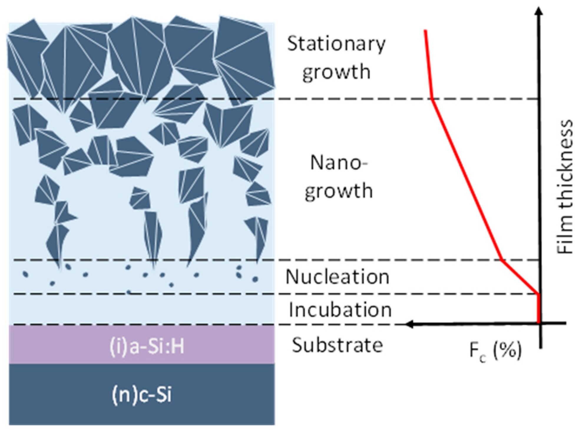
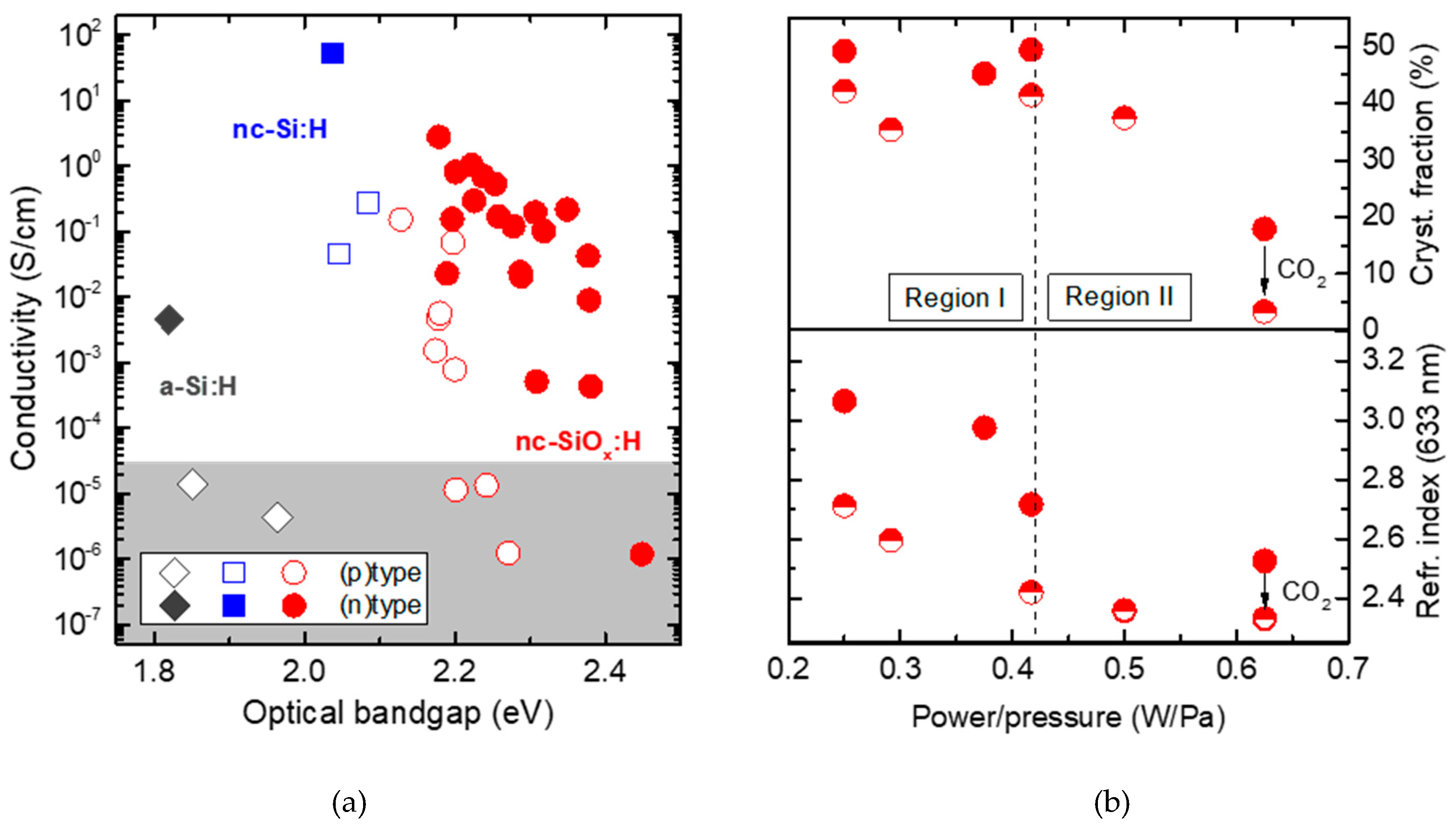
3. Nanocrystalline Silicon Material: Properties and Challenges

The PECVD deposition process is based on the dissociation of a gaseous silicon source, typically silane, SiH4 (pure or diluted in hydrogen gas, H2), in a plasma glow discharge. The precursor molecules undergo dissociation and subsequent reactions when they collide with high-energetic electrons in the plasma. Highly reactive growth precursors then diffuse to the substrate and lead to layer growth. An extensive analysis of the dissociation species is given in references [35,36,37].
Hydrogen atoms play an important role in the growth of high-quality a-Si:H and nc-Si:H films. More precisely, with increasing atomic hydrogen within the plasma, a higher crystalline fraction results, indicating that H plays a decisive role in the nc-Si:H evolution [38]. In the grown film, H atoms are preferentially located in the amorphous phase or at the crystal grain boundaries due to the low solubility of H into the crystalline phase [39], contributing to passivation of dangling bonds. The material can show a wide range of structure evolution from fully amorphous to highly crystalline depending on the deposition parameters [40,41,42]. In Figure 1, we show a simplified sketch of the evolution of a nc-Si:H film. It is based on a four stages approach as was proposed by Cabarrocas et al. [43] and later supported by in situ ellipsometry studies [44,45]. In particular, the authors identified the presence of a critical incubation zone which is believed to control the transition from the amorphous to the nanocrystalline regime affecting the evolution and, consequently, the properties of the entire nc-Si:H film. Afterwards, the nanocrystalline phase increases progressively until the growth becomes stationary. The cone-shape crystal growth of the nc-Si:H film makes the crystalline fraction variable along the film thickness [7,46]. This aspect also influences the electrical and optical properties of the layer until the zone of stationary growth is reached.
For SHJ solar cell application, the front-contact film stack is required to have a reduced thickness for low parasitic absorption, typically below 20 nm. Due to the directional evolution and the initial stages of growth, the material properties can widely vary within such thickness range. Moreover, the film has to grow on the (i)a-Si:H passivation layer that represents the substrate in a typical SHJ cell structures as depicted in Figure 1. It was demonstrated that (i)a-Si:H induces a thicker incubation phase among other substrates (i.e., c-Si, SiO2 or TCOs), which is most likely due to the permeability of the amorphous silicon layer to atomic H [43]. As a consequence, it delays the nucleation and reduces crystalline fraction in the bulk of (thin) films.
To find the optimum thickness for front doped layer, we report, in Figure 2, optical simulations of the front cell stack embedded between air and c-Si half space. The n, k spectra of the nc-Si:H and nc-SiOx:H layers are assumed to not depend on the layer thickness, therefore, here, the delayed nucleation is not taken into account. The photocurrent generated in the c-Si wafer drops linearly both for a-Si:H and nc-Si:H as depicted for both planar and textured substrates. On the contrary, we observe a completely different trend for the nc-SiOx:H on planar c-Si. As we discussed elsewhere [48], the more transparent oxide film and the front TCO layer form a stack with refractive indexes that progressively increase from air to the c-Si substrate leading to a gain in current for a thicker layer with a maximum for a ~40 nm thick nc-SiOx:H film with refractive index of ~2.7. More details on the effect of refractive indexes can be found in Ref. [49].
In conclusion, assuming textured c-Si, we would optically design the doped layer to be as thin as possible and, additionally, incorporate more oxygen to benefit from both reduced reflection losses and lower parasitic absorption. This might be in contrast to the complex structure of nanocrystalline material discussed above since the electronic properties also need to be taken into account. Therefore, to obtain a trade-off between the optical and electrical properties in nc-SiOx:H films is one the most critical aspects for their integration in solar cells. Figure 3a shows the abovementioned correlation between conductivity and optical bandgap for a variety of doped nc-Si:H and nc-SiOx:H layers in comparison to a-Si:H films. As discussed by Spear and Le Comber [50], n-type a-Si:H layers outperform the p-type ones. This trend is independent of the microstructure being amorphous or nanocrystalline [51]. Accordingly, Ding et al. [52] reported, for doped nc-SiOx:H layers, a similar oxygen content despite the strongly higher Fc of n-type films (above 60%) over p-type once (below 20%). This result suggests that the doping gas nature can influence the nanocrystalline evolution. Looking at the (p)nc-Si:H layers, we measure conductivities of ~10−1 S/cm. By incorporating more oxygen, the transparency improves with increasing E04 (and n) up to ~2.2 eV but with a degradation in conductivity with σ down to below 10−3 S/cm.
This effect can be partially explained by the reduced FC or due to lower doping efficiency of the film. For the n-doped films, we observe a similar trend but most of the layers still exhibit σ being above 10−3 S/cm even for E04 up to 2.4 eV.
Figure 3b show the effect of deposition power/pressure (P/p) and CO2 flows on crystalline fraction (FC) and refractive index (n). Similarly to what was studied in much more detail and discussed in Ref. [53], we observe two clear trends indicated as Region I and II. For the first region, we observe that the deposition conditions do not affect the FC, whereas the refractive index can be lowered down to 2.4, indicating more oxygen incorporation in the amorphous phase. The increase of P/p values strongly affect the crystalline fraction that rapidly decreases below 20% with a dominant amorphous fraction (region II). The arrows in Figure 3b show the effect of more CO2 in the gas mixture with reduced FC and n. This implicates that the careful choice of deposition parameters and gas mixture can lead to improved electrical properties and, at the same time, highly transparent layers that can be efficiently implemented at device level.

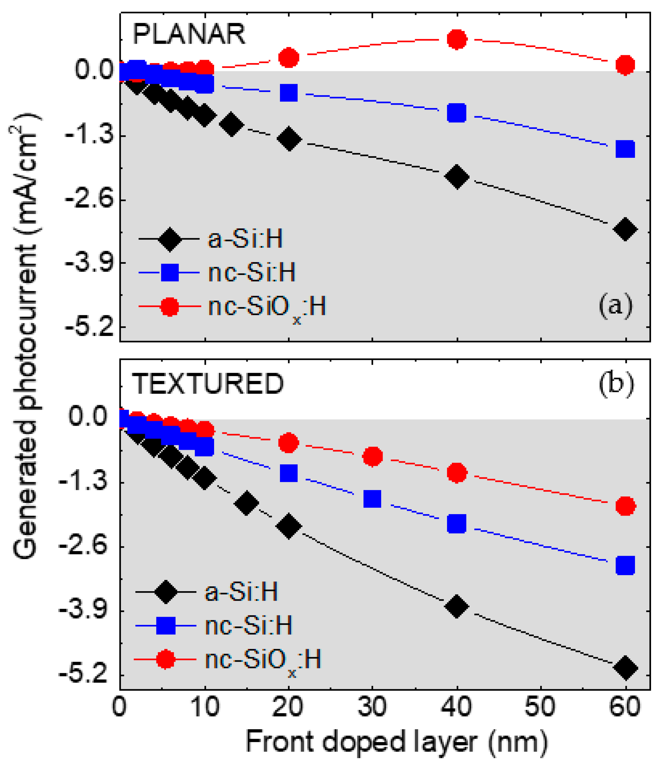
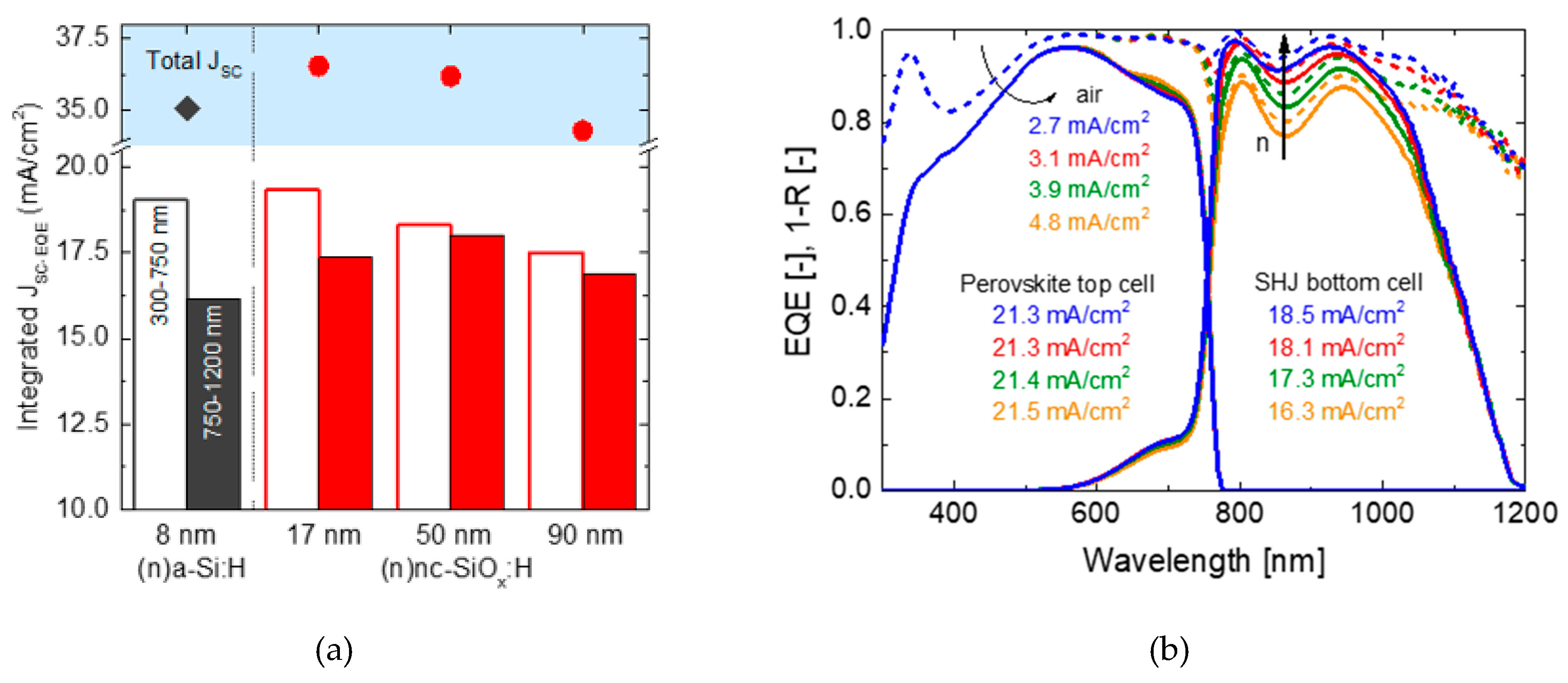
4. Strategies for Integration in SHJ Solar Cells

Besides the promising properties of doped nanocrystalline silicon layers, the integration in SHJ solar cells leads to some additional requirements and challenges. Looking at Figure 1, we can mention:
(a)
Fully amorphous incubation zone with lower doping efficiency and high resistivity.
(b)
High resistive bulk of the nc-Si:H or nc-SiOx:H layer.
(c)
A too low FC and, hence, low doping efficiency at the surface of the thin nanocrystalline film might lead to a poor tunnel-recombination (p)nc-Si:H/TCO contact.
The abovementioned aspects are in an interdependent relation since the initial stage of growth influences the nanocrystalline evolution in the bulk and, lastly, the final structural properties and the contact to the adjacent film. We discuss the first two aspects in the following section.

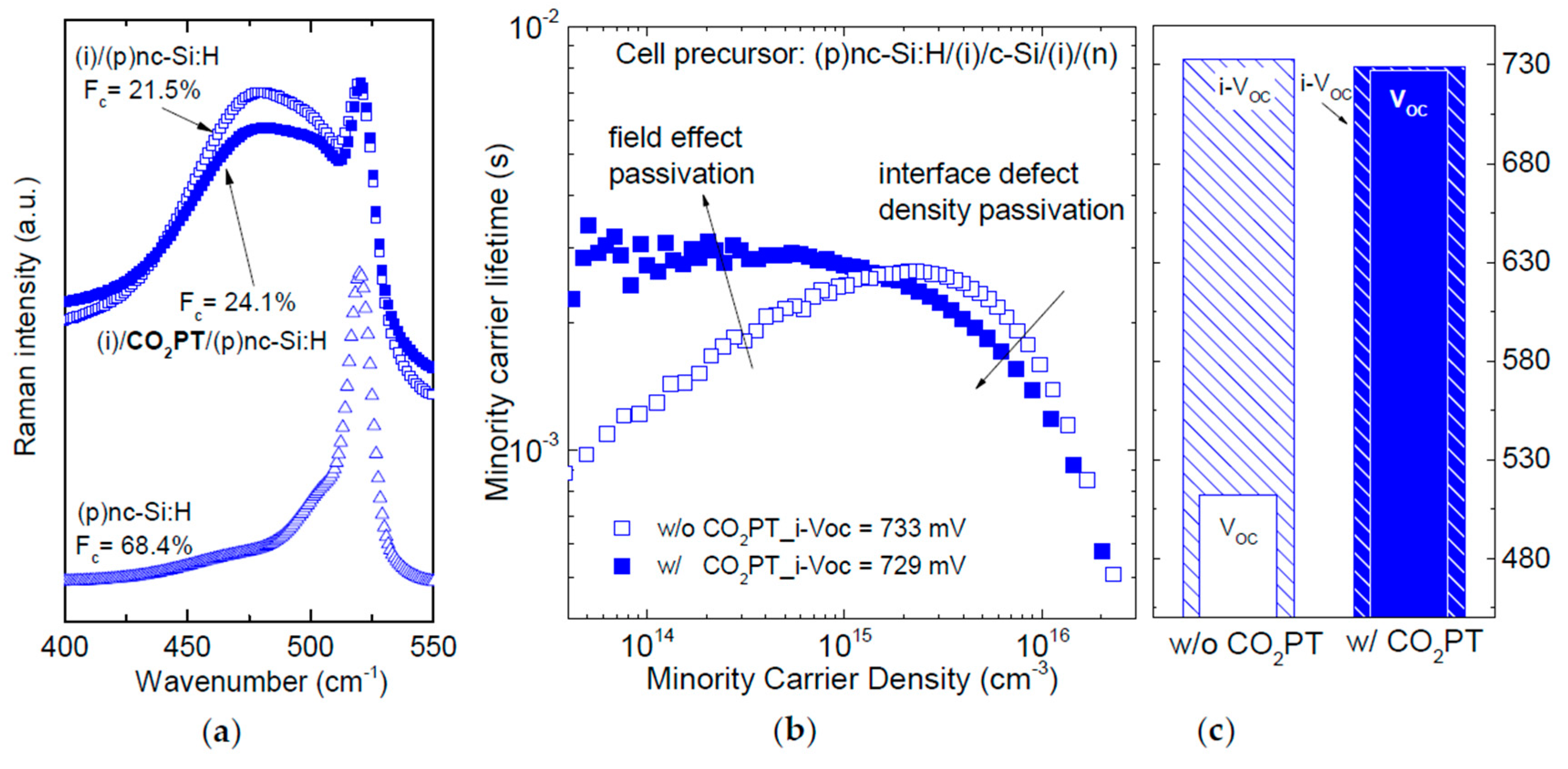
Nucleation Versus Passivation

In SHJ solar cells, doped layers are combined with a thin (i)a-Si:H layer that provides chemical passivation. When nanocrystalline films are grown on (i)a-Si:H substrates, we expect a delay in nucleation [43]. To give experimental evidence, Figure 4a shows Raman spectra of various samples. For 25-nm thick (p)nc-Si:H layers grown on either bare glass or on glass coated with a 6-nm thick (i)a-Si:H layer, we measure a drastic drop in FC from 68.4% to 21.5%, respectively.
To promote a faster crystallization of nanocrystalline silicon, as was implemented elsewhere [27,54,55], the (i)a-Si:H was treated with a soft and short CO2 plasma treatment (CO2PT) that can oxidize the surface [54,55,56], enhancing the nucleation of crystal growth. Alternatively, we also optimized the use of a nonoxidic and high crystalline/doped seed layer [28,57]. Other groups suggested alternative strategies, such as hydrogen plasma treatment, nonstandard Si source gases [45,58,59] and high excitation frequency [58,59,60,61] or lower deposition temperature [62].
Besides the crystallization, it is critical to investigate both the effect of the harsh deposition conditions, i.e., high plasma power and high density of hydrogen radicals, required for nanocrystalline growth and the influence of the CO2PT on the (i)a-Si:H passivation. For minority carrier lifetime measurements on cell precursors as shown in Figure 4b, we observe high passivation quality upon nc-Si:H deposition (i-VOC = 733 mV). The curve drops for low minority carrier density indicating a poor field-effect passivation due to the lower crystalline fraction as demonstrated in Figure 4a. In contrast, the optimized CO2PT results in a lifetime increase in the low injection region where the field-effect passivation is dominant, however, we observe a slight reduction of passivation quality with i-VOC of 728 mV. In Figure 4c, we compare the i-VOC of the cell precursors with the VOC measured on the completed device. The cell processed w/o CO2PT shows an J-V curve with low VOC (512 mV) and a strong S shape (not shown), on the contrary, the use of CO2PT results in a VOC very close to the implied one.
Both from the experimental observation shown in Figure 4 and from theoretical considerations [63,64,65], we can identify a minimum crystalline fraction of ~20%–30% for p-doped nanocrystalline silicon films, often indicated as percolation threshold, that ensure a structural connection within the nc-Si:H network. Usually, it is inferred by a rapid improvement in transport properties [63], and it can be an indication of the overcome of the incubation zone [65]. This can lead to an enhanced band bending and field-effect passivation with a higher space charge in the p-doped layer that can explain the results shown in Figure 4. Thus, we can infer that for the sample treated with CO2PT, the nc-Si:H overcomes the percolation threshold.

5. SHJ Solar Cells on Different Wafer Morphologies: the Path to Tandem Device

With c-Si cells approaching the practical conversion efficiency limit [66,67], alternative device architectures in tandem configuration are of great interest. Concurrently, solar cells based on high bandgap metal-halide perovskite absorbers quickly showed impressive efficiency. These factors result in a great interest of the scientific community in combining perovskite cells in tandem device with c-Si bottom cells with record efficiency of 29.15% [68,69].
Motivated by the better optical response of inverted perovskite architecture where the electron transport layer is placed at the front side [70], we focused on rear junction SHJ devices. In this configuration, the n-doped layer is placed at the front side of the SHJ cell.
Selected experimental Si solar cell parameters are displayed in Table 1 for devices optimized as single junctions. The short circuit currents confirm the expected gain discussed in Figure 2 by using nc-SiOx:H layer with appropriate thickness and refractive index. On textured c-Si, the n-layer with a total estimated thickness of only ~10 nm gives FF > 80% and VOC > 731 mV [28]. Besides cell efficiency of 22.5%, we demonstrated that nanocrystalline silicon oxide material also fulfil production requirements such as high throughput (60 s PECVD process time) and excellent cell homogeneity both in laboratory-scale [28] and in industry application [71]. The VOC on flat front side cells is relatively low as compared to the textured morphology partially due to the thicker c-Si wafers used to fabricate those devices (see Table 1). However, the (100) oriented polished c-Si surface is more difficult to passivate then the (111) oriented pyramid facets due to a tendency of epitaxial growth of the i layer [72].
For application of SHJ in tandem device, parasitic optical losses in the short wavelength range are not an issue since the perovskite top cell absorbs the light up to ~750 nm, and above this wavelength value, silicon thin films are very transparent. Therefore, we can modify the thickness of front layer stack with less optical constraints.
Figure 5a shows the current densities of various c-Si solar cells on flat front side fabricated with (n)nc-SiOx:H film with different thickness as shown in Ref. [74]. The integrated JSC values reported show that by increasing the (n)nc-SiOx:H thickness, the spectral response above 750 nm enhances due to lower IR reflection losses. We also observe a consistent enhancement by almost 2 mA/cm2 in the same wavelength range by comparing the (n)a-Si:H reference device to the cell with 50-nm thick (n)nc-SiOx:H.
Additionally, an increased NIR response using nc-SiOx:H film with appropriate thickness with a maximum at about 50 nm is visible.
This observation inspired the use of nc-SiOx:H interlayer to enhance the NIR response of the Si bottom cell in a perovskite/silicon tandem cell with a front-flat bottom cell [74], which is required for fabrication of perovskite top cells by solution processes. Alternatively, thermally evaporated perovskite layers allow the use of a textured c-Si bottom cell [75,76] for enhanced light trapping. However, wet processes still provide the best perovskite top cells.
Figure 5b reports simulated absorption profiles of tandem devices with the proposed approach using (n)nc-SiOx:H as both interlayer and active doped layer for the bottom cell. We demonstrated in Ref. [73] that the optical interlayer can manage the incoming light convening it in the bottom cell by reducing IR reflection losses. Both experimental results and optical simulations discussed in Ref. [73] show that the optimal interlayer should have a refractive index of 2.8 at 633 nm and a thickness of ~110 nm to maximize the result in 1.4 mA/cm2 IR current gain in the silicon bottom cell and stabilized device efficiency of 25.2% [73].

6. Conclusions

In this manuscript, we discuss the versatility of hydrogenated nanocrystalline silicon (nc-Si:H) materials for photovoltaic application. We give an overview of oxidic nc-Si:H film properties emphasizing on the unique combination of optical and electrical properties that made nanocrystalline material suitable for a wide range of solar cell applications.
We also widely present challenges and strategies for implementing nanocrystalline material in silicon heterojunction (SHJ) device. First, by means of optical simulation study, we identify the optimum layer thickness and transparency for application in SHJ cells. Subsequently, we discuss the delicate control of passivation and nanocrystalline growth comparing material properties, passivation results and solar cell parameters. We show that the use of CO2 plasma treatment prior nc-SiOx:H deposition can help to minimize the incubation zone and to faster develop a stable nanocrystalline growth.
Besides that, we show that also the contact to the front TCO might be very critical resulting in very poor fill factor devices. We solve this particular problem by inserting a nonoxidic contact layer that supports the tunnelling of holes thought this interface.
All these strategies resulted in a SHJ device with nc-SiOx:H with conversion efficiency of 22.5%, FF of 80.3%, VOC of 731 mV and JSC of 38.3 mA/cm2.
The final section is dedicated to the exploration of different c-Si device architectures. First, we show the optimization of SHJ cells on front flat c-Si substrate that shows the opportunity for current manipulating in the absorption in the infrared (IR) region of the spectrum. This observation motivates the use of nc-SiOx:H films in monolithic tandem devices with perovskite/c-Si cells to minimize the IR reflection losses. We show that the use of carefully designed interlayer gives a consistent gain in the current absorbed (+1.4 mA/cm2) in the bottom cells without affecting the top cell and the electrical parameters of the device.

Author Contributions

Conceptualization, L.M.; methodology, L.M. and A.B.M.-V.; investigation, L.M.; supervision, R.S., L.K., and B.S.; writing—original draft preparation, L.M. and B.S.; writing—review and editing, L.M. and B.S. All authors have read and agreed to the published version of the manuscript.

Funding

This research was funded by the German Federal Ministry of Economic Affairs and Energy within the project HERA, grant number 0325825 l, and the project PersiST, grant number 0324037C.

Acknowledgments

The authors thank Khalid Bhatti, Denise Debrassine, Alexandros Cruz Bournazou, Manuel Hartig, Tobias Hänel, Tobi Henschel, Kerstin Jacob, Sophie Kolb, Karolina Mack, Holger Rhein, Matteo Werth and Matthias Zelt for technical support.

Conflicts of Interest

The authors declare no conflict of interest.

References

  1. Usui, S.; Kikuchi, M. Properties of heavily doped GDSi with low resistivity. J. Non Cryst. Solids 1979, 34, 1–11. [Google Scholar] [CrossRef]
  2. Vetterl, O.; Finger, F.; Carius, R.; Hapke, P.; Houben, L.; Kluth, O.; Lambertz, A.; Mück, A.; Rech, B.; Wagner, H. Intrinsic microcrystalline silicon: A new material for photovoltaics. Sol. Energy Mater. Sol. Cells 2000, 62, 97–108. [Google Scholar] [CrossRef]
  3. Shah, A.V.; Meier, J.; Vallat-Sauvain, E.; Wyrsch, N.; Kroll, U.; Droz, C.; Graf, U. Material and solar cell research in microcrystalline silicon. Sol. Energy Mater. Sol. Cells 2003, 78, 469–491. [Google Scholar] [CrossRef] [Green Version]
  4. Fischer, D.; Dubail, S.; Servan, J.A.A.; Pellaton-Vaucher, N.; Platz, R.; Hof, C.; Kroll, U.; Meier, J.; Torres, P.; Keppner, H.; et al. The “micromorph” solar cell: Extending a-Si:H technology towards thin film crystalline silicon. In Proceedings of the Conference Record of the Twenty Fifth IEEE Photovoltaic Specialists Conference, Washington, DC, USA, 13–27 May 1996; pp. 4–7. [Google Scholar]
  5. Meier, J.; Torres, P.; Platz, R.; Dubail, S.; Kroll, U.; Selvan, J.; Koehler, J. On the way towards high efficiency thin film silicon solar cells by the “micromorph” concept. MRS Proc. 1996, 420, 683–684. [Google Scholar] [CrossRef]
  6. Das, D.; Mandal, S.; Barua, A. Intrinsic hydrogenated microcrystalline silicon oxide films prepared by RF glow discharge. J. Mater. Sci. Lett. 1998, 7, 2097–2100. [Google Scholar] [CrossRef]
  7. Cuony, P.; Marending, M.; Alexander, D.T.L.; Boccard, M.; Bugnon, G.; Despeisse, M.; Ballif, C. Mixed-phase p-type silicon oxide containing silicon nanocrystals and its role in thin-film silicon solar cells. Appl. Phys. Lett. 2010, 97, 213502. [Google Scholar] [CrossRef]
  8. Ding, K.; Aeberhard, U.; Smirnov, V.; Holländer, B.; Finger, F.; Rau, U. Wide gap microcrystalline silicon oxide emitter for a-SiOx: H/c-Si heterojunction solar cells. Jpn. J. Appl. Phys. 2013, 52, 122304. [Google Scholar] [CrossRef]
  9. Rattanapan, S.; Watahiki, T.; Miyajima, S.; Konagai, M. Improvement of rear surface passivation quality in p-type silicon heterojunction solar cells using boron-doped microcrystalline silicon oxide. Jpn. J. Appl. Phys. 2011, 50, 1–4. [Google Scholar] [CrossRef]
  10. Sritharathikhun, J.; Yamamoto, H.; Miyajima, S.; Yamada, A.; Konagai, M. Optimization of amorphous silicon oxide buffer layer for high-efficiency p-type hydrogenated microcrystalline silicon oxide/n-type crystalline silicon heterojunction solar cells. Jpn. J. Appl. Phys. 2008, 47, 8452–8455. [Google Scholar] [CrossRef]
  11. Dominé, D.; Buehlmann, P.; Bailat, J.; Billet, A.; Feltrin, A.; Ballif, C. Optical management in high-efficiency thin-film silicon micromorph solar cells with a silicon oxide based intermediate reflector. Phys. Status Solidi Rapid Res. Lett. 2008, 2, 163–165. [Google Scholar] [CrossRef]
  12. Cuony, P.; Alexander, D.T.L.; Perez-Wurfl, I.; Despeisse, M.; Bugnon, G.; Boccard, M.; Söderström, T.; Hessler-Wyser, A.; Hébert, C.; Ballif, C. Silicon filaments in silicon oxide for next-generation photovoltaics. Adv. Mater. 2012, 24, 1182–1186. [Google Scholar] [CrossRef] [PubMed]
  13. Kirner, S.; Calnan, S.; Gabriel, O.; Neubert, S.; Zelt, M.; Stannowski, B.; Rech, B.; Schlatmann, R. An improved silicon-oxide-based intermediate-reflector for micromorph solar cells. Phys. Status Solidi (C) 2012, 9, 2145–2148. [Google Scholar] [CrossRef]
  14. Yamamoto, K.; Nakajima, A.; Yoshimi, M.; Sawada, T.; Fukuda, S.; Suezaki, T.; Ichikawa, M.; Koi, Y.; Goto, M.; Meguro, T.; et al. A thin-film silicon solar cell and module. Prog. Photovolt. Res. Appl. 2005, 13, 489–494. [Google Scholar] [CrossRef]
  15. Kirner, S.; Neubert, S.; Schultz, C.; Gabriel, O.; Stannowski, B.; Rech, B.; Schlatmann, R. Quadruple-junction solar cells and modules based on amorphous and microcrystalline silicon with high stable efficiencies. Jpn. J. Appl. Phys. 2015, 54, 08KB03. [Google Scholar] [CrossRef]
  16. Tanaka, M.; Taguchi, M.; Matsuyama, T.; Sawada, T.; Tsuda, S.; Nakano, S.; Hanafusa, H.; Kumano, Y. Development of new a-si/c-si heterojunction solar cells: Acj-hit (artificially constructed junction- heterojunction with intrinsic thin-layer). Jpn. J. Appl. Phys. 1992, 31, 3518–3522. [Google Scholar] [CrossRef]
  17. Taguchi, M.; Yano, A.; Tohoda, S.; Matsuyama, K.; Nakamura, Y.; Nishiwaki, T.; Fujita, K.; Maruyama, E. 24.7% record efficiency HIT solar cell on thin silicon wafer. IEEE J. Photovolt. 2014, 4, 96–99. [Google Scholar] [CrossRef]
  18. Holman, Z.C.; Descoeudres, A.; Barraud, L.; Fernandez, F.Z.; Seif, J.P.; De Wolf, S.; Ballif, C. Current losses at the front of silicon heterojunction solar cells. IEEE J. Photovolt. 2012, 2, 7–15. [Google Scholar] [CrossRef] [Green Version]
  19. Holman, Z.C.; Filipič, M.; Descoeudres, A.; De Wolf, S.; Smole, F.; Topič, M.; Ballif, C. Infrared light management in high-efficiency silicon heterojunction and rear-passivated solar cells. J. Appl. Phys. 2013, 113, 013107. [Google Scholar] [CrossRef] [Green Version]
  20. Mazzarella, L.; Kirner, S.; Mews, M.; Conrad, E.; Korte, L.; Stannowski, B.; Rech, B.; Schlatmann, R. Comparison of TMB and B2H6 as precursors for emitter doping in high efficiency silicon hetero junction solar cells. Energy Procedia 2014, 60, 123–128. [Google Scholar] [CrossRef] [Green Version]
  21. Seif, J.; Descoeudres, A.; Filipič, M.; Smole, F.; Topič, M.; Charles Holman, Z.; De Wolf, S.; Ballif, C. Amorphous silicon oxide window layers for high-efficiency silicon heterojunction solar cells. J. Appl. Phys. 2014, 115, 024502. [Google Scholar] [CrossRef] [Green Version]
  22. Van Cleef, M.W.M.; Rubinelli, F.A.; Rizzoli, R.; Pinghini, R.; Schropp, R.E.I.; Van Der Weg, W.F. Amorphous silicon carbide/crystalline silicon heterojunction solar cells: A comprehensive study of the photocarrier collection. Jpn. J. Appl. Phys. 1998, 37, 3926–3932. [Google Scholar] [CrossRef]
  23. Pysch, D.; Bivour, M.; Hermle, M.; Glunz, S.W. Amorphous silicon carbide heterojunction solar cells on p-type substrates. Thin Solid Films 2011, 519, 2550–2554. [Google Scholar] [CrossRef]
  24. Mueller, T.; Duengen, W.; Ma, Y.; Job, R.; Scherff, M.; Fahrner, W.R. Investigation of the emitter band gap widening of heterojunction solar cells by use of hydrogenated amorphous carbon silicon alloys. J. Appl. Phys. 2007, 102, 074505. [Google Scholar] [CrossRef]
  25. Mueller, T.; Schwertheim, S.; Fahrner, W.R. Crystalline silicon surface passivation by high-frequency plasma-enhanced chemical-vapor-deposited nanocomposite silicon suboxides for solar cell applications. J. Appl. Phys. 2010, 107, 014504. [Google Scholar] [CrossRef]
  26. Mews, M.; Liebhaber, M.; Rech, B.; Korte, L. Valence band alignment and hole transport in amorphous/crystalline silicon heterojunction solar cells. Appl. Phys. Lett. 2015, 107, 1–4. [Google Scholar] [CrossRef] [Green Version]
  27. Mazzarella, L.; Kirner, S.; Gabriel, O.; Schmidt, S.S.; Korte, L.; Stannowski, B.; Rech, B.; Schlatmann, R. Nanocrystalline silicon emitter optimization for Si-HJ solar cells: Substrate selectivity and CO2 plasma treatment effect. Phys. Status Solidi Appl. Mater. Sci. 2017, 214, 1532958. [Google Scholar] [CrossRef]
  28. Mazzarella, L.; Morales-Vilches, A.B.; Korte, L.; Schlatmann, R.; Stannowski, B. Ultra-thin nanocrystalline n-type silicon oxide front contact layers for rear-emitter silicon heterojunction solar cells. Sol. Energy Mater. Sol. Cells 2018, 179, 386–391. [Google Scholar] [CrossRef]
  29. Morales-Vilches, A.B.; Mazzarella, L.; Hendrichs, M.; Korte, L.; Schlatmann, R.; Stannowski, B. Nanocrystalline vs. amorphous n-type silicon front surface field layers in silicon heterojunction solar cells: Role of thickness and oxygen content. In Proceedings of the 33rd European Photovoltaic Solar Energy Conference and Exhibition, Amsterdam, The Netherlands, 25–29 September 2017; pp. 715–719. [Google Scholar] [CrossRef]
  30. Klingsporn, M.; Kirner, S.; Villringer, C.; Abou-Ras, D.; Costina, I.; Lehmann, M.; Stannowski, B. Resolving the nanostructure of plasma-enhanced chemical vapor deposited nanocrystalline SiOx layers for application in solar cells. J. Appl. Phys. 2016, 119, 223104. [Google Scholar] [CrossRef] [Green Version]
  31. Mcintosh, K.R.; Baker-finch, S.C. OPAL 2.0: Rapid optical simulation of practical silicon solar cells. In Proceedings of the 29th IEEE Photovoltaic Specialists Conference, New Orleans, LA, USA, 19–24 May 2002. [Google Scholar]
  32. Santbergen, R.; Meguro, T.; Suezaki, T.; Koizumi, G.; Yamamoto, K.; Zeman, M. GenPro4 optical model for solar cell simulation and its application to multijunction solar cells. IEEE J. Photovolt. 2017, 7, 919–926. [Google Scholar] [CrossRef] [Green Version]
  33. Kegel, J.; Angermann, H.; Stürzebecher, U.; Conrad, E.; Mews, M.; Korte, L.; Stegemann, B. Over 20% conversion efficiency on silicon heterojunction solar cells by IPA-free substrate texturization. Appl. Surf. Sci. 2014, 301, 56–62. [Google Scholar] [CrossRef]
  34. Morales-Vilches, A.B.; Cruz, A.; Pingel, S.; Neubert, S.; Mazzarella, L.; Meza, D.; Korte, L.; Schlatmann, R.; Stannowski, B. ITO-free silicon heterojunction solar cells with ZnO: Al/SiO2 front electrodes reaching a conversion efficiency of 23%. IEEE J. Photovolt. 2019, 9, 34–39. [Google Scholar] [CrossRef] [Green Version]
  35. Perrin, J.; Leroy, O.; Bordage, M.C. Cross-sections, rate constants and transport coefficients in silane plasma chemistry. Contrib. Plasma Phys. 1996, 36, 3–49. [Google Scholar] [CrossRef]
  36. Knights, J.C.; Lujan, R.A.; Rosenblum, M.P.; Street, R.A.; Bieglesen, D.K.; Reimer, J.A. Effects of inert gas dilution of silane on plasma-deposited a-Si:H films. Appl. Phys. Lett. 1981, 38, 331–333. [Google Scholar] [CrossRef]
  37. Schmitt, J.P.M. Fundamental mechanisms in silane plasma decompositions and amorphous silicon deposition. J. Non Cryst. Solids 1983, 59–60, 649–657. [Google Scholar] [CrossRef]
  38. Matsuda, A. Formation kinetics and control of microcrystallite in µc-Si: H form glow discharge plasma. J. Non-Cryst. Solids 1983, 59–60, 767–775. [Google Scholar] [CrossRef]
  39. Itoh, T.; Yamamoto, K.; Ushikoshi, K.; Nonomura, S.; Nitta, S. Characterization and role of hydrogen in nc-Si: H. J. Non Cryst. Solids 2000, 266–269, 201–205. [Google Scholar] [CrossRef]
  40. Vallat-Sauvain, E.; Kroll, U.; Meier, J.; Shah, A.; Pohl, J. Evolution of the microstructure in microcrystalline silicon prepared by very high frequency glow-discharge using hydrogen dilution. J. Appl. Phys. 2000, 87, 3137–3142. [Google Scholar] [CrossRef] [Green Version]
  41. Houben, L.; Luysberg, M.; Hapke, P.; Carius, R.; Finger, F.; Wagner, H. Structural properties of microcrystalline silicon in the transition from highly crystalline to amorphous growth. Philos. Mag. A Phys. Condens. Matter Struct. Defects Mech. Prop. 1998, 77, 1447–1460. [Google Scholar] [CrossRef]
  42. Miyazaki, S.; Osaka, Y.; Hirose, M. Effects of growth rate on the microcrystalline characteristics of plasma-deposited μc-Si: H. Sol. Energy Mater. 1984, 11, 85–95. [Google Scholar] [CrossRef]
  43. Roca i Cabarrocas, P.; Layadi, N.; Heitz, T.; Drévillon, B.; Solomon, I. Substrate selectivity in the formation of microcrystalline silicon: Mechanisms and technological consequences. Appl. Phys. Lett. 1995, 66, 3609–3611. [Google Scholar] [CrossRef]
  44. Koh, J.; Ferlauto, A.S.; Rovira, P.I.; Wronski, C.R.; Collins, R.W. Evolutionary phase diagrams for plasma-enhanced chemical vapor deposition of silicon thin films from hydrogen-diluted silane. Appl. Phys. Lett. 1999, 75, 2286–2288. [Google Scholar] [CrossRef]
  45. Koh, J.; Fujiwara, H.; Koval, R.J.; Wronski, C.R.; Collins, R.W. Real time spectroscopic ellipsometry studies of the nucleation and growth of p-type microcrystalline silicon films on amorphous silicon using B2H6, B(CH3)3 and BF3 dopant source gases. J. Appl. Phys. 1999, 85, 4141–4153. [Google Scholar] [CrossRef]
  46. Richter, A.; Smirnov, V.; Lambertz, A.; Nomoto, K.; Welter, K.; Ding, K. Versatility of doped nanocrystalline silicon oxide for applications in silicon thin-film and heterojunction solar cells. Sol. Energy Mater. Sol. Cells 2017, 174, 196–201. [Google Scholar] [CrossRef]
  47. Mazzarella, L.; Kirner, S.; Stannowski, B.; Korte, L.; Rech, B.; Schlatmann, R. P-type microcrystalline silicon oxide emitter for silicon heterojunction solar cells allowing current densities above 40 mA/cm2. Appl. Phys. Lett. 2015, 106, 023902. [Google Scholar] [CrossRef]
  48. Mazzarella, L. Nanocrystalline Silicon and Silicon Oxide Contact Layers for Silicon Heterojunction Solar Cells. Ph.D. Thesis, Technischen Universität Berlin, Berlin, Germany, 2017. [Google Scholar]
  49. Mazzarella, L.; Morales-Vilches, A.B.; Hendrichs, M.; Kirner, S.; Korte, L.; Schlatmann, R.; Stannowski, B. Nanocrystalline n-type silicon oxide front contacts for silicon heterojunction solar cells: Photocurrent enhancement on planar and textured substrates. IEEE J. Photovolt. 2017, 8, 70–78. [Google Scholar] [CrossRef]
  50. Spear, W.E.; Le Comber, P.G. Electronic properties of substitutionally doped amorphous Si and Ge. Philos. Mag. 1976, 33, 935–949. [Google Scholar] [CrossRef]
  51. Lambertz, A.; Grundler, T.; Finger, F. Hydrogenated amorphous silicon oxide containing a microcrystalline silicon phase and usage as an intermediate reflector in thin-film silicon solar cells. J. Appl. Phys. 2011, 109, 113109. [Google Scholar] [CrossRef] [Green Version]
  52. Ding, K.; Aeberhard, U.; Lambertz, A.; Smirnov, V.; Holländer, B.; Finger, F.; Rau, U. Impact of doped microcrystalline silicon oxide layers on crystalline silicon surface passivation. Can. J. Phys. 2014, 92, 758–762. [Google Scholar] [CrossRef]
  53. Gabriel, O.; Kirner, S.; Klingsporn, M.; Friedrich, F.; Stannowski, B.; Schlatmann, R. On the plasma chemistry during plasma enhanced chemical vapor deposition of microcrystalline silicon oxides. Plasma Process. Polym. 2015, 12, 82–91. [Google Scholar] [CrossRef]
  54. Pellaton-Vaucher, N.; Rech, B.; Fischer, D.; Dubail, S.; Goetz, M.; Keppner, H.; Wyrsch, N.; Beneking, C.; Hadjadj, O.; Shklover, V.; et al. Controlled nucleation of thin microcrystalline layers for the recombination junction in a-Si stacked cells. Sol. Energy Mater. Sol. Cells 1997, 49, 27–33. [Google Scholar] [CrossRef] [Green Version]
  55. Pernet, P.; Goetz, M.; Keppner, H.; Shah, A. Growth of thin μc-Si: H on intrinsic a-Si: H for solar cells application. Mater. Res. Soc. Symp. Proc. 1997, 452, 889–894. [Google Scholar]
  56. Boccard, M.; Monnard, R.; Antognini, L.; Ballif, C. Silicon oxide treatment to promote crystallinity of p-type microcrystalline layers for silicon heterojunction solar cells. AIP Conf. Proc. 2018, 1999, 040003. [Google Scholar]
  57. Vetterl, O.; Hülsbeck, M.; Wolff, J.; Carius, R.; Finger, F. Preparation of microcrystalline silicon seed-layers with defined structural properties. Thin Solid Films 2003, 427, 46–50. [Google Scholar] [CrossRef]
  58. Seif, J.P.; Descoeudres, A.; Nogay, G.; Hanni, S.; De Nicolas, S.M.; Holm, N.; Geissbuhler, J.; Hessler-Wyser, A.; Duchamp, M.; Dunin-Borkowski, R.E.; et al. Strategies for doped nanocrystalline silicon integration in silicon heterojunction solar cells. IEEE J. Photovolt. 2016, 6, 1132–1140. [Google Scholar] [CrossRef]
  59. Djeridane, Y.; Abramov, A.; Roca i Cabarrocas, P. Silane versus silicon tetrafluoride in the growth of microcrystalline silicon films by standard radio frequency glow discharge. Thin Solid Films 2007, 515, 7451–7454. [Google Scholar] [CrossRef]
  60. Sriraman, S.; Agarwal, S.; Aydil, E.S.; Maroudas, D. Mechanism of hydrogen-induced crystallization of amorphous silicon. Nature 2002, 418, 62–65. [Google Scholar] [CrossRef] [PubMed]
  61. Hu, Y.Z.; Zhao, C.Y.; Basa, C.; Gao, W.X.; Irene, E.A. Effects of hydrogen surface pretreatment of silicon dioxide on the nucleation and surface roughness of polycrystalline silicon films prepared by rapid thermal chemical vapor deposition. Appl. Phys. Lett. 1996, 69, 485–487. [Google Scholar] [CrossRef]
  62. Fioretti, A.N.; Boccard, M.; Monnard, R.; Ballif, C. Low-temperature p-type microcrystalline silicon as carrier selective contact for silicon heterojunction solar cells. IEEE J. Photovolt. 2019, 9, 1158–1165. [Google Scholar] [CrossRef]
  63. Shimakawa, K. Percolation-controlled electronic properties in microcrystalline silicon: Effective medium approach. J. Non Cryst. Solids 2000, 266–269, 223–226. [Google Scholar] [CrossRef]
  64. Kim, D.Y.; Van Swaaij, R.A.C.M.M.; Zeman, M. Optical and electrical stimulation of µc-Si: H solar cells: Effect of substrate morphology and crystalline fraction. IEEE J. Photovolt. 2014, 4, 22–27. [Google Scholar] [CrossRef]
  65. Hamma, S.; Cabarrocas, P. Low-temperature growth of thick intrinsic and ultrathin phosphorous or boron-doped microcrystalline silicon films: Optimum crystalline fractions for solar cell applications. Sol. Energy Mater. Sol. Cells 2001, 69, 217–239. [Google Scholar] [CrossRef]
  66. Shockley, W.; Queisser, H.J. Detailed balance limit of efficiency of p-n junction solar cells. J. Appl. Phys. 1961, 32, 510–519. [Google Scholar] [CrossRef]
  67. Richter, A.; Hermle, M.; Glunz, S. Crystalline silicon solar cells reassessment of the limiting efficiency for crystalline silicon solar cells. IEEE J. Photovolt. 2013, 3, 1184–1191. [Google Scholar] [CrossRef]
  68. National Renewable Energy Laboratory (NREL). Best Research-Cell Efficiency Chart. Available online: https://www.nrel.gov/pv/cell-efficiency.html (accessed on 27 July 2020).
  69. Helmoholtz Zentrum Berlin (HZB). World Record: Efficiency of Perovskite Silicon Tandem Solar Cell Jumps to 29.15 per Cent. Available online: https://www.helmholtz-berlin.de/pubbin/news_seite?nid=21020,sprache=en;seitenid=1 (accessed on 27 July 2020).
  70. Jäger, K.; Korte, L.; Rech, B.; Albrecht, S. Numerical optical optimization of monolithic planar perovskite-silicon tandem solar cells with regular and inverted device architectures. Opt. Express 2017, 25, A473. [Google Scholar] [CrossRef]
  71. Morales-Vilches, A.B.; Decker, D.; Mazzarella, L.; Korte, L.; Schlatmann, R.; Sontag, D.; Stannoswki, B. Nanocrystalline n-type silicon front surface field layers: From research to industry applications in silicon heterojunction solar cells. In Proceedings of the 35th European Photovoltaic Solar Energy Conference and Exhibition, Brussels, Belgium, 28 September 2018; pp. 422–425. [Google Scholar]
  72. Olibet, S.; Vallat-Sauvain, E.; Fesquet, L.; Monachon, C.; Hessler-Wyser, A.; Damon-Lacoste, J.; De Wolf, S.; Ballif, C. Properties of interfaces in amorphous/crystalline silicon heterojunctions. Phys. Status Solidi Appl. Mater. Sci. 2010, 207, 651–656. [Google Scholar] [CrossRef]
  73. Mazzarella, L.; Lin, Y.; Kirner, S.; Morales-Vilches, A.B.; Korte, L.; Albrecht, S.; Crossland, E.; Stannowski, B.; Case, C.; Snaith, H.J.; et al. Infrared light management using a nanocrystalline silicon oxide interlayer in monolithic perovskite/silicon heterojunction tandem solar cells with efficiency above 25%. Adv. Energy Mater. 2019, 9, 1803241. [Google Scholar] [CrossRef]
  74. Mazzarella, L.; Werth, M.; Jäger, K.; Jošt, M.; Korte, L.; Albrecht, S.; Schlatmann, R.; Stannowski, B. Infrared photocurrent management in monolithic perovskite/silicon heterojunction tandem solar cells by using a nanocrystalline silicon oxide interlayer. Opt. Express 2018, 26, A487–A497. [Google Scholar] [CrossRef]
  75. Sahli, F.; Werner, J.; Kamino, B.A.; Bräuninger, M.; Monnard, R.; Paviet-salomon, B.; Barraud, L.; Ding, L.; Leon, J.J.D.; Sacchetto, D.; et al. Fully textured monolithic perovskite/silicon tandem solar cells with 25.2% power conversion efficiency. Nat. Mater. 2018, 17, 820–826. [Google Scholar] [CrossRef]
  76. Cojocaru, L.; Wienands, K.; Kim, T.W.; Uchida, S.; Bett, A.J.; Rafizadeh, S.; Goldschmidt, J.C.; Glunz, S.W. Detailed investigation of evaporated perovskite absorbers with high crystal quality on different substrates. ACS Appl. Mater. Interfaces 2018, 10, 26293–26302. [Google Scholar] [CrossRef] [PubMed]
Figure 1. Schematic cross-sectional sketch of the nanocrystalline silicon layer structure for a (i)a-Si:H-coated substrate. On the right, the FC evolution of the nanocrystalline phase is depicted as function of the film thickness for the different stages: incubation, nucleation, nanogrowth and stationary growth. Figure from [47].
Coatings 10 00759 g001
Figure 2. Simulated photocurrent absorbed in the c-Si wafer as a function of front doped layer thickness on (a) planar and (b) textured morphology. The nc-SiOx:H film used here has a refractive index of 2.7 at 633 nm. The values are reported as a difference relative to the structure with a 0 nm thick front layer. The grey areas indicate current losses. Figure adapted from [47].
Coatings 10 00759 g002
Figure 3. Simulated (a) electrical conductivity as function of optical band gap for p- and n- doped a-Si:H, nc-Si:H and nc-SiOx:H deposited at 300 and 500 H2/SiH4 ratio, respectively, and with various deposition parameters (i.e., power density, pressure and doping gas composition). Data adapted from [20,49]. The grey area indicates a critical regime where the bulk conductivity begins to contribute to the cell’s series resistance. (b) Top: Raman crystalline volume fraction and (b) Bottom: refractive index (at 633 nm) of doped (n)nc-SiOx:H from (a) as function of the power/pressure ratio and for variable CO2 flow (12–18 sccm). The other parameters are kept constant for all the films. The two deposition regimes are indicated as Region I and II. All the layers have a thickness in the range of 200–250 nm. Figure adapted from [47].
Coatings 10 00759 g003
Figure 4. (a) Raman spectra as function of wavenumber of (p)nc-Si:H film on variable substrate layers (laser 442 nm). The extracted value of crystalline fraction (FC) is reported next to each spectrum. (b) Minority carrier lifetime measured on precursors fabricated on textured wafers with and without a CO2 plasma treatment with the same 25-nm thick (p)nc-Si:H layer. (c) Implied-VOC extracted from (b) and VOC measured on the completed cells. Figure adapted from [47].
Coatings 10 00759 g004
Figure 5. (a) Experimental current densities from external quantum efficiency (EQE) spectra (JSC-EQE) of silicon heterojunction (SHJ) solar cells with a flat front side. The doped front layer is (n)a-Si:H or (n)nc-SiOx:H with variable thickness. Top part of the graph reports the total JSC-EQE, whereas the bottom shows the integrated value below/above 750 nm. Data adapted from [74]. (b) Simulated absorption in the absorbers (solid line) and 1-total reflection (dashed line) profiles of monolithic tandem devices on flat front side bottom cell with 50 nm (n)nc-SiOx:H layer and increased refractive index (arrow). The values represent the integrated currents absorbed in the perovskite and c-S absorbers and the losses due to reflection to the air. Figure adapted from [73].
Coatings 10 00759 g005
Table 1. J-V parameters of best solar cells fabricated on both-sides-textured and 1-side-textured c-Si wafers with (n) doped nc-Si:H and nc-SiOx:H placed on the front side. Data from [28,73].
Substrate Front/RearMaterialt (nm)JSC (mA/cm2)VOC (mV)FF (%)H (%)
TEXT/TEXT(n)nc-Si:H1237.872979.721.9
(n)nc-SiOx:H1038.373180.322.5
FLAT/TEXT(n)nc-SiOx:H1735.771979.720.5

