Article

Photocatalytic Bi2O3/TiO2:N Thin Films with Enhanced Surface Area and Visible Light Activity

Centre of Physics, University of Minho, 4835-386 Guimarães, Portugal
*
Author to whom correspondence should be addressed.
Coatings 2020, 10(5), 445; https://doi.org/10.3390/coatings10050445
Submission received: 3 April 2020 / Revised: 24 April 2020 / Accepted: 26 April 2020 / Published: 1 May 2020
(This article belongs to the Special Issue Photocatalytic Thin Films)

Abstract

:
Bi2O3 nanocone films functionalized with an overlayer of TiO2 were deposited by d.c. reactive magnetron sputtering. The aforementioned nanocone structures were formed via a vapour-liquid-solid (VLS) growth, starting from a catalytic bismuth seed layer. The resultant nanocones exhibit an improved surface area, measured by atomic force microscopy, when compared to non-VLS deposition of the same metal oxide. X-ray diffraction texture analysis enabled the determination of the crystallographic β-phase of Bi2O3. A very thin TiO2 overlayer (6 nm thick), undoped and doped with nitrogen, was deposited onto the nanocones template, in order to functionalize these structures with a photocatalytic, self-cleaning, cap material. N-doped TiO2 overlayers increased the selective absorption of visible light due to nitrogen doping in the anatase cell, thus, resulting in a concomitant increase in the overall photocatalytic efficiency.

1. Introduction

Photocatalytic materials are commonly used in the industry for water and air de-pollution systems [1,2]. In the majority of cases, these photocatalytic processes involve the illumination of a semiconductor material with ultraviolet (UV) light [3,4]. From this activation, hydroxyl radicals with a high oxidation potential are created from the inherent oxidation-reduction mechanisms on the photocatalyst surface [5], which lead to the mineralisation of adsorbed pollutants. Titanium dioxide is a preferable choice for a photocatalyst, in several forms, such as in films [6], nanoparticles [7], nanotubes [8,9], functionalized polymers and membranes [10,11,12], amongst others. This material is known for its low level of toxicity and relatively high chemical stability, which envisages the aforementioned applications. Conversely, its rather large bandgap energy of 3.2 eV, for the anatase prevailing phase, limits its effectiveness while using the full solar radiation spectrum [13]. Hence, an opportunity has arisen in recent years to enhance the absorption of visible light in TiO2 [1,14,15]. Anionic doping of TiO2 has proven to have a positive effect on the absorption of visible light, in particular, substitutional of oxygen atoms in the anatase cell for nitrogen atoms [6,16,17]. This anionic doping is efficient as long as the O 2p and N 2p orbitals overlap in the valence band, in order to inhibit the formation of defect levels inside the gap, which are active recombination centres. Another possibility is to functionalise, or couple, TiO2 with another metal-oxide semiconductor with smaller band-gap, in order to enhance visible light-induced photocatalysis from this coupling effect [18,19]. Some publications have recounted the photocatalytic efficiency of bismuth oxide (Bi2O3) films [20]. Bi2O3 has several polymorphs (α, β, δ, γ e ε), being the α an β phase those with greater photocatalytic efficiency, with a direct energy gap in the range of 2.7–3.4 eV [21]. However, certain authors have reported mixed indirect/direct band-gaps in the range of 1.6–2.7 eV for polycrystalline Bi2O3 films comprising the latter polymorphs [22,23,24,25,26]. A high specific surface area is developed in this material when produced in the form of nanocones [24], which promotes the photocatalytic ability when generating more adsorption sites for pollutants.
In this work, Bi2O3 films with nanocone morphology and high projected surface area were produced as layer templates for the deposition of undoped and N-doped TiO2 photocatalytic overlayer thin films. Bi2O3 nanocones structures were developed through a vapour-liquid-solid mechanism (VLS) [27]. The rationale evolved from the hypothesis that by functionalisation of both metal oxides, TiO2 and Bi2O3, a heterojunction is created with a broader absorption spectrum [28,29]. Since the semiconductor conduction and valence bands of Bi2O3 are more anodic than those of TiO2, the excited electrons in the TiO2 conduction band can be transferred to the Bi2O3 conduction band and participate actively in the photocatalysis mechanisms [29]. In particular, by actively reducing oxygen (electron scavengers), which subsequently leads to the superoxide (O2) radical species formation, which, in turn, disproportionates to H2O, hydroperoxide anion (HO2) and hydroxyl (OH) radicals with a very high (2.8 V) oxidation potential.

2. Experimental Details

All layers were deposited on silicon and glass substrates by dual unbalanced reactive magnetron sputtering, by means of a high-vacuum chamber with a base pressure of ~10−4 Pa (Figure 1). Two metallic targets were used as cathodes, Bi and Ti of high purity (99.95%) and (99.8%), respectively, having dimensions of 101 mm (diameter) × 6.1 mm (thickness). In order to prevent contamination of the layers, the substrates were washed in ultrasounds with an isopropyl solution for 20 min, prior to loading into the 6-fold carrousel substrate holder (Figure 1). Furthermore, before layer deposition, a plasma etching at a pressure of 1.8 Pa was performed during 3−5 min for further cleaning of the substrates and targets. In this configuration, the working gas (argon) is fed directly on the target surface, whereas the reactive gases (oxygen and nitrogen) are fed closer to the substrates. The latter feature presents a major modification in regard to a previous report [28], since the quality of the films is substantially enhanced. During all depositions, the substrate temperature was fixed at 175 °C, and the target-to-substrate distance was set to 9 cm. The remaining process parameters for the deposition of all layers are listed in Table 1. Initially, the process parameters for the initial Bi seed layer were kept constant before introducing the reactant oxygen gas in the chamber for the subsequent Bi2O3 layer formation by VLS. Finally, a 6 nm thick TiO2 overlayer was deposited, with and without N-doping, on top of the Bi2O3 nanocones, conferring to the process parameters listed in Table 1.
The crystalline structure and texture of the Bi2O3 layers was characterized using an X-ray diffractometer (Bruker AXS D8 Discover, Karlsruhe, Germany) with a multiple circle goniometer and Eulerian cradle, illuminated by CuKα radiation. The surface topography was studied using a scanning electron microscope (SEM, NanoSEM-FEI Nova 200, FEI, Hillsboro OR, USA). X-ray photoelectron spectroscopy measurements were carried out using monochromatic Al-Kα radiation (1486.6 eV) from a Kratos Axis-Supra instrument (Kratos, Manchester, United Kingdom). Transmittance and reflectance spectra were measured with a Shimadzu UV-2501PC spectrophotometer with an integrating sphere (Shimadzu, Kyoto, Japan). The surface roughness and projected surface area of the layers were measured by atomic force microscopy (AFM, Digital Instruments Nanoscope III, Bruker AFM, Santa Barbara, CA, USA). The evaluation of the photocatalytic efficiency of the photocatalytic layers was studied by monitoring the mineralisation of a dye, methylene blue (MB, 10−5 M), under UV-A and visible light irradiation. For this, Bi/Bi2O3/TiO2 and Bi/Bi2O3/TiO2:N layers were immersed in a quartz cuvette with the dye, under magnetic stirring with the film side facing the lamp source. The MB dye most relevant absorption peak at 665 nm was monitored as a function of time using a ScanSci high resolution spectrometer (ScanSci, Porto, Portugal). UV-A radiation was centred at 365 nm with a 700 mA high-power LED source (Thorlabs, Newton, NJ, USA, while for visible light excitation an Oriel Xe lamp (Newport-Oriel, Irvine, CA, USA) was used, with an average irradiance of 2 mW/cm2.

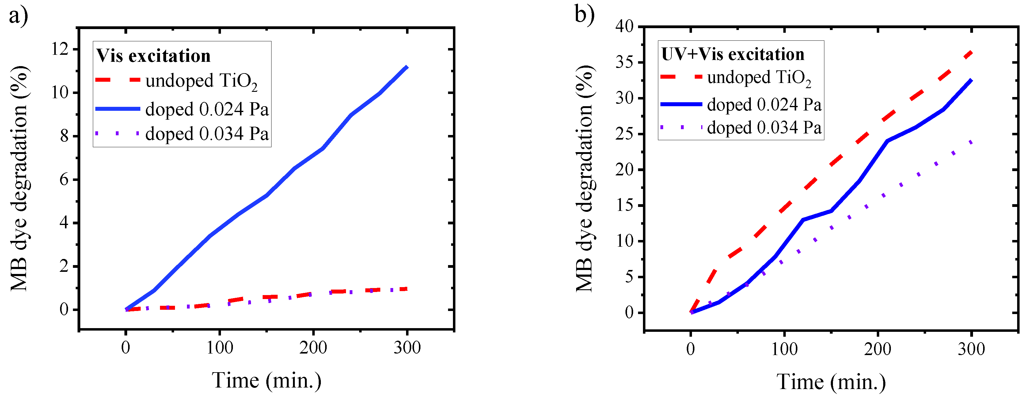
3. Results and Discussion

Figure 2 shows the morphology of the surface (Figure 2a,b) and cross-section (Figure 2c) of Bi2O3 layers grown by VLS from an initial Bi seed layer that was sputtered in an argon atmosphere with a deposition rate of 200 nm/min for 2 min. Subsequently, reactive oxygen gas was introduced with a partial pressure of 0.14 Pa for the Bi2O3 layer, while maintaining all other deposition process parameters constant (Table 1). From Figure 2a, and at higher magnification in Figure 2b, a dendritic nanocone growth can be observed. Furthermore, on the surface of the Bi2O3, Bi-metal droplets are discerned, which are active centres that promote the nanocone formation. In the cross-section micrograph of Figure 2c, the formation of both Bi and Bi2O3 layers can be readily observed. The dendritic growth can be abnormally high in some zones of the sample surface, reaching a maximum of 2.5 μm height from the substrate. The metallic Bi seed layer shows relatively large columns, typical of Zone II in Thornton’s model, whereas the Bi2O3 layer has narrower columns, tightly packed fibrous grains, typical of zone T in the same model [30].
Atomic force microscopy analysis enabled the determination of the roughness and projected surface area parameters of the Bi2O3 layers. These quantities were calculated using the statistical algorithms included in the Gwyddion software package [31], in particular, the mean roughness, Ra, and root mean square roughness, Rq. An AFM micrograph of the surface of Bi2O3 layers is presented in Figure 3, with Ra = 133 ± 2 nm and Rq = 155 ± 2 nm, and a calculated projected surface area of 48 μm2. This relatively large induced roughness from the dendritic growth of the Bi2O3 layers is important for enhancing the adsorption of pollutants and their subsequent photocatalytic mineralisation.
Figure 4 shows the X-ray diffraction (XRD) pattern for a Bi2O3 layer, with respective Rietveld fit, where the β-Bi2O3 (tetragonal) phase can be indexed to the P-421c space group (ICDD crystallographic card number 01-077-5341), with lattice parameters a = 7.744 Å and c = 5.659 Å; the most relevant reflections from diffracting planes are labelled. No other relevant Bi2O3 phases are detected. The resulting film is polycrystalline with predominant diffraction from the (201) planes at 27.92°. An average crystallite size of 27 ± 3 nm was derived from the Rietveld fit over whole diffraction pattern.
Some authors have reported on the difficulty in indexing XRD patterns to Bi2O3 due to the overlap or contiguous diffraction peaks from other polymorph phases, in particular at lower diffraction angles from α- (monoclinic, P21/c), γ- (cubic, I23) and/or δ- (cubic, Fm-3m) Bi2O3 phases [32], especially if these phases are slightly strained. Bearing this in mind, texture analysis was performed, and the resulting pole figures and 3-D contour plots are displayed in Figure 5. The texture was surveyed for the reflections from (201) at 27.92°, (002) at 31.57° and (220) at 32.70° diffracting planes, being acquired in an azimuth range (Φ) of 0°–360° and a tilt range (Ψ) of 0°–90°, with 5° steps and 1s integration time. The diffraction rings in Figure 5a,c,e, and respective 3-D contours in Figure 5b,d,f were obtained for Ψ angles of 55.59°, 54,31° and 55.59°, representing angles between (201)˄(002), (220)˄(201) and (002)˄(201), respectively. These pole figures are consistent with a tetragonal crystal system.
In Figure 6, the XPS spectra and respective fits are exposed to the main photoelectron lines of the Bi/Bi2O3/TiO2 heterostructured coating. From Figure 6a, the Bi 4f core level was fitted with two peak doublets with a spin-orbit energy separation of 4f5/2 − 4f7/2 = 5.3 eV and a peak area ratio A4f5/2/A4f7/2 = 0.75. Two contributions were fitted, with Bi 4f7/2 binding energies of 156.4 eV and 158.7 eV, which correspond to the metallic bismuth and oxidation state of Bi3+ in Bi2O3, respectively [33]. Bi-metal contribution is expected from the metal droplets on the surface, as seen in Figure 2a,b. The TiO2 overlayer is very thin and amorphous (6 nm) and, hence, does not cover all of the underlying Bi2O3 layer. Regarding the O 1s core line in Figure 6b, this was fitted with three components: the main component at 530.2 eV (comp.1) is ascribed with Bi–O and Ti–O bonds; the second component (comp.2) centred at 531.3 eV is associated with defective oxygen (vacancies) in both Bi2O3 and TiO2 layers, although it should be more related with the latter; the third component (comp.3) centred at 532.2 eV is associated with adsorbed oxygen contaminants (OH, CO) [34]. The relative areas of these three O 1s contributions are 67%, 15% and 18%, respectively. Lastly, in Figure 6c is presented the XPS fit for the Ti 2p core level, where the spin-orbital splitting of 5.7 eV between Ti 2p3/2 (458.7 eV) and Ti 2p1/2 (464.4 eV) is apparent, with a peak area ratio A2p1/2/A2p3/2 = 0.5, which is in agreement with the literature for TiO2 [34].
In order to study the photocatalytic activity, the kinetics of methylene blue dye degradation were followed in the presence of Bi/Bi2O3/TiO2 and Bi/Bi2O3/TiO2:N heterostructured films, under visible irradiation (>400 nm) and UV-A plus visible irradiation (>365 nm). These experiments are shown in Figure 7. When using visible light excitation (Figure 7a), the TiO2 overlayer deposited with a reactive N2 partial pressure of 0.024 Pa has a much higher photocatalytic efficacy compared to undoped TiO2 overlayer and N-doped TiO2 overlayer deposited with higher partial pressure (0.034 Pa). This is indicative that N-doping in TiO2 enhances the absorption of visible light. This feature was observed in three sets of samples with the same undoped and doped conditions. The first-order rate constant (k) for the degradation of MB can be calculated from the following relation: C0 and C are the initial concentration and concentration at a specific time (t) of the MB dye, which follows first-order kinetics with time: (C0C) = C0·ekt. Following this, k is 4 × 10⁻⁵ min−1, 4 × 10⁻⁴ min−1 and 4 × 10⁻⁵ min−1 for undoped TiO2, doped with 0.024 Pa and 0.034 Pa of N2 during deposition, respectively. When illuminating the samples with both UV and visible light (Figure 7b) the undoped TiO2 overlayer performs as well as the N-doped (0.024 Pa), both with k = 2 × 10⁻³ min−1. As in the case of excitation solely with visible illumination, when combining excitation of UV and visible, the N-doped TiO2 overlayer grown with a higher N2 partial pressure (0.034 Pa) performs worse (k = 9 × 10⁻⁴ min−1). The reason for this is attributed to the amount of N-doping that the anatase structure can accommodate without being excessive and resulting in defect states that will promote electron/hole recombination and, subsequently, hinder photocatalysis [6].
From the optical transmittance (T) and reflectance (R) of Bi2O3 and TiO2:N films on glass substrates, with a thickness (d) of 480 nm and 6 nm, respectively, the absorption coefficient, α = (1/dln[(100−R)/T] was calculated [35]. Subsequently, and employing a relation between the absorption coefficient and photon energy, α = (A/)·(Eg)m, where A is a parameter independent of the photon energy, hν (h is Planck’s constant; ν is photon frequency), and m a value representing the optical transition mode (m = 0.5 for the direct band-gap; m = 2 for the indirect band-gap), Eg was extrapolated from the interception with the photon energy axis, as represented in the Tauc plots of Figure 8 [35]. From this linear regression, confidence and prediction bands (>95%) are plotted and highlighted by the pink lines. The band-gap, Eg, for TiO2:N is much higher (3.69 ± 0.01 eV) when compared to the known bulk value for TiO2 (anatase polymorph) with indirect band-gap of 3.20 eV [36]. However, the TiO2:N overlayer is only 6 nm thick and amorphous, hence the disparity. It would be expected for thicker and crystalline TiO2 films that the band-gap would be more approximate to the bulk value. Contrariwise, the Eg value for the Bi2O3 layer (3.12 ± 0.01 eV) is within the extended range that has been reported in the literature for β-Bi2O3 films, between 2.7 and 3.4 eV [37,38].

4. Conclusions

Bi2O3 template layers with enhanced surface area in the form of nanocone structures were deposited by reactive magnetron sputtering from an initial Bi seed layer following a vapour-liquid-solid mechanism. The resulting microstructure is polycrystalline, being the tetragonal β-phase dominant, as confirmed by XRD combined with texture analysis. XPS provided evidence for metallic bismuth and the oxidation state of Bi3+ in the Bi2O3 layer, being the metal contribution ascribed to the seed crystals that originate the nanocones through the VLS growth mechanism. AFM measurements enabled the determination of the surface roughness (Rq = 155 ± 2 nm) and projected surface area (48 μm2, for 5 μm × 5 μm scans), which is considerably high for a thin film, owing to the dendritic nanocone structure. From measurements of the degradation kinetics of MB dye degradation under UV-A and visible illumination, it was concluded that the Bi/Bi2O3/TiO2:N layers increased the absorption of visible light, by being more efficient to degrade the test pollutant, when compared to Bi/Bi2O3/TiO2 layers. Hence, these heterostructured layers are innovative and promising photocatalytic materials for the de-pollution of toxic organic volatile compounds present in air, as well of strong chromophores diluted in residual wastewater. In future work, a different anionic doping or even cationic doping of TiO2 will be pursued to further enhance the absorption of visible light. Currently, these Bi/Bi2O3/TiO2:N heterostructured layers are being tentatively applied in air purification units, within the mainframe of a collaboration with a Portuguese industry, Vieira & Lopes Lda.

Author Contributions

Conceptualization, C.J.T.; methodology, C.J.T.; software, C.J.T.; validation, C.J.T. and L.P.D.; formal analysis, C.J.T.; investigation, L.P.D, J.M.R., F.C.C; resources, C.J.T.; data curation, L.P.D, C.J.T.; writing—original draft preparation, C.J.T.; writing—review and editing, L.P.D, C.J.T.; visualization, L.P.D., F.C.C., J.M.R., C.J.T.; supervision, C.J.T.; project administration, C.J.T.; funding acquisition, C.J.T. All authors have read and agreed to the published version of the manuscript.

Funding

The authors acknowledge the financial support of the project “NANOPURIFY—Development of photocatalytic panels for air treatment units, Vieira & Lopes Lda.”, with the reference 024121, co-funded by the European Regional Development Fund (ERDF), through the Operational Programme for Competitiveness and Internationalisation (COMPETE 2020), under the PORTUGAL 2020 Partnership Agreement. Filipe C. Correia acknowledges the financial support from the Fundação para a Ciência e Tecnologia (FCT) for the Ph.D grant SFRH/BD/111720/2015.

Conflicts of Interest

The authors declare no conflict of interest. Moreover, the funders had no role in the design of the study; in the collection, analyses, or interpretation of data; in the writing of the manuscript, or in the decision to publish the results.

References

  1. Zaleska-Medynska, A. Doped-TiO2: A Review. Recent Patents Eng. 2008, 2, 157–164. [Google Scholar] [CrossRef]
  2. Nakata, K.; Fujishima, A. TiO2 photocatalysis: Design and applications. J. Photochem. Photobiol. C Photochem. Rev. 2012, 13, 169–189. [Google Scholar] [CrossRef]
  3. Fujishima, A.; Rao, T.N.; Tryk, D.A. Titanium dioxide photocatalysis. J. Photochem. Photobiol. C Photochem. Rev. 2000, 1, 1–21. [Google Scholar] [CrossRef]
  4. Mills, A.; Wang, J. Photobleaching of methylene blue sensitised by TiO2: An ambiguous system? J. Photochem. Photobiol. A Chem. 1999, 127, 123–134. [Google Scholar] [CrossRef]
  5. Mills, A.; Lee, S.-K. A web-based overview of semiconductor photochemistry-based current commercial applications. J. Photochem. Photobiol. A Chem. 2002, 152, 233–247. [Google Scholar] [CrossRef]
  6. Tavares, C.J.; Marques, S.M.; Viseu, T.M.; Teixeira, V.; Carneiro, J.; Alves, E.; Barradas, N.P.; Munnik, F.; Girardeau, T.; Rivière, J.-P. Enhancement in the photocatalytic nature of nitrogen-doped PVD-grown titanium dioxide thin films. J. Appl. Phys. 2009, 106, 113535. [Google Scholar] [CrossRef]
  7. Gupta, S.M.; Tripathi, M. A review on the synthesis of TiO2 nanoparticles by solution route. Open Chem. 2012, 10, 279–294. [Google Scholar] [CrossRef]
  8. Fei, J.; Li, J. Controlled Preparation of Porous TiO2-Ag Nanostructures through Supramolecular Assembly for Plasmon-Enhanced Photocatalysis. Adv. Mater. 2014, 27, 314–319. [Google Scholar] [CrossRef]
  9. Bakos, L.P.; Justh, N.; Costa, U.M.D.S.B.D.; László, K.; Lábár, J.L.; Igricz, T.; Varga-Josepovits, K.; Pasierb, P.; Färm, E.; Ritala, M.; et al. Photocatalytic and Gas Sensitive Multiwalled Carbon Nanotube/TiO2-ZnO and ZnO-TiO2 Composites Prepared by Atomic Layer Deposition. Nanomaterials 2020, 10, 252. [Google Scholar] [CrossRef] [Green Version]
  10. Martins, P.; Gomez, V.; Lopes, A.C.; Tavares, C.J.; Botelho, G.; Irusta, S.; Lanceros-Mendez, S. Improving Photocatalytic Performance and Recyclability by Development of Er-Doped and Er/Pr-Codoped TiO2/Poly(vinylidene difluoride)–Trifluoroethylene Composite Membranes. J. Phys. Chem. C 2014, 118, 27944–27953. [Google Scholar] [CrossRef]
  11. Rao, K.S.; Subrahmanyam, M.; Boule, P. Immobilized TiO2 photocatalyst during long-term use: Decrease of its activity. Appl. Catal. B Environ. 2004, 49, 239–249. [Google Scholar] [CrossRef]
  12. Alekhin, A.P.; Boleiko, G.M.; Gudkova, S.; Markeev, A.M.; Sigarev, A.A.; Toknova, V.F.; Kirilenko, A.G.; Lapshin, R.; Kozlov, E.N.; Tetyukhin, D.V. Synthesis of biocompatible surfaces by nanotechnology methods. Nanotechnol. Russ. 2010, 5, 696–708. [Google Scholar] [CrossRef] [Green Version]
  13. Linsebigler, A.L.; Lu, G.; Yates, J.T. Photocatalysis on TiO2 Surfaces: Principles, Mechanisms, and Selected Results. Chem. Rev. 1995, 95, 735–758. [Google Scholar] [CrossRef]
  14. Asahi, R.; Morikawa, T.; Ohwaki, T.; Aoki, K.; Taga, Y. Visible-Light Photocatalysis in Nitrogen-Doped Titanium Oxides. Science 2001, 293, 269–271. [Google Scholar] [CrossRef]
  15. Sinhamahapatra, A.; Jeon, J.-P.; Yu, J.-S. A new approach to prepare highly active and stable black titania for visible light-assisted hydrogen production. Energy Environ. Sci. 2015, 8, 3539–3544. [Google Scholar] [CrossRef] [Green Version]
  16. Morikawa, T.; Asahi, R.; Ohwaki, T.; Aoki, K.; Taga, Y. Band-Gap Narrowing of Titanium Dioxide by Nitrogen Doping. Jpn. J. Appl. Phys. 2001, 40, L561–L563. [Google Scholar] [CrossRef]
  17. Rehman, S.; Ullah, R.; Butt, A.; Gohar, N. Strategies of making TiO2 and ZnO visible light active. J. Hazard. Mater. 2009, 170, 560–569. [Google Scholar] [CrossRef]
  18. Saritha, D.; Markandeya, Y.; Salagram, M.; Vithal, M.; Singh, A.; Bhikshamaiah, G. Effect of Bi2O3 on physical, optical and structural studies of ZnO–Bi2O3–B2O3 glasses. J. Non-Crystalline Solids 2008, 354, 5573–5579. [Google Scholar] [CrossRef]
  19. Yang, J.; Wang, X.; Dai, J.; Li, J. Efficient Visible-Light-Driven Photocatalytic Degradation with Bi2O3 Coupling Silica Doped TiO2. Ind. Eng. Chem. Res. 2014, 53, 12575–12586. [Google Scholar] [CrossRef]
  20. Medina, J.; Bizarro, M.; Gomez, C.; Depablos-Rivera, O.; Mirabal-Rojas, R.; Monroy, B.; Fonseca-Garcia, A.; Alvarez, J.C.M.; Rodil, S.E. Sputtered bismuth oxide thin films as a potential photocatalytic material. Catal. Today 2016, 266, 144–152. [Google Scholar] [CrossRef]
  21. Brezesinski, K.; Ostermann, R.; Hartmann, P.; Perlich, J.; Brezesinski, T. Exceptional Photocatalytic Activity of Ordered Mesoporous β-Bi2O3Thin Films and Electrospun Nanofiber Mats. Chem. Mater. 2010, 22, 3079–3085. [Google Scholar] [CrossRef]
  22. Meng, L.; Xu, W.; Zhang, Q.; Yang, T.; Shi, S. Study of nanostructural bismuth oxide films prepared by radio frequency reactive magnetron sputtering. Appl. Surf. Sci. 2019, 472, 165–171. [Google Scholar] [CrossRef]
  23. Gomez, C.L.; Depablos-Rivera, O.; Silva-Bermudez, P.; Muhl, S.; Zeinert, A.; Lejeune, M.; Charvet, S.; Barroy, P.; Camps, E.; Rodil, S.E. Opto-electronic properties of bismuth oxide films presenting different crystallographic phases. Thin Solid Films 2015, 578, 103–112. [Google Scholar] [CrossRef]
  24. Sirota, B.; Reyes-Cuellar, J.; Kohli, P.; Wang, L.; McCarroll, M.; Aouadi, S. Bismuth oxide photocatalytic nanostructures produced by magnetron sputtering deposition. Thin Solid Films 2012, 520, 6118–6123. [Google Scholar] [CrossRef]
  25. Tien, L.-C.; Liou, Y.-H. Synthesis of Bi2O3 nanocones over large areas by magnetron sputtering. Surf. Coat. Technol. 2015, 265, 1–6. [Google Scholar] [CrossRef]
  26. Ratova, M.; Kelly, P.; West, G.T.; Xia, X.; Gao, Y. Deposition of Visible Light Active Photocatalytic Bismuth Molybdate Thin Films by Reactive Magnetron Sputtering. Materials 2016, 9, 67. [Google Scholar] [CrossRef] [PubMed] [Green Version]
  27. Wagner, R.S.; Ellis, W.C. Vapor-liquid-solid mechanism of single crystal growth. Appl. Phys. Lett. 1964, 4, 89. [Google Scholar] [CrossRef]
  28. Correia, F.; Calheiros, M.; Marques, J.; Ribeiro, J.; Tavares, C.J. Synthesis of Bi2O3/TiO2 nanostructured films for photocatalytic applications. Ceram. Int. 2018, 44, 22638–22644. [Google Scholar] [CrossRef]
  29. Wang, L.; Zhang, J.; Li, C.; Zhu, H.; Wang, W.; Wang, T. Synthesis, Characterization and Photocatalytic Activity of TiO2 Film/Bi2O3 Microgrid Heterojunction. J. Mater. Sci. Technol. 2011, 27, 59–63. [Google Scholar] [CrossRef]
  30. Thornton, J.A. Influence of apparatus geometry and deposition conditions on the structure and topography of thick sputtered coatings. J. Vac. Sci. Technol. 1974, 11, 666–670. [Google Scholar] [CrossRef]
  31. Nečas, D.; Klapetek, P. Gwyddion: An open-source software for SPM data analysis. Open Phys. 2012, 10, 181–188. [Google Scholar] [CrossRef]
  32. Lunca-Popa, P.; So̸nderby, S.; Kerdsongpanya, S.; Lu, J.; Bonanos, N.; Eklund, P. Highly oriented δ-Bi2O3 thin films stable at room temperature synthesized by reactive magnetron sputtering. J. Appl. Phys. 2013, 113, 46101. [Google Scholar] [CrossRef] [Green Version]
  33. Zatsepin, D.A.; Boukhvalov, D.; Gavrilov, N.; Kurmaev, E.; Zhidkov, I.S. XPS and DFT study of pulsed Bi-implantation of bulk and thin-films of ZnO—The role of oxygen imperfections. Appl. Surf. Sci. 2016, 387, 1093–1099. [Google Scholar] [CrossRef] [Green Version]
  34. Biesinger, M.C.; Lau, L.W.; Gerson, A.R.; Smart, R.S. Resolving surface chemical states in XPS analysis of first row transition metals, oxides and hydroxides: Sc, Ti, V, Cu and Zn. Appl. Surf. Sci. 2010, 257, 887–898. [Google Scholar] [CrossRef]
  35. Tauc, J.; Grigorovici, R.; Vancu, A. Optical Properties and Electronic Structure of Amorphous Germanium. Phys. Status Solidi B 1966, 15, 627–637. [Google Scholar] [CrossRef]
  36. Tryk, D.; Fujishima, A.; Honda, K. Recent topics in photoelectrochemistry: Achievements and future prospects. Electrochim. Acta 2000, 45, 2363–2376. [Google Scholar] [CrossRef]
  37. Morasch, J.; Li, S.; Broetz, J.; Jaegermann, W.; Klein, A. Reactively magnetron sputtered Bi2O3thin films: Analysis of structure, optoelectronic, interface, and photovoltaic properties. Phys. Status Solidi A 2013, 211, 93–100. [Google Scholar] [CrossRef]
  38. Cheng, H.; Huang, B.; Lu, J.; Wang, Z.; Xu, B.; Qin, X.; Zhang, X.; Dai, Y. Synergistic effect of crystal and electronic structures on the visible-light-driven photocatalytic performances of Bi2O3 polymorphs. Phys. Chem. Chem. Phys. 2010, 12, 15468. [Google Scholar] [CrossRef]
Figure 1. Unbalanced magnetron deposition system used for reactive sputtering of Bi/Bi2O3/TiO2:N layers.
Coatings 10 00445 g001
Figure 2. SEM micrographs taken from (a), (b) the surface and (c) cross-section of Bi/Bi2O3 layers.
Coatings 10 00445 g002
Figure 3. Atomic force microscopy (AFM) micrograph of the surface topography of Bi/Bi2O3 layers.
Coatings 10 00445 g003
Figure 4. XRD diffraction pattern with respective Rietveld fit for a Bi2O3 film.
Coatings 10 00445 g004
Figure 5. Pole figures and 3-D contours for a Bi2O3 film with tetragonal crystal system (β-phase; P-421c): (a), (b) (201), (c), (d) (220) and (e), (f) (200) reflections.
Coatings 10 00445 g005
Figure 6. XPS profiles and respective fits for (a) Bi 4f, (b) O 1s and (c) Ti 2p core levels.
Coatings 10 00445 g006
Figure 7. Degradation kinetics of methylene blue (MB) dye as a function of irradiation time in the presence of Bi/Bi2O3 templates with undoped TiO2 and N-doped TiO2 overlayers, for two different N2 partial pressures during deposition, upon excitation with (a) visible light (>400 nm) and (b) UV plus visible light irradiation (>365 nm).
Coatings 10 00445 g007
Figure 8. Tauc plots for the extrapolation of the (a) Bi2O3 (direct) and (b) TiO2:N (indirect) band-gaps.
Coatings 10 00445 g008
Table 1. Deposition parameters for Bi/Bi2O3/TiO2:N layers.
LayerBi SeedBi2O3TiO2TiO2:N
Thickness (nm)400400–80066
Cathode DC current density (mA/cm2)4.04.012.512.5
Substrate bias voltage (V)−60−60−60−60
Ar partial pressure (Pa)0.40.40.40.4
O2 partial pressure (Pa)-0.140.070.07
N2 partial pressure (Pa)---0–0.034

