Article

Chemical Solution Deposition of BiFeO3 Films with Layer-by-Layer Control of the Coverage and Composition

1
School of Natural Sciences and Mathematics, Ural Federal University, 620000 Ekaterinburg, Russia
2
Faculty of Chemistry, Moscow State University, 119991 Moscow, Russia
3
Department of Physics & CICECO—Aveiro Institute of Materials, University of Aveiro, 3810–193 Aveiro, Portugal
*
Author to whom correspondence should be addressed.
Coatings 2020, 10(5), 438; https://doi.org/10.3390/coatings10050438
Submission received: 1 April 2020 / Revised: 23 April 2020 / Accepted: 24 April 2020 / Published: 29 April 2020

Abstract

:
Chemical solution deposition of BiFeO3 thin films is one of the most commercially available techniques to produce large-scale low-cost coatings for further application in memory devices. In this contribution, we implemented piezoresponse force and conductive atomic force microscopies to study the layer-by-layer sol-gel deposition of BiFeO3 thin films focusing on the local phase distribution, morphology, piezoelectric response, and leakage current. The final properties of resulting thin films are found to be determined not only by the composition of the gel and crystallization step but by the gelation step as well. The drying temperature and treatment duration of the solution are shown to drastically influence the film coverage, which finally determines the morphology of the films and behavior of the crystallization process.

1. Introduction

BiFeO3 (BFO) is one of the most interesting multiferroic thin-film materials because of its high spontaneous polarization and anti-ferromagnetic properties [1,2]. BFO demonstrates a variety of phenomena at the interfaces: electrical conductivity [3], enhanced dielectric response [4], and flexoelectricity [5]. These interfaces can be easily created and erased by the application of the external electric field [3,6,7], as well as they are shown to be responsible to impact on the resistive switching phenomena occurring in BFO films [6,8,9]. Together with the multiferroic coupling, this manifests a high potential of deposited BFO films for the applications in different types of multiferroic/ferroelectric/spintronic memories. Several approaches allow to prepare BiFeO3 in the form of thin films: pulsed laser deposition (PLD) [10,11], radio-frequency (RF) sputtering [12], metalorganic chemical vapor deposition [13], and others. PLD and RF sputtering were demonstrated to produce high-quality epitaxial BFO films with a small concentration of the structural defects and low leakage current [10,12]. On the other hand, chemical solution deposition (CSD) is of great interest because it is more suitable commercially, cheaper and makes it possible to cover large-scale wafers [14,15]. Nevertheless, CSD films are not very reproducible in their ferroelectric properties and possess a high value of leakage current impeding their further implementation in the devices [14].
High leakage currents in the sol-gel route BFO films are caused by three main problems: (1) compositional imperfection due to the peculiarities in the sintering pathway, (2) specific BFO defect chemistry, and (3) the micro-structure of the films. Unlike PLD and RF sputtering deposition techniques, the CSD pathway is realized in the three-step annealing procedure: gelation step at lower temperatures (70–300 °C), pyrolysis (300–350 °C), and crystallization step at high temperatures (450–750 °C) [15]. The leakage current in CSD films is significantly higher than in thin films produced by RF sputtering and PLD, which are denser and possess more stoichiometric composition [14]. This difference is caused by the long-time low-temperature treatment that affects the inter-particle diffusion between Fe2O3 and Bi2O3, resulting in the formation of either pure-phase BiFeO3 or secondary phases, typically, sillenite-like Bi25FeO39 and mullite-like Bi2Fe4O9 [16,17]. Formed secondary phases are also piezoelectrically non-active and thereby decrease overall piezoelectric performance. Second, Bi defects and oxygen vacancies are formed during the crystallization of BFO films. They supply p-type charge carriers (holes) and n-type carriers (electrons) into the conduction and valence band, respectively [18], which thereby lead to the enhancement of the leakage current and corresponding reduction of the ferroelectric properties [19]. Both defect structure and phase content are dependent on the atmosphere and sintering temperature parameters [18]. In CSD, the control of the atmosphere and temperature parameters at the crystallization stage allows obtaining BFO films with polarization-electric field loops weakly affected by the leakage current [20,21] and even (001)-, (110)-, and (111)-epitaxially grown films [22]. The epitaxially-grown films reveal higher values of remnant polarization and piezoelectric performance [14]. The last problem of the CSD pathway lies in the micro-structure of the films, which is often porous and non-uniform [23]. That porosity can be responsible for the enhanced leakage current [23] and indicates an accidental occurrence of the chemical reactions at the sintering stage. This finally affects the resulting electro-mechanical performance of BFO films.
In the sol-gel route of CSD, in order to achieve the films with thicknesses larger than 100 nm, a multi-layer approach is used, when the thickness of the films is controlled by the sequential deposition of the layers via spin coating [14,15]. Since the sol concentration plays a crucial role in its stability, the layer-by-layer deposition is used to avoid agglomeration of the particles in the solution and to achieve thick enough films. Nevertheless, the role of the coverage and quality of the individual layers in the overall properties of the films is rarely discussed.
In this contribution, we focus on the morphological and compositional changes in the multi-layer CSD-based BFO thin films prepared with different gelation procedures. The combination of the piezoresponse force microscopy (PFM) and conductive atomic force microscopy (c-AFM) allows measuring the secondary phase percentage and distribution of the leakage current separately in each deposited layer. This layer-by-layer control was used to trace the morphological changes of the films during sintering with different gelation procedure and their interconnection with the final piezoelectric properties. We believe that such characterization of the intricate synthesis pathway gives a better control of the micro-structure, composition, and piezoelectric performance of the multi-layer CSD BFO films.

2. Materials and Methods

Fabrication of BiFeO3 thin films was done using a CSD method via sol-gel route. The solution of dissolved precursors was prepared under stirring and consisted of 0.417 g of bismuth nitrate pentahydrate Bi(NO3)3·5H2O (Sigma-Aldrich, St. Louis, MO, USA, 99.9% CAS 10035-06-0) and 0.323 g of iron nitrate nonahydrate Fe(NO3)3·9H2O in 1 mL of 2-methoxyethanol (Sigma-Aldrich, 99.9% CAS 7782-61-8) and 5 mL of glacial acetic acid (Sigma-Aldrich, 99.9% CAS 64-19-7). An excess of 7.5 mol% of bismuth nitrate was added to compensate for the Bi losses during crystallization. After complete homogenization at 80 °C, 3 mL of glacial acetic acid was added to the solution at room temperature after filtering with a microfiber filter paper. Thus, the final concentration was adjusted to 0.16 M.
The films were prepared on Pt/TiO2/SiO2/Si(100) substrates (MTI, Richmond Marina, CA, USA) because they are very conductive and support reproducible electrical and piezoelectric measurements. At the same time, the platinum coating is chemically inert in relation to BFO synthesis products and demonstrates high-temperature stability during annealing in ambient conditions. The surface of the substrate was washed with acetone to remove contaminants before deposition. BFO films with different thicknesses were prepared using multi-layer deposition of the precursor solution by spin-coating at 3000 rpm. Each layer of the film was at first dried at 80 °C, 10 min to evaporate water. Two different procedures were further used to remove organics compound: (1) 125 °C, 40 min (“low-temperature-dried”, LTD), or (2) 300 °C, 5 min (“high-temperature-dried”, HTD). As will be demonstrated below, this procedure was important to achieve the films with better properties and crystallinity. Subsequently, next layers of the film were deposited in order to achieve the required thickness. Finally, the whole multi-layer structure was treated by pyrolysis and crystallization in air with a two-step annealing procedure: 300 °C for 60 min, and 600 °C for 40 min. After annealing, the films were slowly cooled at a rate of 5 °C/min. A set of the BFO films with different thicknesses controlled by the number of the deposited layers was produced.
X-ray diffraction (XRD) patterns were collected using a Rigaku (Tokyo, Japan) D/MAX 2500 diffractometer with CuKα radiation generated on a rotating Cu anode. Phase identification was done via comparison with the ICDD PDF-2 database. XRD diffractograms were collected with the 0.02° step and 0.24 s/step.
The PFM mode of the scanning probe microscope MFP-3D (Asylum Research, Oxford Instruments, Abingdon, UK) was used to study the local piezoelectric response distribution across the surface. Measurements were done with tungsten carbide-coated HA_HR (Scansens, Hamburg, Germany) probes (30 nm nominal tip radius, 700 kHz first flexural contact resonance frequency, and 12 N/m spring constant). AC voltage (20 kHz, 3–5 V rms) was applied to the tip. Both vertical and lateral PFM signal were recorded. PFM phase offset was corrected and overall piezoresponse was measured as R·cos θ signal [24]. The PFM signal did not contain frequency-dependent background and had a clear 180-degree phase shift, which is indicative of the absence of a large capacitive crosstalk in the system and other parasitic responses, such as local Joule heating or electrostatic force [25,26]. Quantification of the piezoresponse was done with vertical and lateral force curve measurements as reported in [27,28]. We further refer in the text to the corrected R·cos θ images as piezoresponse or PFM images. The separation of the piezoelectrically-active and piezoelectrically-inactive phases was done in accordance with the procedure described in [29] for BFO bulk ceramics. Both vertical and lateral piezoresponses were analyzed to map the corresponding R·cos θ images. The fractions of the phases were extracted as a percentage of the area with piezoelectrically-active and non-active phases within the single scan. Four to five scans with around 20–30 grains on each scan were used for the calculation of the average fractions. C-AFM was done in the standard Orca mode of MFP-3D with the same tips and 4 V applied bias voltage.
Visualization of the morphology of BFO thin films was done by scanning electron microscopy (SEM) in the immersion-lens (in-lens) detector of an Auriga Crossbeam workstation (Carl Zeiss, Oberkochen, Germany) at 5 kV accelerating voltage and 150 pA current. In-lens detector captures both material and topography contrasts [30]. SEM images of the cross-sections were done after focused Ga ion beam milling of the selected area with 30 kV accelerating voltage, 1 nA beam current.

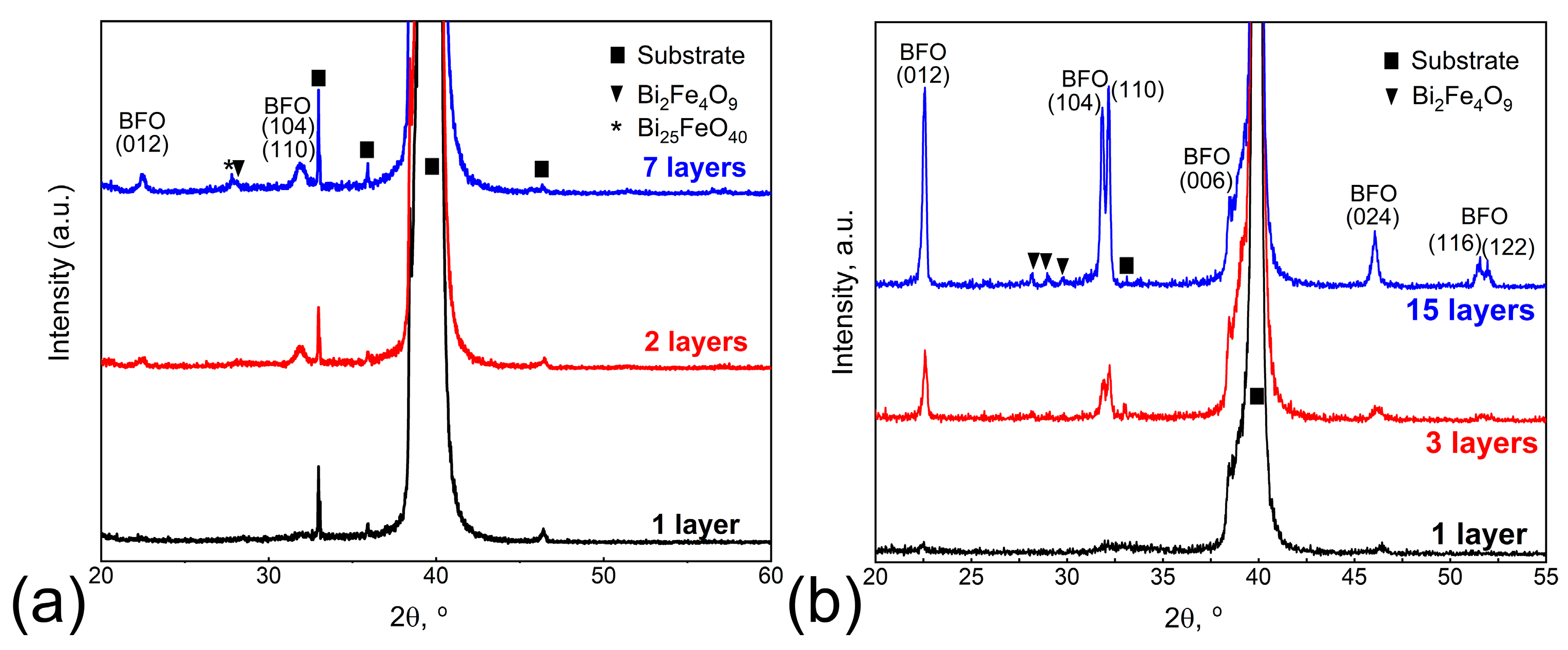
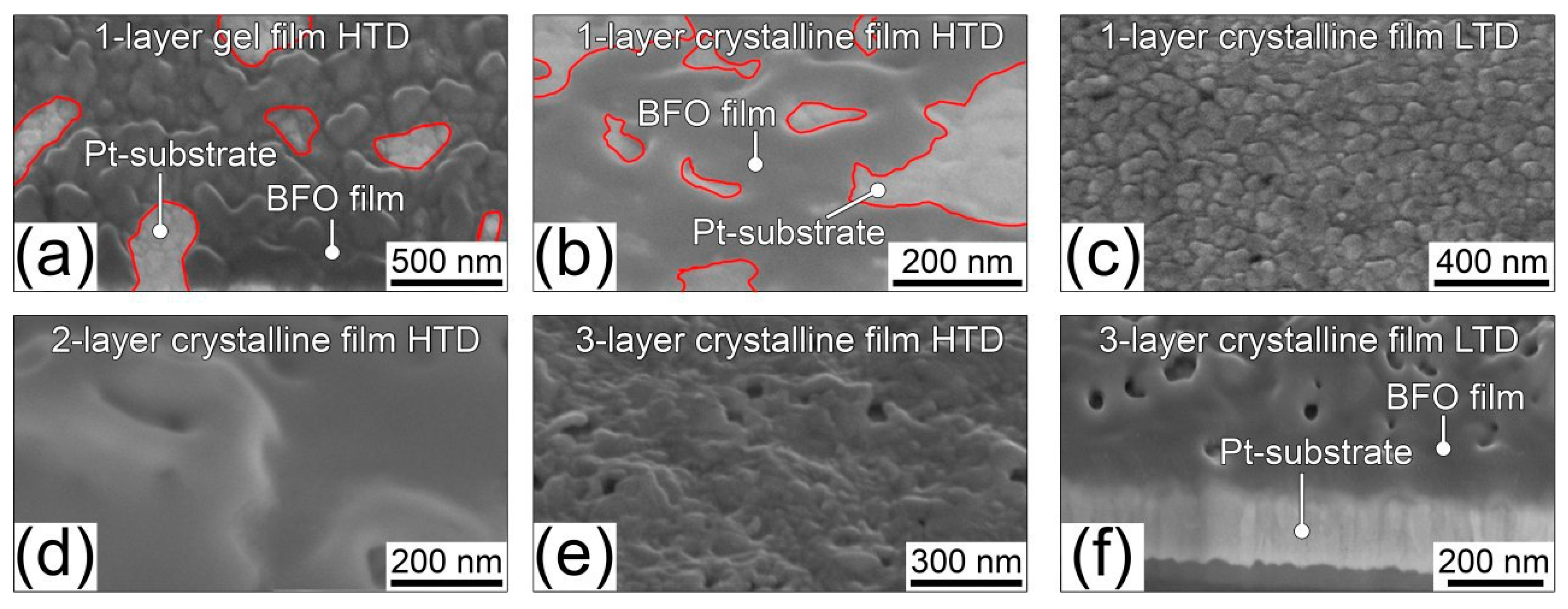
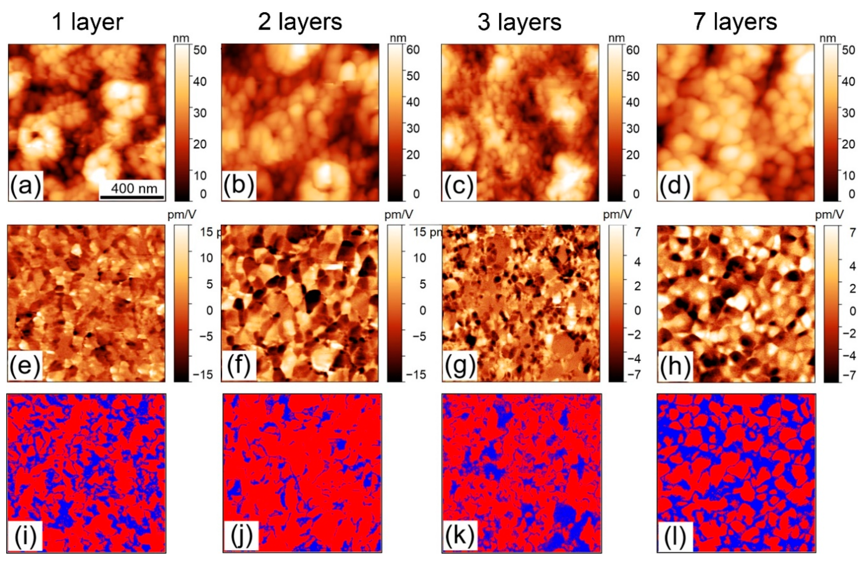
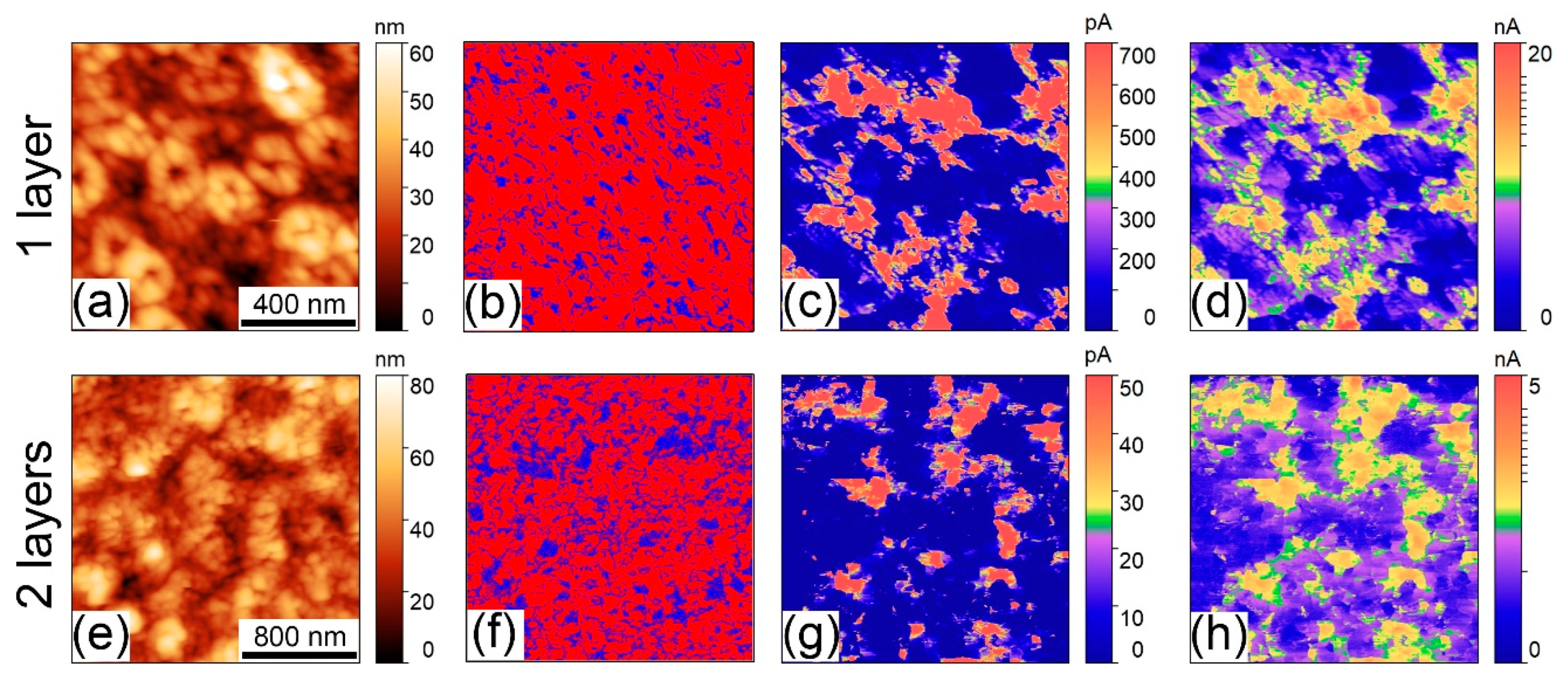
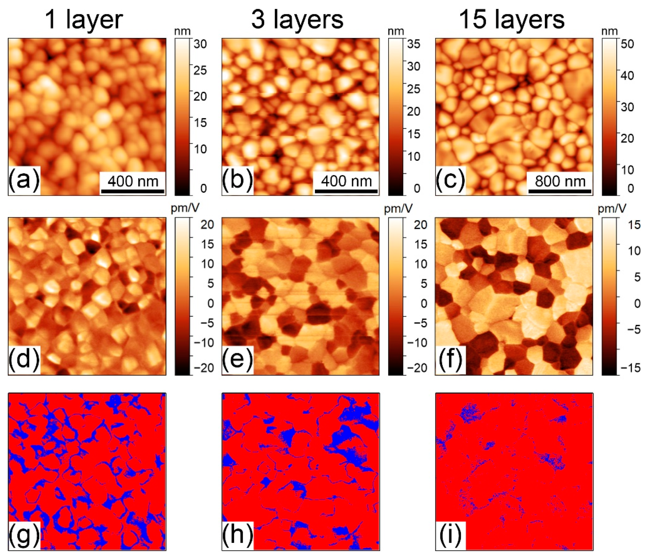
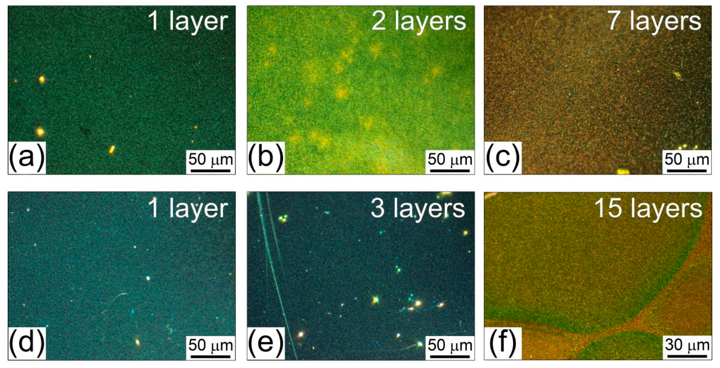
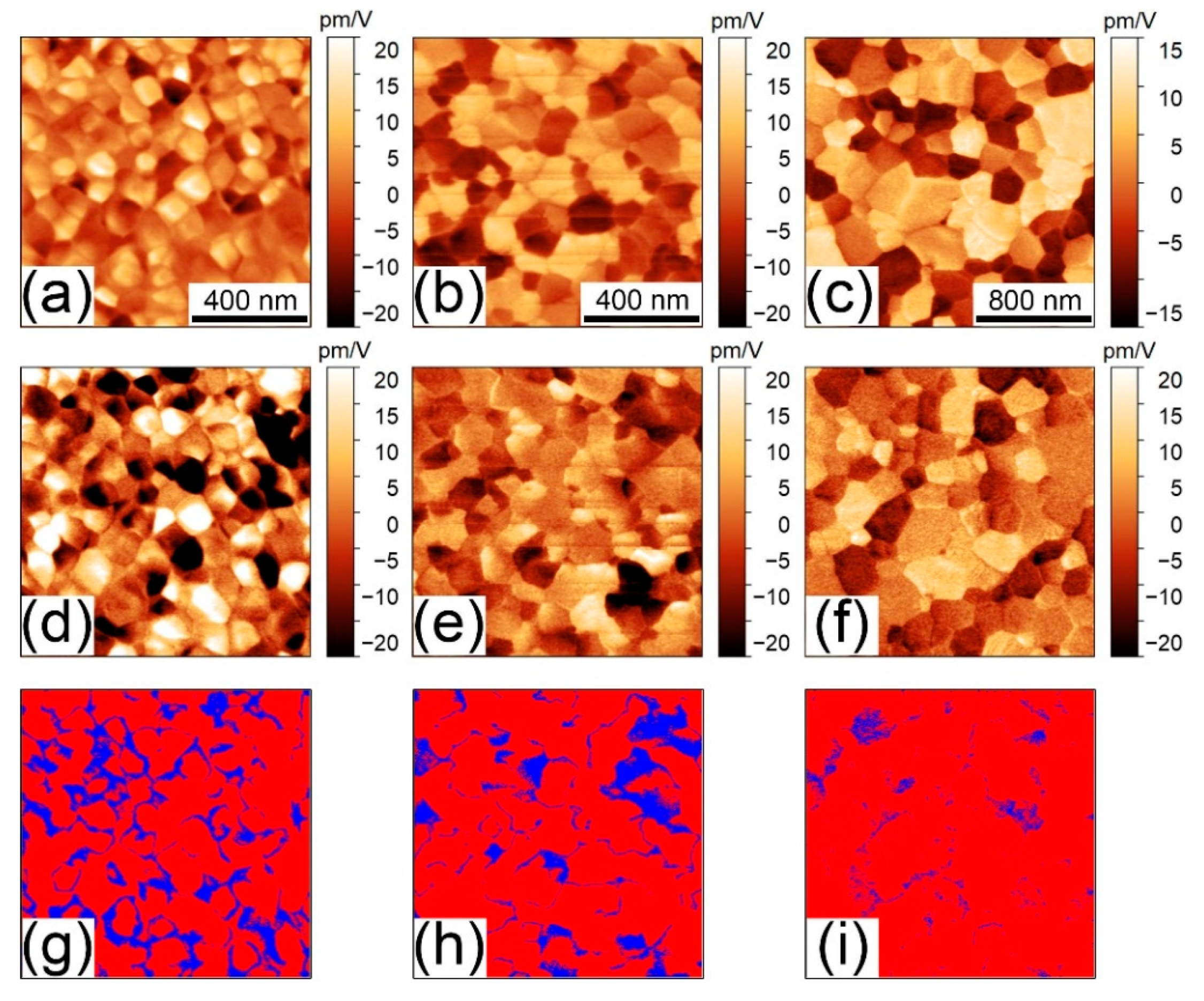
3. Results and Discussion

At the first step, XRD diffractograms of LTD and HTD sets of films with identical initial composition of the solution were compared (Figure 1). The perovskite BiFeO3 phase (ICDD [82-1254]) was observed in the films prepared with both drying conditions. LTD films revealed significantly better crystallinity visible in the resolved (104) and (110) reflexes (Figure 1b). These reflexes were overlapped in the HTD BFO films (Figure 1a). The analysis of XRD line broadening allowed estimating the average crystalline size to be about 25 nm in HTD series and 90–130 nm in the LTH series. The phase analysis showed a coexistence of the main BiFeO3 phase and secondary Bi2Fe4O9 and Bi25FeO40 phases: ICDD [82-1254], [72-1832], and [46-416] files, respectively. Bi25FeO40 secondary phase was found only in HTD films. The content of secondary phases in HTD films was quite large (up to 30 wt%), while LTD samples are nearly single-phase with the amount of the contaminants below 5 wt%.
The quality of the films at the large-scale was inspected by the optical microscopy (Figure A1 in Appendix A). The surface was quite homogeneous for all studied thicknesses except of the film with the large number of the layers: 10–15 deposited layers (500–750 nm). This can originate from the gradual decrease of the film quality caused by the sequential deposition of the layers. Nevertheless, the films were shown to be uniform enough for the representative local-scale studies with scanning electron microscopy (SEM). The material contrast between BFO and Pt substrate revealed by the in-lens detector allows clear distinction between the Pt substrate and the film [30] (Figure 2). It is seen that the HTD film deposited in one layer covers the substrate non-uniformly (Figure 2b). The coverage of the surface is an “island-like” with a fraction around 85%. The average thickness of the layer was estimated to be around 30–50 nm, which was measured with the atomic force microscopy from the step at the boundary of the islands. The coverage of the one-layer crystalline film, after 600 °C annealing treatment, was the same as for HTD gel film, after drying and before crystallization (Figure 2a). Oppositely, LTD-prepared films cover the substrate uniformly without any morphological features (Figure 2c). As the substrate preparation was identical for both sets of films, the difference in the BFO coverage can be attributed to the conditions of the drying procedure. Two- and three-layer films were homogeneous without extra inclusions (Figure 2d–f).
Topography of the HTD BFO films revealed a porous microstructure containing large-scale agglomerates of the grains, 100–200 nm, with small-scale 25–35 nm randomly-shaped grains inside them (Figure 3a–c). PFM measurements display the existence of the randomly distributed polarization across the grains of the films (light and dark contrast) and grains without piezoresponse (Figure 3e–h). Vertical PFM images are represented in Figure 3e–h, while lateral images can be found in Figure A2 (Appendix B). The calculated from PFM images distribution of the piezo-electrically active and inactive phase is shown in Figure 3i–l. The fractions of the phases are summarized in Table 1. As seen from the distribution images, piezoelectrically inactive phase in one and two-layer films is mainly concentrated in the vicinity of grain boundaries. The absence of the piezoresponse in these areas can be due to either segregated secondary phases or a large amount of defects. In three-layer films, distinct regions inside the grains without piezoresponse were observed which indicates secondary BFO phases, such as Bi4FeO9 identified in XRD diffractogram (Figure 1). The fraction of the non-polar phase in three-layer BFO films is higher by 10%–20% than in one- and two-layer films, which means the increase of the secondary phase concentration with thickness. The fractions extracted from PFM data fit well to those estimated from XRD.
To trace the effect of HTD microstructure on the leakage currents we studied a distribution of the local electric conductivity with the c-AFM method (Figure 4). The leakage was not spatially correlated with the position of the secondary phases. The leakage current maxima are coincident with the positions of the pores in one-layer films (Figure 4a–d). Moreover, the deposition of the additional layer does not completely prevent the leakage. It is clearly seen on the image with the logarithmic scale of the current (Figure 4h) that, in contrast to the one-layer film (Figure 4d), a noticeable leakage can be observed in the two-layer films in the places not correlated with the position of the pores. This indicates that the pores formed as a result of HTD procedure contribute to the macroscopic leakage current.
Interestingly, the film thickness also affects the value of the measured piezoelectric response of the films. The effective piezoelectric coefficient was estimated from the local measurements as an average value of the vertical piezoresponse amplitude divided by the applied AC voltage. One-layer and two-layer films yield similar values of the piezoelectric coefficient of about 3 pm/V (Table 1). Three-layer films revealed a reduction of the piezoelectric coefficient to 1.2 pm/V, which remains almost unchanged with increasing thickness. Local PFM measurements characterize mostly a contribution from the intrinsic mechanism of the piezoresponse and are exempted from the leakage through the pores and grain boundaries, domain wall [31], and hopping conductivity contribution to the piezoresponse [32,33]. This allows attributing the reduction of the piezoresponse to the crystalline quality of the BFO films that apparently reduces with increasing thickness.
Significantly different microstructure and piezoresponse distribution were found in the LTD series of the films (Figure 5). The lateral images can be found in Figure A3 (Appendix B). The topography of these films was smooth and independent on the number of deposited layers. The grain size was larger in LTD film in comparison to HTD: 70–110 nm having distinct faceted shapes that reveal the rhombohedral symmetry of pure BFO phase. An apparent absence of the piezoresponse was localized mostly in the grain boundary regions and a fraction of the piezoelectrically-inactive phase was gradually reduced with increasing thickness and achieved 95% in the thickest film (Table 2). This indicates a negligible amount of the secondary phases in a final film composition. Importantly, effective piezoelectric coefficient was larger in LTD films and reached 8.3 pm/V in three-layer films (Table 2). In the 15-layer 750 nm-thick film it was lower, which can be explained by the large increase of the film thickness that might change the distribution of the electric field under the atomic force microscope tip [34].
Further, we will discuss the apparent effect of the drying procedure in the CSD method on the overall functional properties of the films. BFO films were prepared from the mixture of the solvents and deposited with the spin coating method. It was shown that the morphology of the deposited layer is significantly dependent not only on the composition of the solution and following the crystallization procedure, but also on the drying conditions. The drying of the deposited films is known to determine the behavior of the gelation process [15,35]. It was shown that gelation occurs at temperatures higher than 70 °C [15]. We implemented a two-step procedure with, first, 10 min, at 80 °C and further at 300 °C, 5 min, (HTD) or 120 °C, 40 min (LTD) to complete the process. The drying of the gel is followed by the densification process caused by the capillary forces appearing as a consequence of the surface tension in the liquid phase [36]. Slow drying at 120 °C in LTD series of the films leads to gradual equilibrium evaporation of the solvent components and gel densification. Subsequent pyrolysis at 300 °C forms a homogeneous and relatively dense precursor film, which further crystallizes at 600 °C to the pure BiFeO3 phase. On the contrary, fast drying at 300 °C stimulates intensive boiling of the main gel components with the formation of the bubbles inside the film. That results in the capillary forces reduction accompanied by the formation of the porous micro-structure in the film. A faster nucleation rate at high temperature and the decrease of the gel local density led to a smaller grain size with worse grain interconnection. Hence, the BFO crystallization at 600 °C occurs slower and yields a smaller grain size and noticeable amount of the secondary phases in the final film. It should be noted that the problems of the deposition can be clearly distinguished only in the films with a small number of layers. Further deposition of the layers leads to the complete coverage of the substrate area. Nevertheless, the morphology of the initial layers is the most important because it influences subsequent deposition processes and the final micro-structure of the film. Larger grain size appears as a consequence of the low-temperature long-time gelation step, which provides better conditions for forming BFO films with the dense microstructure exhibiting better piezoelectric performance.

4. Conclusions

In summary, we performed the deposition of BiFeO3 thin films under different drying conditions that impact the effectiveness of the gelation step. The layer-by-layer control of the morphology, local piezoelectric response, and phase leakage current distribution was done by means of piezoresponse force microscopy and conductive atomic force microscopy methods. It was shown that the parameters of drying at the gelation steps of the BiFeO3 film preparation are important to produce high-quality and well-crystalline thin films across the large-scale area of the substrate. Long-time and low-temperature heating of the as-deposited solution in each layer of the film allows to achieve thick multi-layer films with 95 wt% of the main phase, larger grain size, and effective piezoelectric coefficient of about 5–8 pm/V. High temperature drying was demonstrated to be responsible for the deterioration of the initial layer coverage of the film and hampered chemical reactions leading to the formation of the small grain agglomerates with the large portion of the piezoelectrically inactive phases. Accumulated morphological changes during the deposition of the subsequent layers are responsible for the porosity and corresponding enhancement of the leakage current across the pores in the film bulk. As such, the demonstrated behavior addresses the importance of the gelation procedure for the final performance of the CSD BFO films and can explain many unsuccessful results in earlier reports. We believe that the demonstrated methodological approach can be useful for the improvement of the CSD pathway and development of good quality, large-scale BiFeO3 films.

Author Contributions

Methodology: V.S. (Vladislav Slabov), D.A., and A.V.; software: A.T.; investigation: A.A., A.S., D.M., and V.S. (Violetta Safina); resources: L.T., V.S. (Vladimir Shur), and A.K.; writing—original draft preparation: A.A. and D.M.; writing—review and editing: D.A., V.S. (Vladislav Slabov), A.S., and L.T.; visualization: A.A. and A.S.; supervision: D.A. and A.K.; project administration: D.A.; funding acquisition: D.A. All authors have read and agreed to the published version of the manuscript.

Funding

The research was funded by Russian Science Foundation, grant number 19-72-10076. The equipment of the Ural Center for Shared Use “Modern nanotechnology” UrFU was used.

Acknowledgments

The authors acknowledge Dmitry Karpinsky for the useful discussion.

Conflicts of Interest

The authors declare no conflict of interest.

Appendix A. Quality of the BFO Thin Films’ Coverage Inspected at the Large-Scale by Optical Microscopy

Figure A1. Dark field optical microscopy images of (ac) HTD and (df) LTD thin film BFO with different numbers of deposited layers.
Coatings 10 00438 g0a1

Appendix B. Vector PFM Images of the BFO Thin Films

Figure A2. PFM images and phase distribution images in: (a,e,i) one-layer; (b,f,j) two-layer; (c,g,k) three-layer; (d,h,l) seven-layer HTD BFO films. (ad) Vertical PFM images; (eh) lateral PFM images; (il) distribution of the piezoelectrically active (red) and non-active (blue) phases.
Coatings 10 00438 g0a2
Figure A3. PFM images and phase distribution images in: (a,d,g) one-layer; (b,e,h) three-layer; (c,f,i) 15-layer LTD BFO films. (ac) Vertical PFM images; (df) lateral PFM images; (gi) distribution of the piezoelectrically active (red) and non-active (blue) phases.
Coatings 10 00438 g0a3

References

  1. Catalan, G.; Scott, J.F. Physics and Applications of Bismuth Ferrite. Adv. Mater. 2009, 21, 2463–2485. [Google Scholar] [CrossRef]
  2. Fujino, S.; Murakami, M.; Anbusathaiah, V.; Lim, S.-H.H.; Nagarajan, V.; Fennie, C.J.; Wuttig, M.; Salamanca-Riba, L.; Takeuchi, I. Combinatorial discovery of a lead-free morphotropic phase boundary in a thin-film piezoelectric perovskite. Appl. Phys. Lett. 2008, 92, 202904. [Google Scholar] [CrossRef]
  3. Seidel, J.; Martin, L.W.; He, Q.; Zhan, Q.; Chu, Y.-H.; Rother, A.; Hawkridge, M.E.; Maksymovych, P.; Yu, P.; Gajek, M.; et al. Conduction at domain walls in oxide multiferroics. Nat. Mater. 2009, 8, 229–234. [Google Scholar] [CrossRef] [PubMed] [Green Version]
  4. Rojac, T.; Ursic, H.; Bencan, A.; Malic, B.; Damjanovic, D. Mobile Domain Walls as a Bridge between Nanoscale Conductivity and Macroscopic Electromechanical Response. Adv. Funct. Mater. 2015, 25, 2099–2108. [Google Scholar] [CrossRef]
  5. Morozovska, A.N.; Vasudevan, R.K.; Maksymovych, P.; Kalinin, S.V.; Eliseev, E.A. Anisotropic conductivity of uncharged domain walls in BiFeO. Phys. Rev. B 2012, 86, 085315. [Google Scholar] [CrossRef] [Green Version]
  6. Tra, V.T.; Yang, J.-C.; Hsieh, Y.-H.; Lin, J.-Y.; Chen, Y.-C.; Chu, Y.-H. Controllable electrical conduction at complex oxide interfaces. Phys. Status Solidi—Rapid Res. Lett. 2014, 8, 478–500. [Google Scholar] [CrossRef]
  7. Meier, D. Functional domain walls in multiferroics. J. Phys. Condens. Matter 2015, 27, 463003. [Google Scholar] [CrossRef] [PubMed]
  8. Maksymovych, P.; Morozovska, A.N.; Yu, P.; Eliseev, E.A.; Chu, Y.H.; Ramesh, R.; Baddorf, A.P.; Kalinin, S.V. Tunable metallic conductance in ferroelectric nanodomains. Nano Lett. 2012, 12, 209–213. [Google Scholar] [CrossRef]
  9. Yin, K.; Li, M.; Liu, Y.; He, C.; Zhuge, F.; Chen, B.; Lu, W.; Pan, X.; Li, R.-W. Resistance switching in polycrystalline BiFeO3 thin films. Appl. Phys. Lett. 2010, 97, 042101. [Google Scholar] [CrossRef]
  10. Wang, J.; Neaton, J.B.; Zheng, H.; Nagarajan, V.; Ogale, S.B.; Liu, B.; Viehland, D.; Vaithyanathan, V.; Schlom, D.G.; Waghmare, U.V.; et al. Epitaxial BiFeO3 multiferroic thin film heterostructures. Science 2003, 299, 1719–1722. [Google Scholar] [CrossRef]
  11. Li, J.; Wang, J.; Wuttig, M.; Ramesh, R.; Wang, N.; Ruette, B.; Pyatakov, A.P.; Zvezdin, A.K.; Viehland, D. Dramatically enhanced polarization in (001), (101), and (111) BiFeO3 thin films due to epitiaxial-induced transitions. Appl. Phys. Lett. 2004, 84, 5261–5263. [Google Scholar] [CrossRef] [Green Version]
  12. Das, R.R.; Kim, D.M.; Baek, S.H.; Eom, C.B.; Zavaliche, F.; Yang, S.Y.; Ramesh, R.; Chen, Y.B.; Pan, X.Q.; Ke, X.; et al. Synthesis and ferroelectric properties of epitaxial BiFeO3 thin films grown by sputtering. Appl. Phys. Lett. 2006, 88, 242904. [Google Scholar] [CrossRef]
  13. Kartavtseva, M.S.; Gorbenko, O.Y.; Kaul, A.R.; Murzina, T.V.; Savinov, S.A.; Barthélémy, A. BiFeO3 thin films prepared using metalorganic chemical vapor deposition. Thin Solid Films 2007, 515, 6416–6421. [Google Scholar] [CrossRef]
  14. Yang, B.; Jin, L.; Wei, R.; Tang, X.; Hu, L.; Tong, P.; Yang, J.; Song, W.; Dai, J.; Zhu, X.; et al. Chemical Solution Route for High-Quality Multiferroic BiFeO3 Thin Films. Small 2019, 3, 1903663. [Google Scholar] [CrossRef] [Green Version]
  15. Zhang, Q.; Sando, D.; Nagarajan, V. Chemical route derived bismuth ferrite thin films and nanomaterials. J. Mater. Chem. C 2016, 4, 4092–4124. [Google Scholar] [CrossRef]
  16. Rojac, T.; Bencan, A.; Malic, B.; Tutuncu, G.; Jones, J.L.; Daniels, J.E.; Damjanovic, D. BiFeO3 Ceramics: Processing, Electrical, and Electromechanical Properties. J. Am. Ceram. Soc. 2014, 97, 1993–2011. [Google Scholar] [CrossRef]
  17. Valant, M.; Axelsson, A.; Alford, N.; Bifeo, P. Peculiarities of a Solid-State Synthesis of Multiferroic Polycrystalline BiFeO Peculiarities of a Solid-State Synthesis of Multiferroic. Chem. Mater. 2007, 19, 5431–5436. [Google Scholar] [CrossRef]
  18. Schrade, M.; Masó, N.; Perejón, A.; Pérez-Maqueda, L.A.; West, A.R. Defect chemistry and electrical properties of BiFeO3. J. Mater. Chem. C 2017, 5, 10077–10086. [Google Scholar] [CrossRef] [Green Version]
  19. Zha, J.; Roggendorf, H. Sol-Gel Science, the Physics and Chemistry of Sol-Gel Processing; Brinker, C.J., Scherer, G.W., Eds.; Academic Press: Boston, MA, USA, 1990. [Google Scholar]
  20. Nakamura, Y.; Nakashima, S.; Okuyama, M. Improvement of ferroelectric properties of BiFeO3 thin films by postmetallization annealing and electric field application. J. Appl. Phys. 2009, 105, 061616. [Google Scholar] [CrossRef]
  21. Nakamura, Y.; Nakashima, S.; Okuyama, M. Influences of Surface Texture and Bi/Fe Ratio on Electric Properties of BiFeO3 Thin Films Prepared by Chemical Solution Deposition. Jpn. J. Appl. Phys. 2008, 47, 7250–7253. [Google Scholar] [CrossRef]
  22. Zhang, Q.; Valanoor, N.; Standard, O. Chemical solution deposition derived (001)-oriented epitaxial BiFeO3 thin films with robust ferroelectric properties using stoichiometric precursors (invited). J. Appl. Phys. 2014, 116, 066810. [Google Scholar]
  23. William, R.V.; Marikani, A.; Madhavan, D. Dielectric behavior and magnetical response for porous BFO thin films with various thicknesses over Pt/Ti/SiO2/Si substrate. Ceram. Int. 2016, 42, 6807–6816. [Google Scholar] [CrossRef]
  24. Jungk, T.; Hoffman, Á.; Soergel, E. Consequences of the background in piezoresponse force microscopy on the imaging of ferroelectric domain structures. J. Microsc. 2007, 227, 72–78. [Google Scholar] [CrossRef] [PubMed]
  25. Seol, D.; Kim, B.; Kim, Y. Non-piezoelectric effects in piezoresponse force microscopy. Curr. Appl. Phys. 2017, 17, 661–674. [Google Scholar] [CrossRef] [Green Version]
  26. Alikin, D.; Slautin, B.; Abramov, A.; Rosato, D.; Shur, V.; Tselev, A.; Kholkin, A. Kholkin Correlative Confocal Raman and Scanning Probe Microscopy in the Ionically Active Particles of LiMn2O4 Cathodes. Materials 2019, 12, 1416. [Google Scholar] [CrossRef] [PubMed] [Green Version]
  27. Balke, N.; Jesse, S.; Yu, P.; Carmichael, B.; Kalinin, S.V.; Tselev, A. Quantification of surface displacements and electromechanical phenomena via dynamic atomic force microscopy. Nanotechnology 2016, 27, 425707. [Google Scholar] [CrossRef]
  28. Alikin, D.O.; Abramov, A.S.; Kosobokov, M.S.; Gimadeeva, L.V.; Romanyuk, K.N.; Slabov, V.; Shur, V.Y.; Kholkin, A.L. Calibration of the in-plane PFM response by the lateral force curves. Ferroelectrics 2020. accepted. [Google Scholar] [CrossRef]
  29. Alikin, D.O.; Turygin, A.P.; Walker, J.; Rojac, T.; Shvartsman, V.V.; Shur, V.Y.; Kholkin, A.L. Quantitative phase separation in multiferroic Bi0.88Sm0.12FeO3 ceramics via piezoresponse force microscopy. J. Appl. Phys. 2015, 118, 072004. [Google Scholar] [CrossRef]
  30. Nagoshi, M.; Aoyama, T.; Sato, K. Extraction of topographic and material contrasts on surfaces from SEM images obtained by energy filtering detection with low-energy primary electrons. Ultramicroscopy 2013, 124, 20–25. [Google Scholar] [CrossRef]
  31. Wada, S.; Yako, K.; Kakemoto, H.; Tsurumi, T.; Kiguchi, T. Enhanced piezoelectric properties of barium titanate single crystals with different engineered-domain sizes. J. Appl. Phys. 2005, 98, 014109. [Google Scholar] [CrossRef]
  32. Morozov, M.I.; Einarsrud, M.A.; Grande, T. Atmosphere controlled conductivity and Maxwell-Wagner relaxation in Bi0.5K0.5TiO3—BiFeO3 ceramics. J. Appl. Phys. 2014, 115, 044104. [Google Scholar] [CrossRef] [Green Version]
  33. Morozov, M.I.; Damjanovic, D. Charge migration in Pb(Zr,Ti)O3 ceramics and its relation to ageing, hardening, and softening. J. Appl. Phys. 2010, 107, 1–10. [Google Scholar] [CrossRef] [Green Version]
  34. Soergel, E. Piezoresponse force microscopy (PFM). J. Phys. D. Appl. Phys. 2011, 44, 464003. [Google Scholar] [CrossRef]
  35. Muresan, L.M. Corrosion Protective Coatings for Ti and Ti Alloys Used for Biomedical Implants. In Intelligent Coatings for Corrosion Control; Elsevier: Amsterdam, The Netherlands, 2015; pp. 585–602. ISBN 9780124115347. [Google Scholar]
  36. Lecloux, A.; Pirard, J. High-temperature catalysts through sol–gel synthesis. J. Non. Cryst. Solids 1998, 225, 146–152. [Google Scholar] [CrossRef]
Figure 1. XRD diffractograms of the (a) HTD and (b) LTD BFO thin films with different numbers of the layers.
Coatings 10 00438 g001
Figure 2. In-lens SEM images of BFO thin films: (a) HTD one-layer gel film, (b) HTD one-layer crystalline film, (c) LTD one-layer crystalline film, (d) HTD two-layer crystalline film, and (e) HTD three-layer crystalline film. (f) Cross-section of the HTD three-layer crystalline film done by focused ion beam etching. Red line depicts boundary of the BFO “islands”.
Coatings 10 00438 g002
Figure 3. PFM images and phase distribution images in: (a,e,i) one-layer; (b,f,j) two-layer; (c,g,k) three-layer; (d,h,l) seven-layer HTD BFO films. (ad) Topography; (eh) vertical PFM images; (il) distribution of the piezoelectrically-active (red) and non-active (blue) phases.
Coatings 10 00438 g003
Figure 4. C-AFM measurements of the leakage current in (ad) one-layer; (bh) two-layer HTD BFO films. (a,e) Topography; (b,f) distribution of the piezoelectrically active (red) and non-active (blue) phases; (c,g) electrical current; (d,h) electrical current with logarithmic vertical scale.
Coatings 10 00438 g004
Figure 5. PFM images and phase distribution images in: (a,d,g) one-layer; (b,e,h) three-layer; (c,f,i) 15-layer LTD BFO films. (ac) Topography; (df) vertical PFM images; (gi) distribution of the piezoelectrically-active (red) and non-active (blue) phases.
Coatings 10 00438 g005
Table 1. Phase distribution and piezoelectric coefficient for the HTD BFO thin films as a function of thickness.
ThicknessOne LayerTwo LayersThree LayersSeven Layers
Polar phase75%86%67%65%
Non-polar phase25%14%33%35%
Effective piezoelectric coefficient2.5 ± 1.0 pm/V3. 5± 1.5 pm/V1.2 ± 0.8 pm/V1.3 ± 0.3 pm/V
Table 2. Phase distribution and piezoelectric coefficient for the LTD BFO thin films depending on thickness.
Thickness1 Layer3 Layers15 Layers
Polar phase76%87%95%
Non-polar phase24%13%5%
Effective piezoelectric coefficient3.5 ± 0.8 pm/V8.3 ± 1.6 pm/V5.4 ± 1.6 pm/V

