1. Introduction
Transparent conductive oxide (TCO) thin films possess excellent conductivity and optical transmittance in the visible and near-infrared regions, and are thus applied in many photoelectric components nowadays, including solar cells [
1,
2], organic light-emitting diodes [
3,
4], thin-film transistors [
5,
6], photovoltaic batteries [
7,
8,
9], electrochromic devices [
10,
11,
12], and tablet displays [
13,
14,
15,
16]. Metallic films are generally opaque in the visible light range. However, for film thicknesses of less than 100 Å, visible light is transmitted through the film, while infrared (IR) light is reflected. Moreover, for metals such as In
2O
3, ZnO, SnO
2, TiO
2, and CdO with energy gaps of 3 eV or more, the film also has excellent semiconducting properties [
17].
The literature contains many studies on the optoelectronic properties of metallic films [
18,
19,
20]. In addition, various authors have investigated the properties of three-layer TCO films with oxide/metal/oxide or metallic oxide/metal/metallic oxide structures [
21]. The results have shown that such films not only suppress the reflection from the metallic layer in the visible light range but also produce a transmittance effect [
22,
23]. Consequently, the TCO thin films are used in solar cells, gas sensors, LCD displays, etc.
Among the various metal oxides in common use nowadays, SnO
2 has poorer electrical properties than ITO, but a superior photoelectric performance in the IR region. Furthermore, SnO
2 has good chemical and thermal stability and is also amenable to surface modification in order to expand its working wavelength range. As a result, SnO
2 conductive films are widely used for such applications as gas sensors, solar energy battery electrodes, low-radiation glasses, etc. [
24,
25]. However, SnO
2 films are less easily used in tablet display applications due to their high electrical resistance and poor etching effect.
Accordingly, the present study explores the feasibility of improving the optical and electrical properties of SnO
2 thin films by doping the films with Ti. Note that Ti is deliberately selected as the dopant material here, since it has a maximum chemical valence of +4 [
26], where the radius of Ti
4+ is 0.0605 nm, while that of Sn
4+ is 0.069 nm. Due to the similarity of the ion radii, the Ti
4+ ions readily replace the Sn
4+ ions in the crystal lattice of the SnO
2 and hence modify its electrical and optical behavior. The Ti:SnO
2 films are deposited on glass substrates using a radio frequency (RF) magnetron sputtering system and then are annealed at various temperatures in the range of 200–500 °C to prompt the diffusion of the Ti atoms into the SnO
2 layer. The optoelectronic properties of the films are then systematically explored in order to determine the annealing temperature, which results in the optimal tradeoff between the electrical and optical properties of the film, respectively.
2. Experimental Procedure
The glass plate was purchased from Corning company (Corning, NY, USA) and cut into pieces the size of 25 mm × 25 mm × 7 mm (length × width × thickness) using a diamond saw. The substrates were cleaned sequentially in deionized (DI) water, acetone, and IPA (isopropanol), and DI water once again in order to remove any pollutants, residual solvents, or nonorganic components from the substrate surface. The substrates were then dried in an oven at 90 °C until the water was completely vaporized. The thin films were prepared using a sputtering target (two-inch diameter) composed of SnO2(95%) and TiO2(5%). The Ti:SnO2 films were then deposited on the glass substrates using an RF sputtering system with a sputtering power of 60 W, an argon gas flow rate of 29 sccm, an oxygen flow rate of 1 sccm, and a bias of 7.5 mTorr. The sputtering process was performed without substrate heating. The purpose of this experiment was to study the impact of different process parameters and conditions on the characteristics of a transparent conductive film. Following the deposition process, the Ti:SnO2 films were annealed at temperatures of 200, 300, 400, and 500 °C for 30 min. The structures of the annealed thin films were examined by X-ray diffraction (XRD, Bruker, Billerica, MA, USA). In addition, the surface roughness and crystal size were determined by atomic force microscopy (AFM, NTMDT-AFM, Bruker, Billerica, MA, USA) and scanning electron microscopy (SEM, JEOL JSM-7000F, JEOL, Kyoto, Janpan), respectively. The photoelectric property data consisted of light transmittance, resistivity, carrier concentration by spectrophotometer (UV Spectrophotometer, Hitachi 2900, Hitachi, Tokyo, Japan), and a Hall measuring instrument(AHM-800B, Advnaced Design Technology, Taipei, Taiwan), respectively. In this paper, the measurement for each condition was performed six times to confirm the data.
3. Results and Discussion
3.1. Effects of Annealing Temperature on Ti:SnO2 Film Thickness
Table 1 shows the thickness of the various Ti:SnO
2 films, measured by alpha–step profilometer (KLA-Tencor, Milpitas, CA, USA). In general, it is noted that while the annealing temperature has no significant effect on the film thickness, the thickness increases slightly in the film annealed at 200 °C but then reduces progressively as the annealing temperature is further increased to 500 °C.
3.2. Effects of Annealing Temperature on Structural Properties of Ti:SnO2 Films
Figure 1 shows the XRD patterns of the as-deposited and annealed Ti:SnO
2 thin films. As the annealing temperature increases, prominent peaks are observed at 26.6°, 33.8°, and 51.7° corresponding to (110), (101), and (211) phases, respectively. The (101) phase is a combined SnO and SnO
2 phase [
27]; some of the Sn and Ti atoms are replaced by a diffused process following the annealing process [
28,
29]. Notably, diffraction peaks are very small in the as-deposited film or the film annealed at 200 °C. However, as the annealing temperature increases to 300 °C, the crystalline phase appears more within the film. The crystalline structure becomes increasingly pronounced as the annealing temperature increases to 500 °C, and hence has a significant effect on the electrical and optical properties, as described in the following sections.
3.3. Effects of Annealing Temperature on Electrical Resistivity
Figure 2 shows the electrical properties of the as-deposited and annealed Ti:SnO
2 films. Previous studies have shown that the TCO transmission mechanism is governed mainly by element doping and oxygen vacancies [
29,
30]. For the Ti:SnO
2 thin films considered in the present study, the oxygen vacancy contributes two free electrons, and therefore dominates the transmission mechanism. Although the Sn
+ atom also provides a free electron, it cannot be activated as effectively as the oxygen vacancy because the carrier concentration is primarily controlled by the oxygen vacancy. As described above, the Ti:SnO
2 film has a small crystal structure in the as-deposited condition and under an annealing temperature of 200 °C. However, as the annealing temperature is increased to 300 °C, the film has a low resistivity of 5.65 × 10
−3 Ω·cm as a result of the high carrier concentration. Meantime, as the annealing temperature is increased beyond 300 °C, the SnO and SnO
2 combined phase are gradually formed, causing the carrier concentration to decrease and the resistivity to increase.
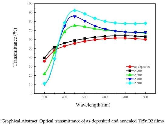
3.4. Transmittance
Figure 3 shows the optical transmittance properties of the various Ti:SnO
2 thin films. For the as-deposited film, the mean transmittance has a low value of approximately 58% due to the poor effect of the replaced Sn for the Ti atom. However, the transmittance improves significantly in the annealed samples, particularly in those annealed at temperatures of 300 °C or more. In conventional ITO films, the optical energy gap theoretically increases as the carrier concentration increases, since the Fermi level moves into the conduction band and the electrons on the valence band are forced to jump to the conduction band, thereby requiring more energy and resulting in the so-called Burstein–Moss effect [
31,
32]. However, the optical energy gap rises with a decreasing carrier concentration. Such a phenomenon may be due to an interaction effect between ion compounds. For example, Zn
2+ and Sn
4+ ions coexist in IZTO films and trigger the generation of a donor-accepter pair, which reduces the energy gap and mitigates the Burstein–Moss effect. For the present Ti:SnO
2 films, the carrier concentration decreases following annealing at temperatures higher than 200 °C (see
Figure 2). However, the energy gap and mean transmittance both increase (see
Table 2 and
Figure 3, respectively). For an annealing temperature of 200 °C, the improvement in the transmittance is very modest (i.e., from around 58% for the as-deposited sample to approximately 60% for the annealed sample). However, for an annealing temperature of 300 °C, the film undergoes a transformation from a homogenous crystalline structure and the mean transmittance improves to almost 75%. Furthermore, as the annealing temperature increases, the transformation toward a crystalline structure becomes more complete (see
Figure 1) and hence the mean transmittance increases. Thus, the film annealed at a temperature of 500 °C shows the maximum mean transmittance of approximately 74.2%.
Figure 4 shows the relationship between the optical absorption coefficient (α) and photon energy(
hν) for the Ti:SnO
2 film. The optical band gap (
Eg) is calculated as follows with the equation [
33,
34]:
where α is the absorption coefficient, ν is the frequency of incident light, h is the Planck’s constant, and
A is constant. The optical band gap is extrapolating the straight-line portion of the plot to the energy axis.
Table 2 shows the calculated values of the optical band gap for the present Ti:SnO
2 thin films. Furthermore, an Eg value greater than 3 eV is regarded as excellent. Referring to
Table 2, the Eg value of the present Ti:SnO
2 films increases with an increase in annealing temperature and is equal to 3.28 eV at an annealing temperature of 500 °C. Moreover, an Eg value greater than 3 eV is obtained for all of the films annealed at a temperature of 300 °C or more.
3.5. Surface Feature Analysis
Figure 5 and
Figure 6 show AFM and SEM images of the various as-deposited and annealed Ti:SnO
2 films. The mean surface roughness values of the films are listed in
Table 3. As shown, the as-deposited sample has a surface roughness of 0.31 nm. However, following annealing at 300 °C, the surface roughness falls to a value of around 0.35 nm due to the formation of the crystalline phase. However, as the annealing temperature is further increased, the surface roughness reduces and has a value of just 0.296 nm in the sample processed at the highest annealing temperature of 500 °C. The AFM and SEM images show that the as-deposited Ti:SnO
2 film and the film annealed at 300 °C have higher surface roughness. Annealing at a temperature of 300 °C results in high roughness, but after 300 °C the roughness is decreased.
3.6. Effects of Annealing Temperature on Crystal Size
The full width at half maximum (FWHM) values of the peaks in the XRD patterns can be derived from the following Scherrer formula [
35]:
where
D is the grain size, β is the XRD peak FWHM, λ is the wavelength of the incident light, and θ is the diffraction angle of the incident light. In the XRD process, λ and θ have constant values. Consequently, the grain size,
D, and FWHM, β, are inversely related. (Cullity and Stock 2001).
Figure 7 shows the FWHM and crystal grain size values of the present Ti:SnO
2 films. Note that the as-deposited film has a small crystal structure, and hence the FWHM and crystal size values are also calculated carefully. However, for an annealing temperature of 300 °C, the Ti:SnO
2 film has a crystalline structure with a grain size of around 14.89 nm. As the annealing temperature is increased, the crystalline structure becomes more pronounced. Consequently, the grain size decreases, while the FWHM increases. For the maximum annealing temperature of 500 °C, the grain size is equal to approximately 11.56 nm, while the FWHM increases to 0.8.
3.7. Figure of Merit(ΦTC)
The figure of merit (Φ
TC) is an important factor used to evaluate the performance of TCO films from the relationship between transmittance and electrical properties. The figure of merit (Φ
TC) is defined as [
36] as follows:
where
T is the average optical transmittance, and
Rsh is the sheet resistance of the films.
Table 4 shows the figure of merit(Φ
TC) results for the as-deposited and annealed Ti:SnO
2 thin films. As shown, the optimal Φ
TC (3.99 × 10
−4 Ω
−1) is obtained at an annealing temperature of 500 °C. According to the figure, we see that because of an insignificant difference in electrical properties, it has led to a more obvious influence on quality elements from mean optical transmittance, and the optimal mean transmittance is seen at 500 °C. Therefore, optimum quality elements can be achieved at 500 °C.
3.8. Comparison of Other Methods to the Ti-Doped SnO2 Method
Table 5 shows some literature about the Ti-doped SnO
2 thin film under different methods (e.g., sol-gel and ultrasonic spray). We listed the optical and electrical properties in
Table 5 from the literature and this study. From
Table 5, it can be seen that the RF sputter method has some better optical and electrical properties than sol-gel. However, the cost of the sputtering method is more expansive.
4. Conclusions
This study has examined the electrical and optical properties of Ti:SnO2 thin films deposited on glass substrates and then annealed at temperatures ranging from 200–500 °C. The experimental results have shown that the thickness of the Ti:SnO2 films is insensitive to the annealing temperature. However, as the annealing temperature increases, strong peaks in the XRD patterns emerge corresponding to (110), (101), and (211) phases. Hence, it is inferred that the films increase a well-crystalline structure at higher annealing temperatures. The Ti:SnO2 film annealed at the lowest temperature of 300 °C shows both the minimum resistivity of 5.65 × 10⁻³ Ω·cm. The energy gap and optical transmittance both increase with increasing annealing temperature and have values of 3.28 eV and 74.2% at an annealing temperature of 500 °C. The AFM results show that for the samples annealed at temperatures of more than 300 °C, the mean surface roughness reduces with an increase in annealing temperature. The SEM observations suggest that the lower surface roughness is the result of larger grain size. In particular, the grain size decreases from 14.89 nm in the film annealed at 300 °C to 11.56 nm in the film annealed at 500 °C. The Ti:SnO2 film annealed at a temperature of 500 °C shows the highest ΦTC of 3.99 × 10⁻⁴ Ω−1. The characterization results have suggested that the optimal performance of this film is due to optical transmittance.
Author Contributions
Data curation—formal analysis, C.-F.L. and Y.-S.H.; Writing—Original draft preparation— methodology—investigation T.-H.C.; Review and editing—investigation C.-H.K. All authors have read and agreed to the published version of the manuscript.
Funding
This research was funded by the Ministry of Science and Technology, Taipei, Taiwan, under Grant No. 106-2628-E-992 -302 -MY3.
Acknowledgments
The authors gratefully acknowledge the financial support provided to this study by the Ministry of Science and Technology.
Conflicts of Interest
The authors declare no conflict of interest.
References
- Fleischer, K.; Arca, E.; Shvets, I.V. Improving solar cell efficiency with optically optimised TCO layers. Sol. Energy Mater. Sol. Cells 2012, 101, 262–269. [Google Scholar] [CrossRef] [Green Version]
- Sun, W.; Wang, S.; Li, S.; Miao, X.; Zhu, Y.; Du, C.; Ma, R.; Wang, C. Reactive-Sputtered Prepared Tin Oxide Thin Film as an Electron Transport Layer for Planar Perovskite Solar Cells. Coatings 2019, 9, 320. [Google Scholar] [CrossRef] [Green Version]
- Oh, M.; Seo, I. Enhanced performance of GaN-based green light-emitting diodes with gallium-doped ZnO transparent conducting oxide. J. Electron. Mater. 2014, 43, 1232–1236. [Google Scholar] [CrossRef]
- Najafi, N.; Rozati, S.M. Structural and Electrical Properties of SnO2:F Thin Films Prepared by Chemical Vapor Deposition Method. Acta Phys. Pol. A 2017, 131, 222–225. [Google Scholar] [CrossRef]
- Jang, B.; Kim, T.; Lee, S.; Lee, W.Y.; Kang, H.; Cho, C.S.; Jang, J. High Performance Ultrathin SnO2 Thin-Film Transistors by Sol–Gel Method. IEEE Electron Device Lett. 2018, 39, 1179–1182. [Google Scholar] [CrossRef]
- Presley, R.E.; Munsee, C.L.; Park, C.H.; Hong, D.; Wager, J.F.; Keszler, D.A. Tin oxide transparent thin-film transistors. J. Phys D Appl. Phys. 2004, 37, 2810–2813. [Google Scholar] [CrossRef] [Green Version]
- Kim, C.; Noh, M.; Choi, M.; Cho, J.; Park, B. Critical size of a nano SnO2 electrode for Li secondary battery. Chem. Mater. 2005, 17, 3297–3301. [Google Scholar] [CrossRef]
- Riveros, R.; Romero, E.; Gordillo, G. Synthesis and Characterization of Highly Transparent and Conductive SnO2:F and In2O3:Sn thin Films Deposited by Spray Pyrolysis. Braz. J. Phys. 2006, 36, 1042–1045. [Google Scholar] [CrossRef] [Green Version]
- Haider, A.J.; Mohammed, A.J.; Shaker, S.S.; Yahya, K.Z.; Haider, M.J. Sensing Characteristics of Nanostructured SnO2 Thin Films as Glucose sensor. Energy Procedia 2017, 119, 473–481. [Google Scholar] [CrossRef]
- Patil, P.S.; Sadale, S.B.; Mujawar, S.H.; Shinde, P.S.; Chigare, P.S. Synthesis of electrochromic tin oxide thin films with faster response by spray pyrolysis. Appl. Sur. Sci. 2007, 253, 8560–8567. [Google Scholar] [CrossRef]
- Chang, J.Y.; Chen, Y.C.; Wang, C.M.; Chen, Y.W. Electrochromic Properties of Li-Doped NiO Films Prepared by RF Magnetron Sputtering. Coatings 2020, 10, 87. [Google Scholar] [CrossRef] [Green Version]
- Vernardou, D. Using an Atmospheric Pressure Chemical Vapor Deposition Process for the Development of V2O5 as an Electrochromic Material. Coatings 2017, 7, 24. [Google Scholar] [CrossRef] [Green Version]
- Isono, T.; Fukuda, T.; Nakagawa, K.; Usui, R.; Satoh, R.; Morinaga, E.; Mihara, Y. Highly conductive SnO2thin films for flat-panel displays. J. Soc. Inf. Disp. 2007, 15, 161–166. [Google Scholar] [CrossRef]
- Patel, P.; Karmakar, A.; Jariwal, C.; Ruparelia, J.P. Preparation and Characterization of SnO2 Thin Film Coating using rf-Plasma Enhanced Reactive Thermal Evaporation. Procedia Eng. 2013, 51, 473–479. [Google Scholar] [CrossRef] [Green Version]
- Haider, A.J.; Shaker, S.S.; Mohammed, A.H. A Study of Morphological, Optical and Gas Sensing Properties for Pure and Ag Doped SnO2 Prepared by Pulsed Laser Deposition (PLD). Energy Procedia 2013, 36, 776–787. [Google Scholar] [CrossRef] [Green Version]
- Lee, S.H.; Kwon, K.; Kim, K.; Yoon, J.S.; Choi, D.S.; Yoo, Y.; Kim, C.; Kang, S.; Kim, J.H. Electrical, Structural, Optical, and Adhesive Characteristics of Aluminum-Doped Tin Oxide Thin Films for Transparent Flexible Thin-Film Transistor Applications. Materials 2019, 12, 137. [Google Scholar] [CrossRef] [Green Version]
- Shanthi, E.; Banerjee, A.; Dutta, V.; Chopra, K.L. Electrical and optical properties of tin oxide films doped with F and (Sb + F). J. Appl. Phys. 1982, 53, 1615–1621. [Google Scholar] [CrossRef]
- Chen, T.H.; Chen, T.Y. Effects of Annealing Temperature on Properties of Ti-Ga–Doped ZnO Films Deposited on Flexible Substrates. Nanomaterials 2015, 5, 1831. [Google Scholar] [CrossRef]
- Chen, T.H.; Jiang, B.L. Optical and electronic properties of Mo:ZnO thin films deposited using RF magnetron sputtering with different process parameters. Opt. Quant. Electron 2016, 48, 77. [Google Scholar] [CrossRef]
- Chen, T.H.; Jiang, B.L.; Huang, C.T. The Optical and Electrical Properties of MZO Transparent Conductive Thin Films on Flexible Substrate. Smart Sci. 2017, 5, 53–60. [Google Scholar] [CrossRef]
- Chen, T.H.; Su, H.T. Effect of Annealing Temperature on Optical and Electrical Properties of ZnO/Ag/ZnO Multilayer Films for Photosensor. Sens. Mater. 2018, 30, 2541–2547. [Google Scholar] [CrossRef]
- Fan, J.C.C.; Bachner, F.J.; Foley, G.H.; Zavracky, P.M. Transparent heat-mirror films of TiO2/Ag/TiO2 for solar energy collection and radiation insulation. Appl. Phys. Lett. 1974, 25, 693–695. [Google Scholar] [CrossRef]
- Vidor, F.F.; Meyers, T.; Hilleringmann, U. Circuits Using ZnO Nanoparticle Based Thin-Film Transistors for Flexible Electronic Applications. Nanomaterials 2016, 6, 154. [Google Scholar] [CrossRef] [PubMed] [Green Version]
- Lee, J.J.; Ha, J.Y.; Choi, W.K.; Cho, Y.S.; Choi, J.W. Doped SnO2 Transparent Conductive Multilayer Thin Films Explored by Continuous Composition Spread. ACS Comb. Sci. 2015, 17, 247–252. [Google Scholar] [CrossRef]
- Esro, M.; Georgakopoulos, S.; Lu, H.; Vourlias, G.; Krier, A.; Milne, W.I.; Gillin, W.P.; Adamopoulos, G. Solution processed SnO2:Sb transparent conductive oxide as an alternative to indium tin oxide for applications in organic light emitting diodes. J. Mater. Chem. C 2016, 4, 3563–3570. [Google Scholar] [CrossRef] [Green Version]
- Liu, W.S.; Hsieh, W.T.; Chen, S.Y.; Huang, C.S. Improvement of CIGS solar cells with high performance transparent conducting Ti-doped GaZnO thin films. Sol. Energy 2018, 174, 83–96. [Google Scholar] [CrossRef]
- Ding, X.; Fang, F.; Jiang, J. Electrical and optical properties of N-doped SnO2 thin films prepared by magnetron sputtering. Surf. Coat. Technol. 2013, 231, 67–70. [Google Scholar] [CrossRef]
- Sousa, M.G.; da Cunha, A.F. Optimization of low temperature RF-magnetron sputtering of indium tin oxide films for solar cell applications. Appl. Sur. Sci. 2019, 484, 257–264. [Google Scholar] [CrossRef]
- Song, S.; Yang, T.; Liu, J.; Xin, Y.; Li, Y.; Han, S. Rapid thermal annealing of ITO films. Appl. Sur. Sci. 2011, 257, 7061–7064. [Google Scholar] [CrossRef]
- Zhu, B.L.; Zhao, X.; Hu, W.C.; Li, T.T.; Wu, J.; Gan, Z.H.; Liu, J.; Zeng, D.W.; Xie, C.S. Structural, electrical, and optical properties of F-doped SnO or SnO2 films prepared by RF reactive magnetron sputtering at different substrate temperatures and O2 fluxes. J. Alloys Compd. 2017, 719, 429–437. [Google Scholar] [CrossRef]
- Wang, Y.; Tang, W. Surface-dependent conductivity, transition type, and energy band structure in amorphous indium tin oxide films. Solid-State Electron. 2017, 138, 79–83. [Google Scholar] [CrossRef]
- Cullity, B.D.; Stock, S.R. Elements of X-ray Diffraction; Chapters 5–2; Prentice Hall: Upper Saddle River, NJ, USA, 2001; pp. 167–171. [Google Scholar]
- Shan, F.; Kim, B.L.; Liu, G.X.; Liu, Z.F.; Sohn, J.Y.; Lee, W.J.; Shin, B.C.; Yu, Y.S. Blueshift of near band edge emission in Mg doped ZnO thin films and aging. J. Appl. Phys. 2004, 95, 4772–4776. [Google Scholar] [CrossRef]
- Amalathas, A.P.; Alkaisi, M.M. Effects of film thickness and sputtering power on properties of ITO thin films deposited by RF magnetron sputtering without oxygen. J. Mater. Sci.: Mater. Electron 2016, 27, 11064–11071. [Google Scholar] [CrossRef]
- Caglar, M.; Ilican, S.; Caglar, Y. Influence of dopant concentration on the optical properties of ZnO: In films by sol–gel method. Thin Solid Films 2009, 517, 5023–5028. [Google Scholar] [CrossRef]
- Haacke, G. New figure of merit for transparent conductors. J. Appl. Phys. 1976, 47, 4086–4089. [Google Scholar] [CrossRef]
- Khelifi, C.; Attaf, A. Influence of Ti doping on SnO2 thin films properties prepared by ultrasonic spray technique. Surf. Interfaces 2020, 18, 100449. [Google Scholar] [CrossRef]
- Liu, X.M.; Wu, S.L.; Chu, P.K.; Zheng, J.; Li, S.L. Characteristics of nano Ti-doped SnO2 powders prepared by sol–gel method. Mater. Sci. Eng. A 2006, 426, 274–277. [Google Scholar] [CrossRef]
- Sakthiraj, K.; Balachandrakumar, K. Influence of Ti addition on the room temperature ferromagnetism of tin oxide (SnO2) nanocrystal. J. Man. Magn. Mater. 2015, 395, 205–212. [Google Scholar] [CrossRef]
© 2020 by the authors. Licensee MDPI, Basel, Switzerland. This article is an open access article distributed under the terms and conditions of the Creative Commons Attribution (CC BY) license (http://creativecommons.org/licenses/by/4.0/).


