Soft Ion Sputtering of PAni Studied by XPS, AFM, TOF-SIMS, and STS

Abstract
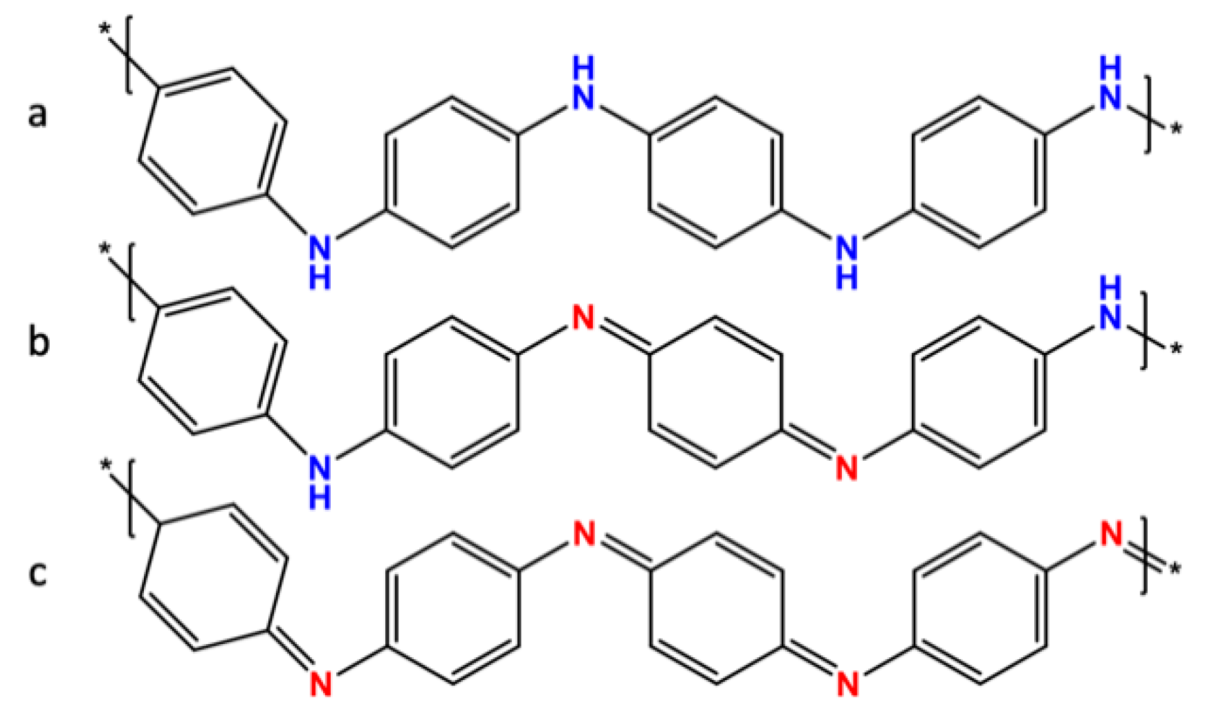
:1. Introduction
2. Materials and Methods
3. Results
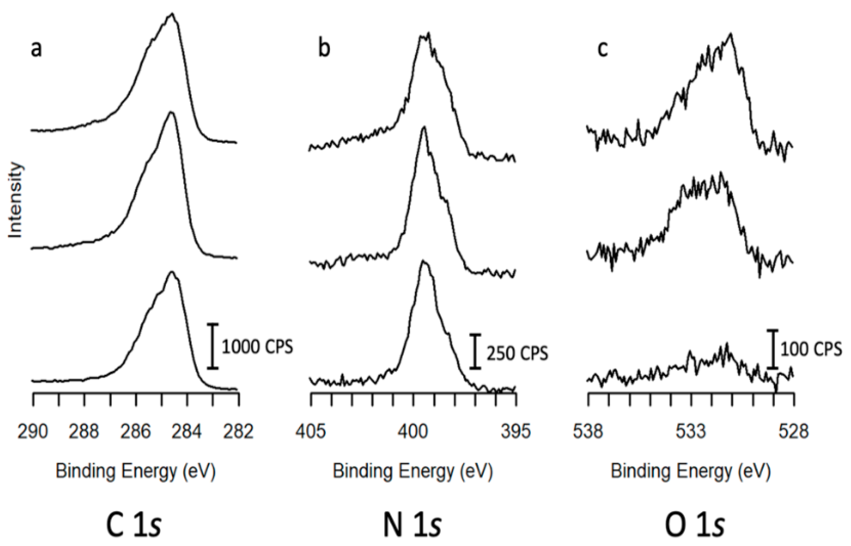
3.1. XPS
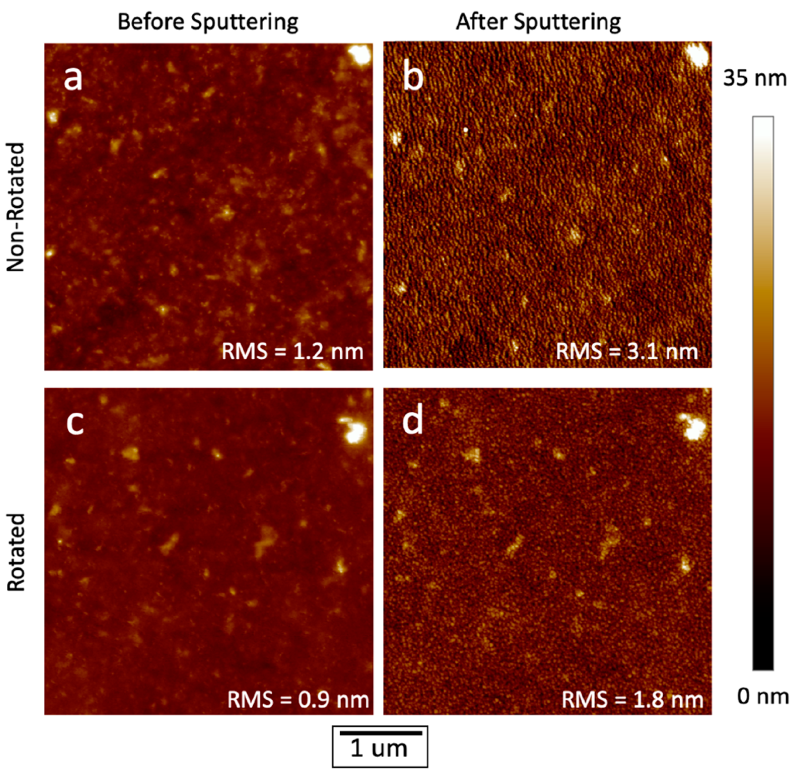
3.2. AFM
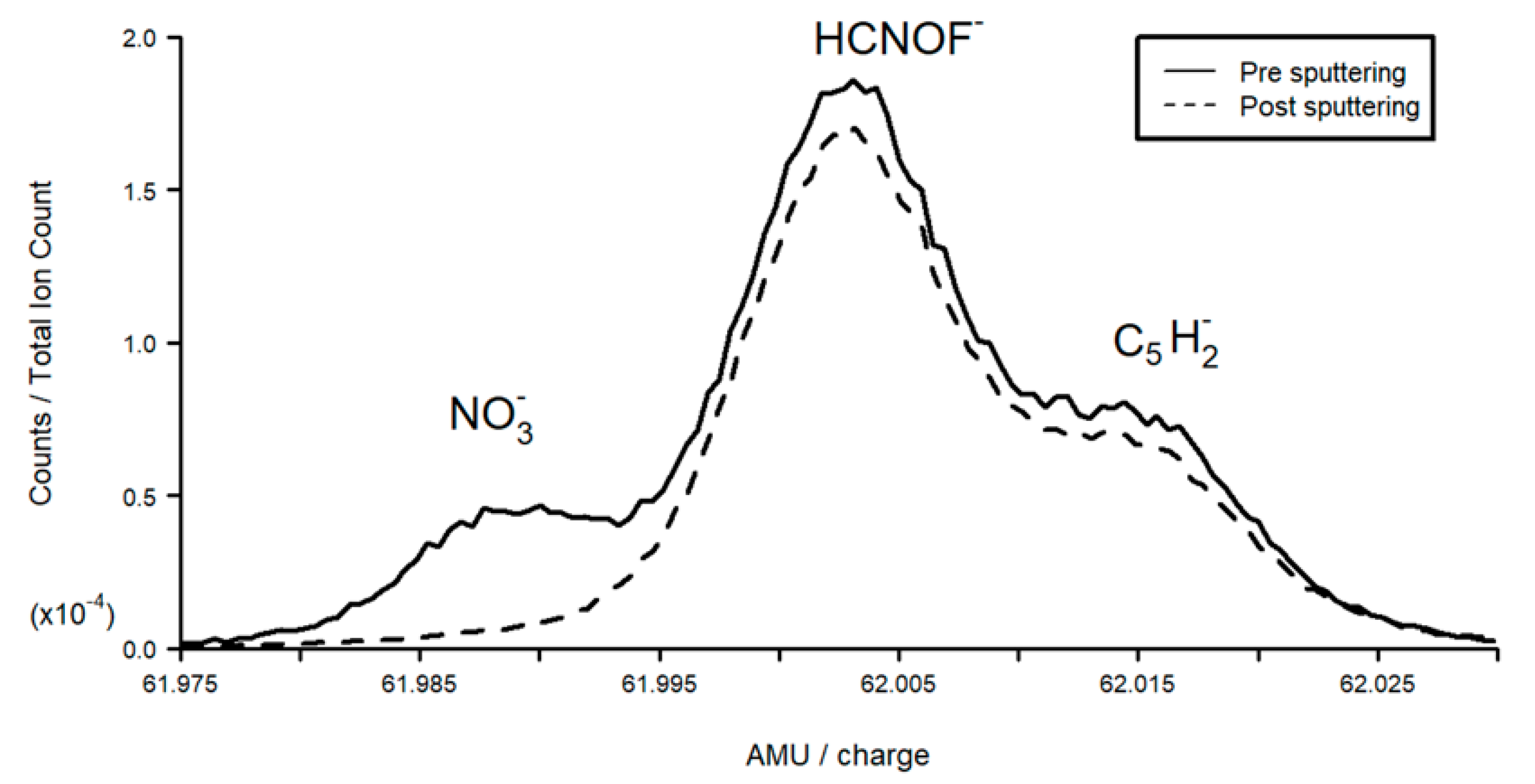
3.3. TOF-SIMS
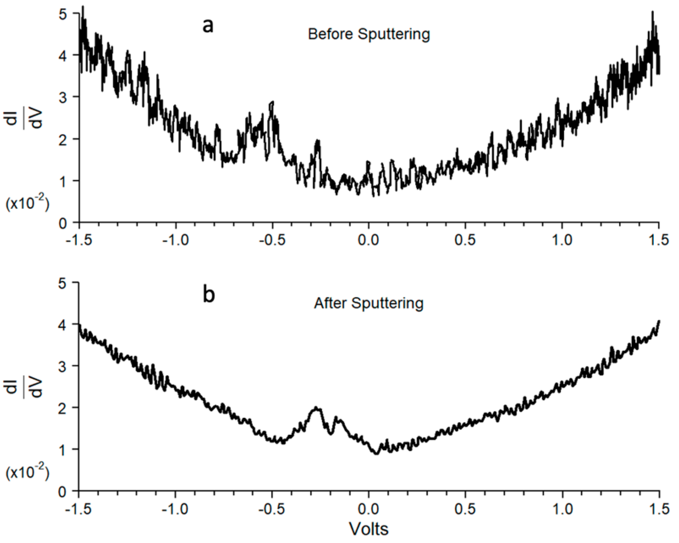
3.4. STS
4. Conclusions
Author Contributions
Funding
Conflicts of Interest
References
- MacDiarmid, A.G. “Synthetic metals”: A novel role for organic polymers (Nobel lecture). Angew. Chem. Int. 2001, 40, 2581–2590. [Google Scholar] [CrossRef]
- Soto-Oviedo, M.A.; Araújo, O.A.; Faez, R.; Rezende, M.C.; de Paoli, M.-A. Antistatic coating and electromagnetic shielding properties of a hybrid material based on polyaniline/organoclay nanocomposite and EPDM rubber. Synth. Met. 2006, 156, 1249–1255. [Google Scholar] [CrossRef]
- Bélanger, D.; Ren, X.; Davey, J.; Uribe, F.; Gottesfeld, S. Characterization and Long-Term Performance of Polyaniline-Based Electrochemical Capacitors. J. Electrochem. Soc. 2000, 147, 2923–2929. [Google Scholar] [CrossRef]
- Talo, A.; Passiniemi, P.; Forsén, O.; Yläsaari, S. Polyaniline/epoxy coatings with good anti-corrosion properties. Synth. Met. 1997, 85, 1333–1334. [Google Scholar] [CrossRef]
- Kraljić, M.; Mandić, Z.; Duić, L. Inhibition of steel corrosion by polyaniline coatings. Corros. Sci. 2003, 45, 181–198. [Google Scholar] [CrossRef]
- Menegazzo, N.; Boyne, D.; Bui, H.; Beebe, T.P., Jr.; Booksh, K.S. DC Magnetron Sputtered Polyaniline-HCl Thin Films for Chemical Sensing Applications. Anal. Chem. 2012, 84, 5770–5777. [Google Scholar] [CrossRef] [PubMed]
- Menegazzo, N.; Herbert, B.; Banerji, S.; Booksh, K.S. Discourse on the utilization of polyaniline coatings for surface plasmon resonance sensing of ammonia vapor. Talanta 2011, 85, 1369–1375. [Google Scholar] [CrossRef]
- Adhikari, S.; Banerji, P. Enhanced conductivity in iodine doped polyaniline thin film formed by thermal evaporation. Thin Solid Films 2010, 518, 5421–5425. [Google Scholar] [CrossRef]
- Cao, Y.; Treacy, G.M.; Smith, P.; Heeger, A.J. Solution-Cast Films of Polyaniline—Optical-Quality Transparent Electrodes. Appl. Phys. Lett. 1992, 60, 2711–2713. [Google Scholar] [CrossRef]
- Shimano, J.Y.; MacDiarmid, A.G. Polyaniline, a dynamic block copolymer: Key to attaining its intrinsic conductivity? Synth. Met. 2001, 123, 251–262. [Google Scholar] [CrossRef]
- Nguyen, T.D.; Camalet, J.-L.; Lacroix, J.-C.; Aeiyach, S.; Pham, M.C.; Lacaze, P.-C. Polyaniline electrodeposition from neutral aqueous media: Application to the deposition on oxidizable metals. Synth. Met. 1999, 102, 1388–1389. [Google Scholar] [CrossRef]
- Prokes, J.; Trchova, M.; Hlavata, D.; Stejskal, J. Conductivity ageing in temperature-cycled polyaniline. Polym. Degrad. Stab. 2002, 78, 393–401. [Google Scholar] [CrossRef]
- Bich, C.; Havelund, R.; Moellers, R.; Touboul, D.; Kollmer, F.; Niehuis, E.; Gilmore, I.S.; Brunelle, A. Argon Cluster Ion Source Evaluation on Lipid Standards and Rat Brain Tissue Samples. Anal. Chem. 2013, 85, 7745–7752. [Google Scholar] [CrossRef] [PubMed]
- Winograd, N. The magic of cluster SIMS. Anal. Chem. 2005, 77, 142A–149A. [Google Scholar] [CrossRef] [Green Version]
- Paruch, R.J.; Postawa, Z.; Garrison, B.J. Seduction of Finding Universality in Sputtering Yields Due to Cluster Bombardment of Solids. Acc. Chem. Res. 2015, 48, 2529–2536. [Google Scholar] [CrossRef] [PubMed]
- Delcorte, A.; Debongnie, M. Macromolecular Sample Sputtering by Large Ar and CH4 Clusters: Elucidating Chain Size and Projectile Effects with Molecular Dynamics. J. Phys. Chem. C 2015, 119, 25868. [Google Scholar] [CrossRef]
- Shard, A.G.; Ray, S.; Seah, M.P.; Yang, L. VAMAS interlaboratory study on organic depth profiling. Surf. Interface Anal. 2011, 43, 1240–1250. [Google Scholar] [CrossRef]
- Williams, D.F.; Abel, M.-L.; Grant, E.; Hrachova, J.; Watts, J.F. Flame treatment of polypropylene: A study by electron and ion spectroscopies. Int. J. Adhes. Adhes. 2015, 63, 26–33. [Google Scholar] [CrossRef] [Green Version]
- Bernasik, A.; Haberko, J.; Marzec, M.M.; Rysz, J.; Łużny, W.; Budkowski, A. Chemical stability of polymers under argon gas cluster ion beam and x-ray irradiation. J. Vac. Sci. Technol. B 2016, 34, 30604. [Google Scholar] [CrossRef]
- Seah, M.P.; Havelund, R.; Shard, A.G.; Gilmore, I.S. Sputtering Yields for Mixtures of Organic Materials Using Argon Gas Cluster Ions. J. Phys. Chem. B 2015, 119, 13433. [Google Scholar] [CrossRef]
- Seah, M.P. Universal Equation for Argon Gas Cluster Sputtering Yields. J. Phys. Chem. C 2013, 117, 12622–12632. [Google Scholar] [CrossRef]
- Seah, M.P.; Spencer, S.J.; Shard, A.G. Angle Dependence of Argon Gas Cluster Sputtering Yields for Organic Materials. J. Phys. Chem. B 2015, 119, 3297–3303. [Google Scholar] [CrossRef] [PubMed]
- Shard, A.G.; Havelund, R.; Spencer, S.J.; Gilmore, I.S.; Alexander, M.R.; Angerer, T.B.; Aoyagi, S.; Barnes, J.-P.; Benayad, A.; Bernasik, A.; et al. Measuring Compositions in Organic Depth Profiling: Results from a VAMAS Interlaboratory Study. J. Phys. Chem. B 2015, 119, 10784. [Google Scholar] [CrossRef]
- Shard, A.G.; Havelund, R.; Seah, M.P.; Spencer, S.J.; Gilmore, I.S.; Winograd, N.; Mao, D.; Miyayama, T.; Niehuis, E.; Rading, D.; et al. Argon Cluster Ion Beams for Organic Depth Profiling: Results from a VAMAS Interlaboratory Study. Anal. Chem. 2012, 84, 7865–7873. [Google Scholar] [CrossRef]
- Taylor, A.J.; Graham, D.J.; Castner, D.G. Reconstructing accurate ToF-SIMS depth profiles for organic materials with differential sputter rates. Analyst 2015, 140, 6005–6014. [Google Scholar] [CrossRef] [Green Version]
- Chu, Y.-H.; Liao, H.-Y.; Lin, K.-Y.; Chang, H.-Y.; Kao, W.-L.; Kuo, D.-Y.; You, Y.-W.; Chu, K.-J.; Wu, C.-Y.; Shyue, J.-J. Improvement of Gas Cluster Ion Beam- (GCIB)-Based Molecular Secondary Ion Mass Spectroscopy (SIMS) Depth Profile with O2+ Cosputtering. Analyst 2016, 141, 2523. [Google Scholar] [CrossRef]
- You, Y.-W.; Chang, H.-Y.; Lin, W.-C.; Kuo, C.-H.; Lee, S.-H.; Kao, W.-L.; Yen, G.-J.; Chang, C.-J.; Liu, C.-P.; Huang, C.-C.; et al. Molecular dynamic-secondary ion mass spectrometry (D-SIMS) ionized by co-sputtering with C60+ and Ar+. Rapid Commun. Mass Spectrom. 2011, 25, 2897–2904. [Google Scholar] [CrossRef] [PubMed]
- Goodwin, C.M.; Voras, Z.E.; Beebe, T.P. Gas-cluster ion sputtering: Effect on organic layer morphology. J. Vac. Sci. Technol. A 2018, 36, 051507. [Google Scholar] [CrossRef]
- Strawhecker, K.E.; Kumar, S.K.; Douglas, J.F.; Karim, A. The critical role of solvent evaporation on the roughness of spin-cast polymer films. Macromolecules 2001, 34, 4669–4672. [Google Scholar] [CrossRef]
- Sehgal, T.; Rattan, S. Synthesis, characterization and swelling characteristics of graft copolymerized isotactic polypropylene film. Int. J. Polym. Sci. 2010, 2010. [Google Scholar] [CrossRef]
- Doroudiani, S.; Park, C.B.; Kortschot, M.T. Effect of the crystallinity and morphology on the microcellular foam structure of semicrystalline polymers. Polym. Eng. Sci. 1996, 36, 2645–2662. [Google Scholar] [CrossRef]
- Bhattacharya, A.; Misra, B.N. Grafting: A versatile means to modify polymers—Techniques, factors and applications. Prog. Polym. Sci. 2004, 29, 767–814. [Google Scholar] [CrossRef]
- Yoshida, W.; Cohen, Y. Topological AFM characterization of graft polymerized silica membranes. J. Membr. Sci. 2003, 215, 249–264. [Google Scholar] [CrossRef]
- Coburn, J.W. Surface Processing with Partially Ionized Plasmas. IEEE Trans. Plasma Sci. 1991, 19, 1048–1062. [Google Scholar] [CrossRef]
- Lanauze, J.A.; Myers, D.L. Ink Adhesion on Corona-Treated Polyethylene Studied by Chemical Derivatization of Surface Functional Groups. J. Appl. Polym. Sci. 1990, 40, 595–611. [Google Scholar] [CrossRef]
- Abdulrazzaq, O.; Bourdo, S.E.; Saini, V.; Bairi, V.G.; Dervishi, E.; Viswanathan, T.; Nima, Z.A.; Biris, A.S. Optimization of the Protonation Level of Polyaniline-Based Hole-Transport Layers in Bulk-Heterojunction Organic Solar Cells. Energy Technol. 2013, 1, 463–470. [Google Scholar] [CrossRef]
- Ton-That, C.; Shard, A.G.; Bradley, R.H. Thickness of spin-cast polymer thin films determined by angle-resolved XPS and AFM tip-scratch methods. Langmuir 2000, 16, 2281–2284. [Google Scholar] [CrossRef]
- Sreedhar, B.; Sairam, M.; Chattopadhyay, D.K.; Mitra, P.P.; Rao, D.V.M. Thermal and XPS studies on polyaniline salts prepared by inverted emulsion polymerization. J. Appl. Polym. Sci. 2006, 101, 499–508. [Google Scholar] [CrossRef]
- Furukawa, Y.; Ueda, F.; Hyodo, Y.; Harada, I.; Nakajima, T.; Kawagoe, T. Vibrational-Spectra and Structure of Polyaniline. Macromolecules 1988, 21, 1297–1305. [Google Scholar] [CrossRef]
- Zalar, A. Improved Depth Resolution by Sample Rotation during Auger-Electron Spectroscopy Depth Profiling. Thin Solid Films 1985, 124, 223–230. [Google Scholar] [CrossRef]
- Chan, H.S.O.; Ang, S.G.; Ho, P.K.H.; Johnson, D. Static Secondary Ion Mass-Spectrometry (Sims) of Polyanilines—A Preliminary-Study. Synth. Met. 1990, 36, 103–110. [Google Scholar] [CrossRef]
- Narayanan, T.N.; Jose, S.; Thomas, S.; Al-Harthi, S.H.; Anantharaman, M.R. Fabrication of a quantum well heterostructure based on plasma polymerized aniline and its characterization using STM/STS. J. Phys. D Appl. Phys. 2009, 42, 165309. [Google Scholar] [CrossRef]
- Hassanien, A.; Gao, M.; Tokumoto, M.; Dai, L. Scanning tunneling microscopy of aligned coaxial nanowires of polyaniline passivated carbon nanotubes. Chem. Phys. Lett. 2001, 342, 479–484. [Google Scholar] [CrossRef]


| Sample | Carbon | Nitrogen | Oxygen |
|---|---|---|---|
| Powder | 85.2 ± 0.4% | 11.7 ± 0.5% | 3.2 ± 0.4% |
| Film | 84.9 ± 0.3% | 12.2 ± 0.3% | 2.9 ± 0.5% |
| Post sputter | 86.7 ± 0.2% | 12.6 ± 0.2% | 0.8 ± 0.6% |
| Bulk values 1 | 86% | 14% | - |
© 2020 by the authors. Licensee MDPI, Basel, Switzerland. This article is an open access article distributed under the terms and conditions of the Creative Commons Attribution (CC BY) license (http://creativecommons.org/licenses/by/4.0/).
Share and Cite
Goodwin, C.M.; Voras, Z.E.; Tong, X.; Beebe, T.P., Jr. Soft Ion Sputtering of PAni Studied by XPS, AFM, TOF-SIMS, and STS. Coatings 2020, 10, 967. https://doi.org/10.3390/coatings10100967
Goodwin CM, Voras ZE, Tong X, Beebe TP Jr. Soft Ion Sputtering of PAni Studied by XPS, AFM, TOF-SIMS, and STS. Coatings. 2020; 10(10):967. https://doi.org/10.3390/coatings10100967
Chicago/Turabian StyleGoodwin, Christopher M., Zachary E. Voras, Xiao Tong, and Thomas P. Beebe, Jr. 2020. "Soft Ion Sputtering of PAni Studied by XPS, AFM, TOF-SIMS, and STS" Coatings 10, no. 10: 967. https://doi.org/10.3390/coatings10100967