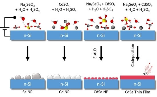
Electrodeposition of Nanoparticles and Continuous Film of CdSe on n-Si (100)

 ,
,  , , ,
, , , 
 , ,
, ,
Abstract
:
1. Introduction
2. Materials and Methods
2.1. Electrochemical Measurements
2.2. Microscopic and Spectroscopic Characterization
3. Results
3.1. Cadmium
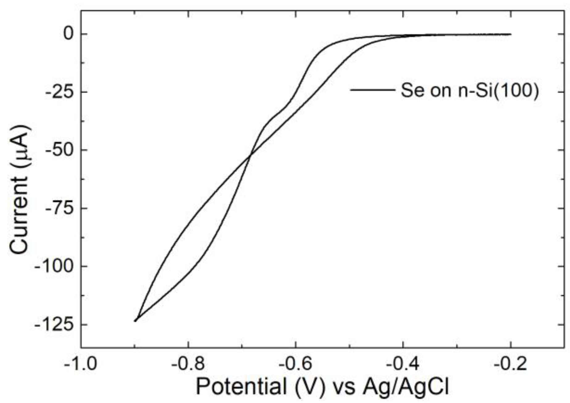
3.2. Selenium
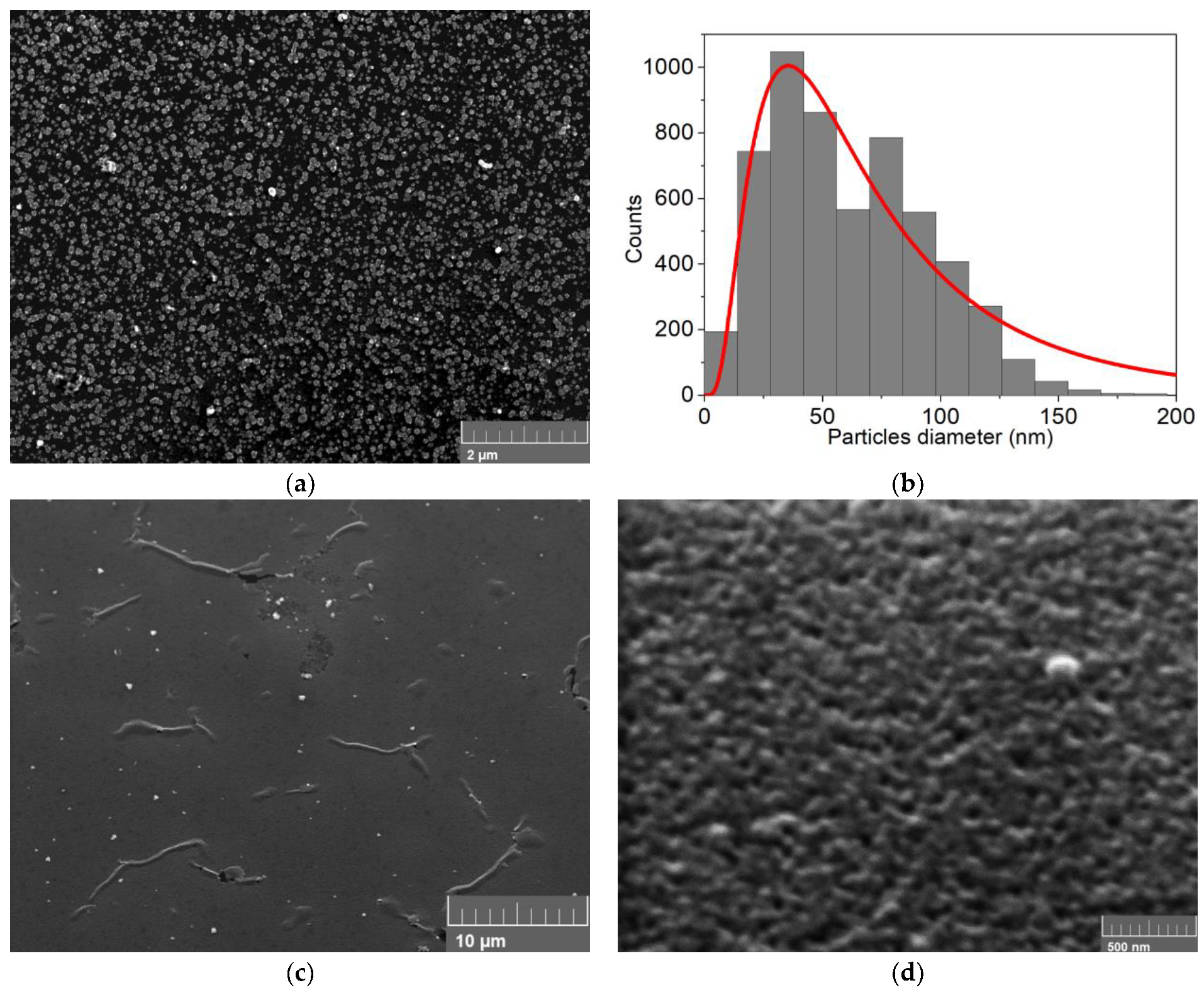
3.3. Cadmium Selenide
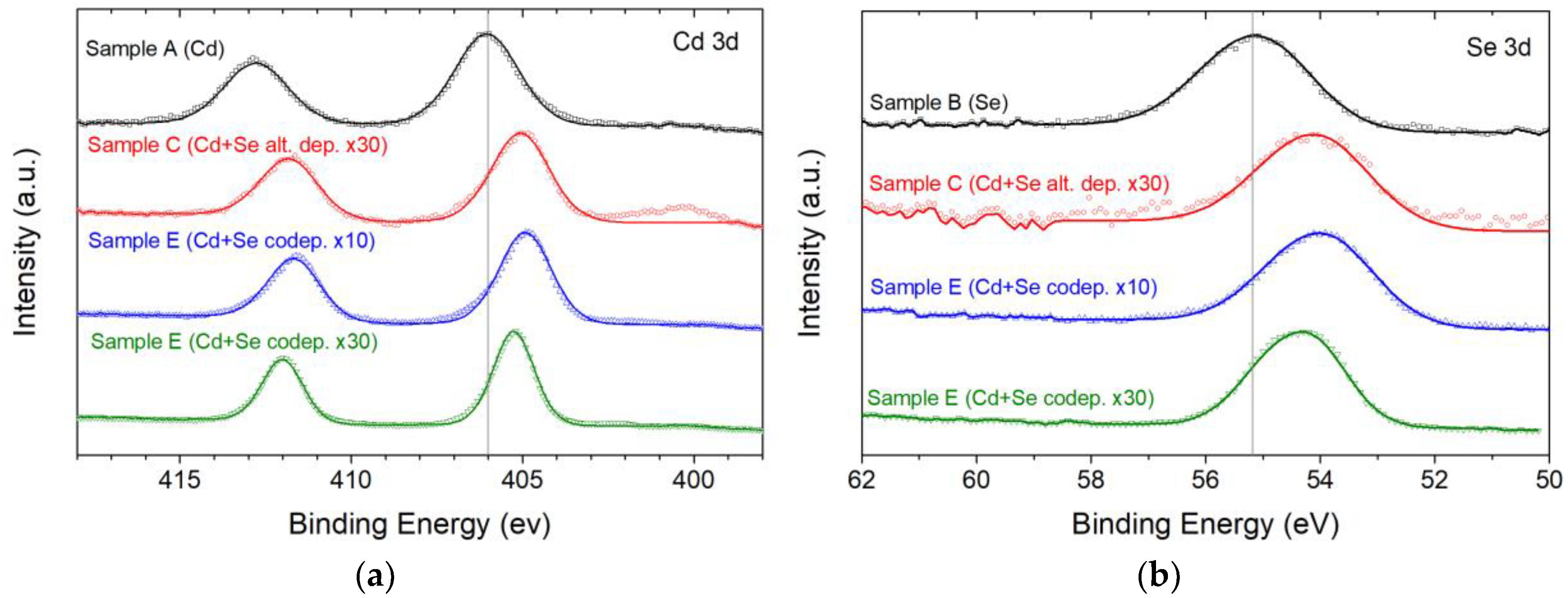
3.4. Spectroscopic Characterizations
4. Conclusions
Supplementary Materials
Author Contributions
Funding
Acknowledgments
Conflicts of Interest
References
- Kalem, S.; Werner, P.; Talalaev, V. Near-IR photoluminescence from Si/Ge nanowire-grown silicon wafers: Effect of HF treatment. Appl. Phys. A Mater. Sci. Process. 2013, 112, 561–567. [Google Scholar] [CrossRef]
- Iacona, F.; Pacifici, D.; Irrera, A.; Miritello, M.; Franzò, G.; Priolo, F.; Sanfilippo, D.; Di Stefano, G.; Fallica, P.G. Electroluminescence at 1.54 μm in Er-doped Si nanocluster-based devices. Appl. Phys. Lett. 2002, 81, 3242–3244. [Google Scholar] [CrossRef]
- Irrera, A.; Lo Faro, M.J.; D’Andrea, C.; Alessio Leonardi, A.; Artoni, P.; Fazio, B.; Anna Picca, R.; Cioffi, N.; Trusso, S.; Franzo, G.; et al. Light-emitting silicon nanowires obtained by metal-assisted chemical etching. Semicond. Sci. Technol. 2017, 32. [Google Scholar] [CrossRef]
- Credo, G.M.; Mason, M.D.; Buratto, S.K. External quantum efficiency of single porous silicon nanoparticles. Appl. Phys. Lett. 1999, 74, 1978–1980. [Google Scholar] [CrossRef]
- Chiappini, C.; Liu, X.; Fakhoury, J.R.; Ferrari, M. Biodegradable porous silicon barcode nanowires with defined geometry. Adv. Funct. Mater. 2010, 20, 2231–2239. [Google Scholar] [CrossRef]
- Erogbogbo, F.; Yong, K.T.; Hu, R.; Law, W.C.; Ding, H.; Chang, C.W.; Prasad, P.N.; Swihart, M.T. Biocompatible magnetofluorescent probes: Luminescent silicon quantum dots coupled with superparamagnetic iron (III) oxide. ACS Nano 2010, 4, 5131–5138. [Google Scholar] [CrossRef]
- Donato, M.G.; Brzobohatý, O.; Simpson, S.H.; Irrera, A.; Leonardi, A.A.; Lo Faro, M.J.; Svak, V.; Maragò, O.M.; Zemánek, P. Optical Trapping, Optical Binding, and Rotational Dynamics of Silicon Nanowires in Counter-Propagating Beams. Nano Lett. 2019, 19, 342–352. [Google Scholar] [CrossRef]
- Li, H.; Ye, T.; Shi, L.; Xie, C. Fabrication of ultra-high aspect ratio (>160:1) silicon nanostructures by using Au metal assisted chemical etching. J. Micromech. Microeng. 2017, 27. [Google Scholar] [CrossRef]
- Leonardi, A.A.; Lo Faro, M.J.; Petralia, S.; Fazio, B.; Musumeci, P.; Conoci, S.; Irrera, A.; Priolo, F. Ultrasensitive Label- and PCR-Free Genome Detection Based on Cooperative Hybridization of Silicon Nanowires Optical Biosensors. ACS Sens. 2018, 3, 1690–1697. [Google Scholar] [CrossRef]
- Irrera, A.; Leonardi, A.A.; Di Franco, C.; Lo Faro, M.J.; Palazzo, G.; D’Andrea, C.; Manoli, K.; Franzò, G.; Musumeci, P.; Fazio, B.; et al. New Generation of Ultrasensitive Label-Free Optical Si Nanowire-Based Biosensors. ACS Photonics 2018, 5, 471–479. [Google Scholar] [CrossRef]
- Cui, Y.; Wei, Q.; Park, H.; Lieber, C.M. Nanowire Nanosensors for Highly Sensitive and Selective Detection of Biological and Chemical Species. Science 2001, 293, 1289–1292. [Google Scholar] [CrossRef] [PubMed]
- Patolsky, F.; Zheng, G.; Lieber, C.M. Nanowire sensors for medicine and the life sciences. Nanomedicine 2006, 1, 51–65. [Google Scholar] [CrossRef] [PubMed] [Green Version]
- Garnett, E.; Yang, P. Light trapping in silicon nanowire solar cells. Nano Lett. 2010, 10, 1082–1087. [Google Scholar] [CrossRef] [PubMed]
- Tian, B.; Zheng, X.; Kempa, T.J.; Fang, Y.; Yu, N.; Yu, G.; Huang, J.; Lieber, C.M. Coaxial silicon nanowires as solar cells and nanoelectronic power sources. Energy 2007, 449, 885–889. [Google Scholar] [CrossRef]
- Pecora, E.F.; Lawrence, N.; Gregg, P.; Trevino, J.; Artoni, P.; Irrera, A.; Priolo, F.; Negro, L.D. Nanopatterning of silicon nanowires for enhancing visible photoluminescence. Nanoscale 2012, 4, 2863–2866. [Google Scholar] [CrossRef] [PubMed]
- Fazio, B.; Irrera, A.; Pirotta, S.; D’Andrea, C.; Del Sorbo, S.; Josè Lo Faro, M.; Gucciardi, P.G.; Iatì, M.A.; Saija, R.; Patrini, M.; et al. Coherent backscattering of Raman light. Nat. Photonics 2017, 11, 170–176. [Google Scholar] [CrossRef]
- Walavalkar, S.S.; Hofmann, C.E.; Homyk, A.P.; Henry, M.D.; Atwater, H.A.; Scherer, A. Tunable visible and near-IR emission from sub-10 nm etched single-crystal Si nanopillars. Nano Lett. 2010, 10, 4423–4428. [Google Scholar] [CrossRef] [PubMed]
- José Lo Faro, M.; Alessio Leonardi, A.; Morganti, D.; Fazio, B.; Vasi, C.; Musumeci, P.; Priolo, F.; Irrera, A. Low cost fabrication of Si NWs/cui heterostructures. Nanomaterials 2018, 8, 569. [Google Scholar] [CrossRef]
- Qiao, L.; Li, D.; Postolova, S.V.; Mironov, A.Y.; Vinokur, V.; Rosenstein, B. Dynamical instability of the electric transport in superconductors. Sci. Rep. 2018, 8, 14104. [Google Scholar] [CrossRef]
- Tarabrin, M.K.; Ustinov, D.V.; Tomilov, S.M.; Lazarev, V.A.; Karasik, V.E.; Kozlovsky, V.I.; Korostelin, Y.V.; Skasyrsky, Y.K.; Frolov, M.P. Highly efficient continuous wave single mode Cr:CdSe laser with output power more than 2 W. In Laser Congress 2018 (ASSL); OSA Technical Digest; Optical Society of America: Boston, MS, USA, 2018; p. AW3A.8. [Google Scholar]
- Zhao, J.; Bardecker, J.A.; Munro, A.M.; Liu, M.S.; Niu, Y.; Ding, I.K.; Luo, J.; Chen, B.; Jen, A.K.Y.; Ginger, D.S. Efficient CdSe/CdS quantum dot light-emitting diodes using a thermally polymerized hole transport layer. Nano Lett. 2006, 6, 463–467. [Google Scholar] [CrossRef]
- Shaikh, A.V.; Mane, R.S.; Joo, O.S.; Han, S.H.; Pathan, H.M. Electrochemical deposition of cadmium selenide films and their properties: A review. J. Solid State Electrochem. 2017, 21, 2517–2530. [Google Scholar] [CrossRef]
- Kowalik, R.; Kazimierczak, H.; Zabiński, P. Electrodeposition of cadmium selenide. Mater. Sci. Semicond. Process. 2016, 50, 43–48. [Google Scholar] [CrossRef]
- Kowalik, R. Electrodeposition of CdSe by ECALD from Citric Buffer. J. Electrochem. Soc. 2016, 163, D282–D286. [Google Scholar] [CrossRef]
- Chong, B.; Zhu, W.; Liu, Y.; Guan, L.; Chen, G.Z. Highly efficient photoanodes based on cascade structural semiconductors of Cu2Se/CdSe/TiO2: A multifaceted approach to achieving microstructural and compositional control. J. Mater. Chem. A 2016, 4, 1336–1344. [Google Scholar] [CrossRef]
- Feng, S.; Wu, J.; Hu, P.; Chen, Y.; Ma, B.; Peng, J.; Yang, J.; Jiang, H. Epitaxial growth of successive CdSe ultrathin films and quantum dot layers on TiO 2 nanorod arrays for photo-electrochemical cells. RSC Adv. 2014, 4, 12154–12159. [Google Scholar] [CrossRef]
- Cabral, M.F.; Coelho, D.; MacHado, S.A.S. Analyzing Cd underpotential deposition behavior on Se thin-films: Atomic force microscopy, cyclic voltammetry and electrochemical quartz crystal nanobalance studies. Electrochim. Acta 2013, 91, 361–366. [Google Scholar] [CrossRef]
- Bieńkowski, K.; Strawski, M.; Maranowski, B.; Szklarczyk, M. Studies of stoichiometry of electrochemically grown CdSe deposits. Electrochim. Acta 2010, 55, 8908–8915. [Google Scholar] [CrossRef]
- Loglio, F.; Innocenti, M.; D’Acapito, F.; Felici, R.; Pezzatini, G.; Salvietti, E.; Foresti, M.L. Cadmium selenide electrodeposited by ECALE: Electrochemical characterization and preliminary results by EXAFS. J. Electroanal. Chem. 2005, 575, 161–167. [Google Scholar] [CrossRef]
- Cecconi, T.; Atrei, A.; Bardi, U.; Forni, F.; Innocenti, M.; Loglio, F.; Foresti, M.L.; Rovida, G. X-ray photoelectron diffraction (XPD) study of the atomic structure of the ultrathin CdS phase deposited on Ag (111) by electrochemical atomic layer epitaxy (ECALE). J. Electron Spectrosc. Relat. Phenom. 2001, 114–116, 563–568. [Google Scholar] [CrossRef]
- Chubenko, E.B.; Klyshko, A.A.; Petrovich, V.A.; Bondarenko, V.P. Electrochemical deposition of zinc selenide and cadmium selenide onto porous silicon from aqueous acidic solutions. Thin Solid Films 2009, 517, 5981–5987. [Google Scholar] [CrossRef]
- Forni, F.; Innocenti, M.; Pezzatini, G.; Foresti, M.L. Electrochemical aspects of CdTe growth on the face (111) of silver by ECALE. Electrochim. Acta 2000, 45, 3225–3231. [Google Scholar] [CrossRef]
- Shirley, D.A. High-resolution x-ray photoemission spectrum of the valence bands of gold. Phys. Rev. B 1972, 5, 4709–4714. [Google Scholar] [CrossRef]
- Susi, T.; Pichler, T.; Ayala, P. X-ray photoelectron spectroscopy of graphitic carbon nanomaterials doped with heteroatoms. Beilstein J. Nanotechnol. 2015, 6, 177–192. [Google Scholar] [CrossRef] [PubMed] [Green Version]
- Kerby, R.C.; Jackson, H.E.; O’Keefe, T.J.; Wang, Y.M. Evaluation of organic additives for use in zinc electrowinning. Metall. Trans. B 1977, 8, 661–668. [Google Scholar] [CrossRef]
- Mackinnon, D.J.; Brannen, J.M. Zinc deposit structures obtained from high purity synthetic and industrial acid sulphate electrolytes with and without antimony and glue additions. J. Appl. Electrochem. 1977, 7, 451–459. [Google Scholar] [CrossRef]
- Adcock, P.A.; Quillinan, A.; Clark, B.; Newman, O.M.G.; Adeloju, S.B. Measurement of polarization parameters impacting on electrodeposit morphology. II: Conventional zinc electrowinning solutions. J. Appl. Electrochem. 2004, 34, 771–780. [Google Scholar] [CrossRef]
- Isa, N.N.C.; Mohd, Y. Cyclic voltammetric study of stainless steel substrate in acidic Cuso4 solution. Solid State Sci. Technol. 2017, 25, 103–110. [Google Scholar]
- Tumelero, M.A.; Benetti, L.C.; Isoppo, E.; Faccio, R.; Zangari, G.; Pasa, A.A. Electrodeposition and ab Initio Studies of Metastable Orthorhombic Bi2Se3: A Novel Semiconductor with Bandgap for Photovoltaic Applications. J. Phys. Chem. C 2016, 120, 11797–11806. [Google Scholar] [CrossRef]
- Singh, A.; Chowdhury, D.R.; Paul, A. A kinetic study of ferrocenium cation decomposition utilizing an integrated electrochemical methodology composed of cyclic voltammetry and amperometry. Analyst 2014, 139, 5747–5754. [Google Scholar] [CrossRef]
- Bard, A.J.; Faulkner, L.R. Electrochemical Methods Fundamentals and Applications; John Wiley & Sons Inc.: Hoboken, NJ, USA, 2000; ISBN 0-471-04372-9. [Google Scholar]
- Jones, D.A.; Walker, R. Principles and Prevention of Corrosion: Pearson New International Edition; Pearson Higher Ed USA: New York, NY, USA, 1995; ISBN 0-13-359993-0. [Google Scholar]
- Michaelson, H.B. The work function of the elements and its periodicity. J. Appl. Phys. 1977, 48, 4729–4733. [Google Scholar] [CrossRef] [Green Version]
- Velusamy, P.; Babu, R.R.; Ramamurthi, K.; Elangovan, E.; Viegas, J.; Dahlem, M.S.; Arivanandhan, M. Characterization of spray pyrolytically deposited high mobility praseodymium doped CdO thin films. Ceram. Int. 2016, 42, 12675–12685. [Google Scholar] [CrossRef]
- Tkachenko, O.P.; Shpiro, E.S.; Wark, M.; Schulz-Ekloff, G.; Jaeger, N.I. X-ray photoelectron/X-ray excited auger electron spectroscopic study of highly dispersed semiconductor CdS and CdO species in zeolites. J. Chem. Soc. Faraday Trans. 1993, 89, 3987–3994. [Google Scholar] [CrossRef]
- Agostinelli, E.; Battistoni, C.; Fiorani, D.; Mattogno, G.; Nogues, M. An XPS study of the electronic structure of the ZnxCd1-xCr2(X = S, Se) spinel system. J. Phys. Chem. Solids 1989, 50, 269–272. [Google Scholar] [CrossRef]
- Cahen, D.; Ireland, P.J.; Kazmerski, L.L.; Thiel, F.A. X-ray photoelectron and Auger electron spectroscopic analysis of surface treatments and electrochemical decomposition of CuInSe2 photoelectrodes. J. Appl. Phys. 1985, 57, 4761–4771. [Google Scholar] [CrossRef]
- Chen, M.L.; Oh, W.C. Synthesis and highly visible-induced photocatalytic activity of CNT-CdSe composite for methylene blue solution. Nanoscale Res. Lett. 2011, 6, 398. [Google Scholar] [CrossRef]
- Sapra, S.; Rogach, A.L.; Feldmann, J. Phosphine-free synthesis of monodisperse CdSe nanocrystals in olive oil. J. Mater. Chem. 2006, 16, 3391–3395. [Google Scholar] [CrossRef]
- Semaltianos, N.G.; Logothetidis, S.; Perrie, W.; Romani, S.; Potter, R.J.; Sharp, M.; French, P.; Dearden, G.; Watkins, K.G. CdSe nanoparticles synthesized by laser ablation. EPL 2008, 84. [Google Scholar] [CrossRef]


| Sample | Description |
|---|---|
| A | Cd NPs, 30 nmol deposition |
| B | Se NPs, 30 nmol with deposition |
| C | CdSe NPs, 30 nmol with alternate deposition |
| D | CdSe NPs, 10 nmol with co-deposition |
| E | CdSe thin film, 30 nmol with co-deposition |
© 2019 by the authors. Licensee MDPI, Basel, Switzerland. This article is an open access article distributed under the terms and conditions of the Creative Commons Attribution (CC BY) license (http://creativecommons.org/licenses/by/4.0/).
Share and Cite
Giurlani, W.; Dell’Aquila, V.; Vizza, M.; Calisi, N.; Lavacchi, A.; Irrera, A.; Lo Faro, M.J.; Leonardi, A.A.; Morganti, D.; Innocenti, M. Electrodeposition of Nanoparticles and Continuous Film of CdSe on n-Si (100). Nanomaterials 2019, 9, 1504. https://doi.org/10.3390/nano9101504
Giurlani W, Dell’Aquila V, Vizza M, Calisi N, Lavacchi A, Irrera A, Lo Faro MJ, Leonardi AA, Morganti D, Innocenti M. Electrodeposition of Nanoparticles and Continuous Film of CdSe on n-Si (100). Nanomaterials. 2019; 9(10):1504. https://doi.org/10.3390/nano9101504
Chicago/Turabian StyleGiurlani, Walter, Vincenzo Dell’Aquila, Martina Vizza, Nicola Calisi, Alessandro Lavacchi, Alessia Irrera, Maria Josè Lo Faro, Antonio Alessio Leonardi, Dario Morganti, and Massimo Innocenti. 2019. "Electrodeposition of Nanoparticles and Continuous Film of CdSe on n-Si (100)" Nanomaterials 9, no. 10: 1504. https://doi.org/10.3390/nano9101504