Enhanced Radiation Tolerance of Tungsten Nanoparticles to He Ion Irradiation

 ,
,
Abstract
:
1. Introduction
2. Methodology
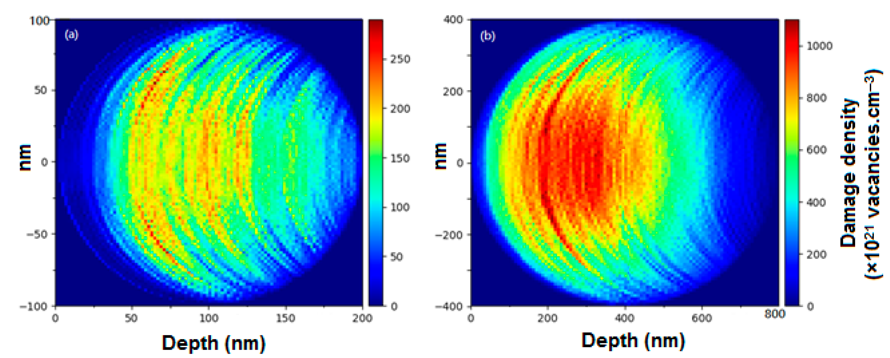
2.1. Experimental
2.2. Analysis
3. Results and Discussion
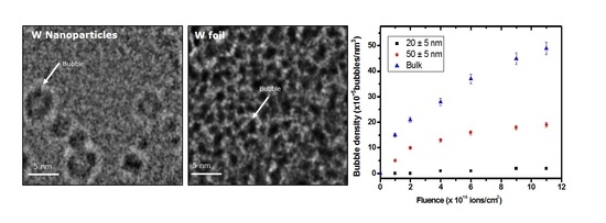
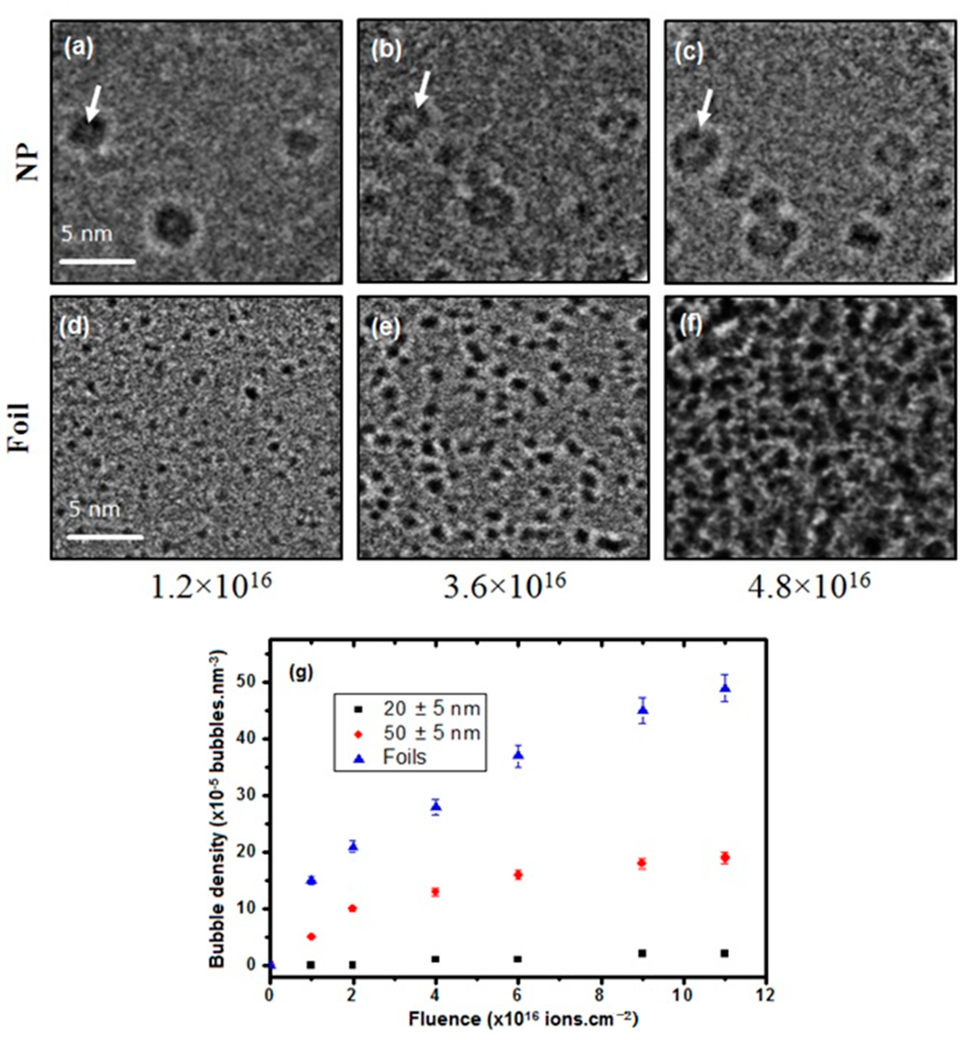
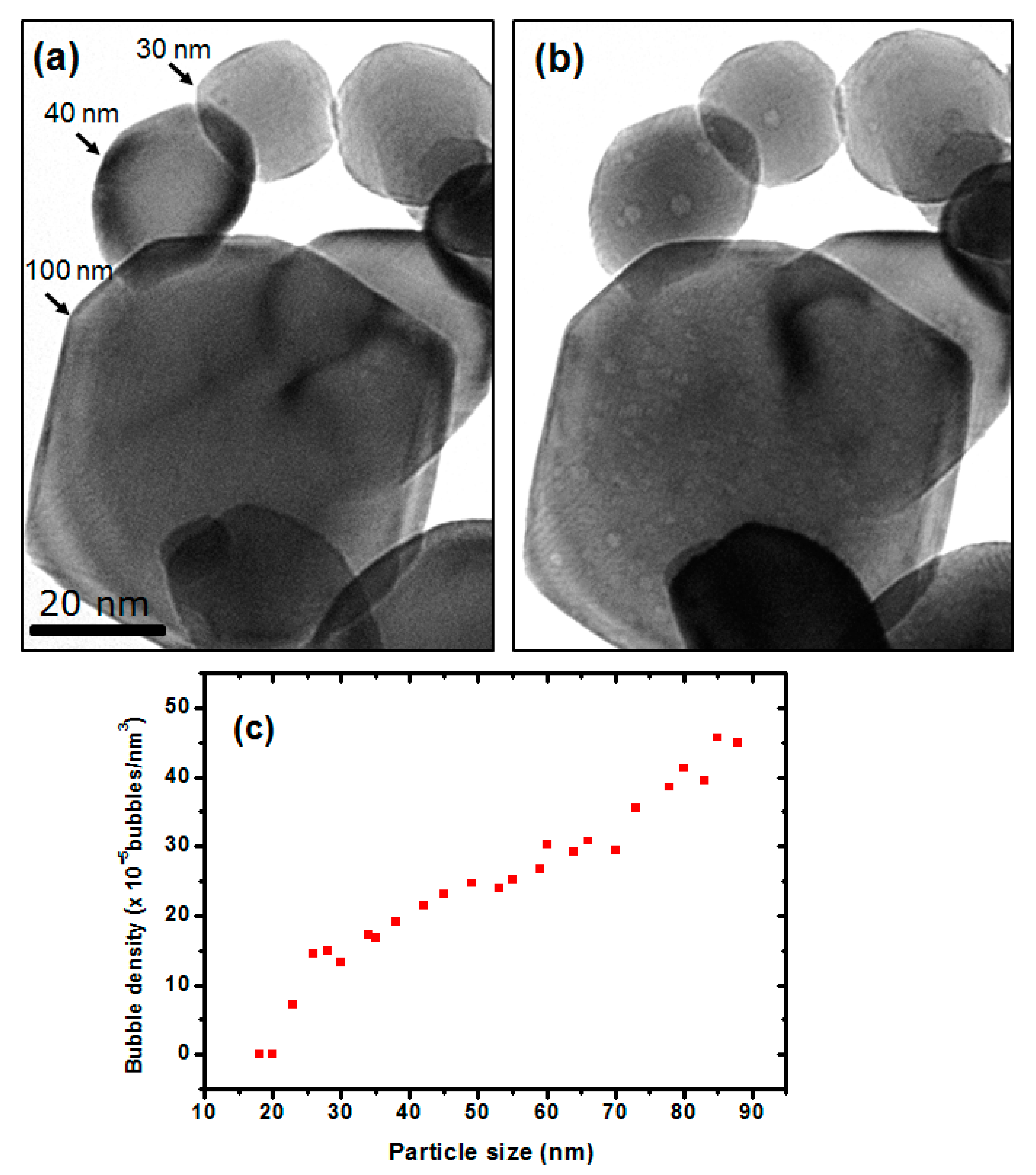
3.1. Bubble Density
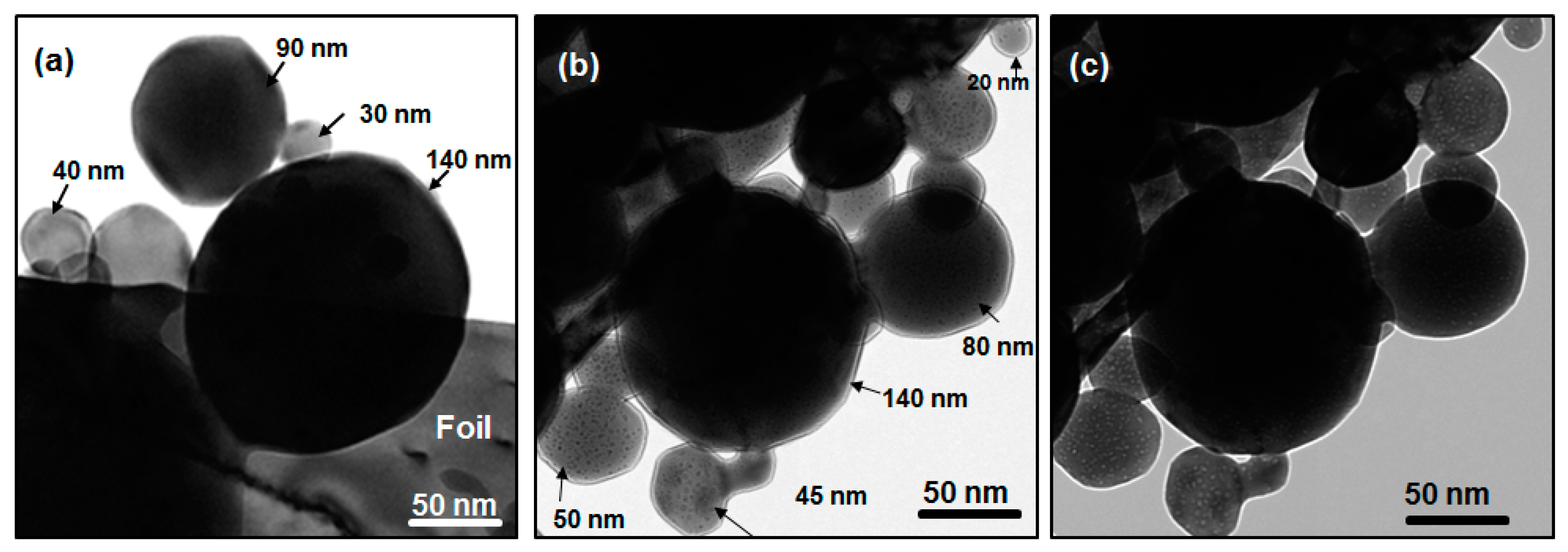
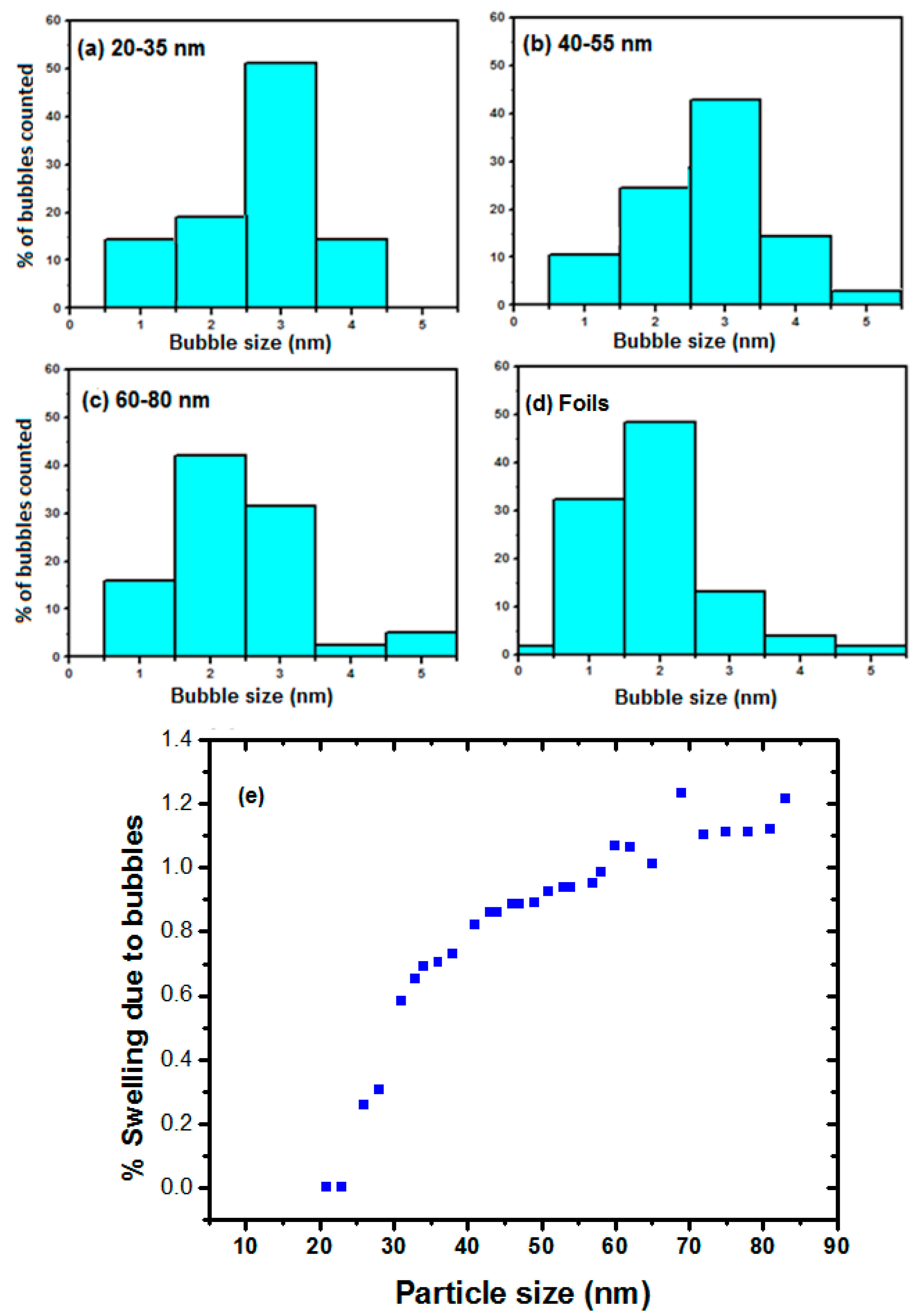
3.2. Bubble Size and Swelling Due to Bubbles
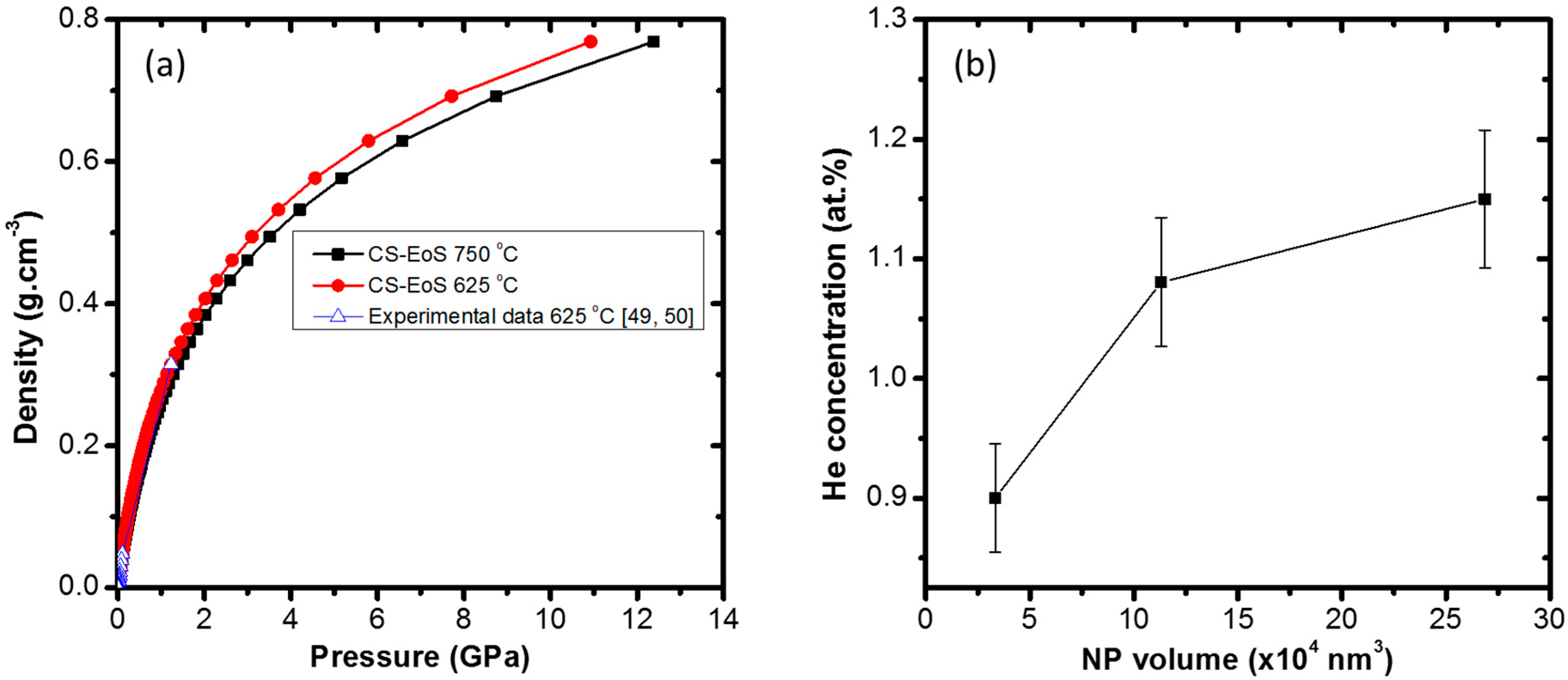
3.3. Helium Concentration in NPs
3.4. Dislocation Loops
4. Conclusions
Author Contributions
Funding
Acknowledgments
Conflicts of Interest
References
- Ongena, J.; Koch, R.; Wolf, R.; Zohm, H. Magnetic-confinement fusion. Nat. Phys. 2016, 12, 398–410. [Google Scholar] [CrossRef]
- Shimada, M.; Campbell, D.J.; Mukhovatov, V.; Fujiwara, M.; Kirneva, N.; Lackner, K.; Nagami, M.; Pustovitov, V.D.; Uckan, N.; Wesley, J.; et al. Progress in the ITER physics basis chapter 1: Overview and summary. Nucl. Fusion 2007, 47. [Google Scholar] [CrossRef]
- Tokunaga, K.; Baldwin, M.J.; Doerner, R.P.; Noda, N.; Kubota, Y.; Yoshida, N.; Sogabe, T.; Kato, T.; Schedler, B. Blister formation and deuterium retention on tungsten exposed to low energy and high flux deuterium plasma. J. Nucl. Mater. 2005, 337–339, 887–891. [Google Scholar] [CrossRef]
- Hasegawa, A.; Fukuda, M.; Yabuuchi, K.; Nogami, S. Neutron irradiation effects on the microstructural development of tungsten and tungsten alloys. J. Nucl. Mater. 2016, 471, 175–183. [Google Scholar] [CrossRef]
- Ueda, Y.; Coenen, J.W.; De Temmerman, G.; Doerner, R.P.; Linke, J.; Philipps, V.; Tsitrone, E. Research status and issues of tungsten plasma facing materials for ITER and beyond. Fusion Eng. Des. 2014, 89, 901–906. [Google Scholar] [CrossRef]
- Matsuda, S.; Tobita, K. Evolution of the ITER program and prospect for the next-step fusion DEMO reactors: Status of the fusion energy R&D as ultimate source of energy. J. Nucl. Sci. Technol. 2013, 50, 321–345. [Google Scholar] [CrossRef]
- Pitts, R.A.; Carpentier, S.; Escourbiac, F.; Hirai, T.; Komarov, V.; Lisgo, S.; Kukushkin, A.S.; Loarte, A.; Merola, M.; Sashala Naik, A.; et al. A full tungsten divertor for ITER: Physics issues and design status. J. Nucl. Mater. 2013, 438, S48–S56. [Google Scholar] [CrossRef]
- Hirai, T.; Panayotis, S.; Barabash, V.; Amzallag, C.; Escourbiac, F.; Durocher, A.; Merola, M.; Linke, J.; Loewenhoff, T.; Pintsuk, G.; et al. Use of tungsten material for the ITER divertor. Nucl. Mater. Energy 2016, 9, 616–622. [Google Scholar] [CrossRef]
- Yi, X.; Arakawa, K.; Nguyen-Manh, D.; Ferroni, F.; Liu, P.; Han, W.; Wan, F.; Roberts, S.G. A study of helium bubble production in 10 keV He+ irradiated tungsten. Fusion Eng. Des. 2017, 125, 454–457. [Google Scholar] [CrossRef]
- Li, J.; Wang, H.; Zhang, X. A Review on the radiation response of nanoporous metallic materials. JOM 2018, 70, 2753–2764. [Google Scholar] [CrossRef]
- Beyerlein, I.J.; Demkowicz, M.J.; Misra, A.; Uberuaga, B.P. Defect-interface interactions. Prog. Mater. Sci. 2015, 74, 125–210. [Google Scholar] [CrossRef] [Green Version]
- Harrison, R.W.; Greaves, G.; Hinks, J.A.; Donnelly, S.E. Engineering self-organising helium bubble lattices in tungsten. Sci. Rep. 2017, 7, 7724. [Google Scholar] [CrossRef] [PubMed]
- Xia, L.D.; Liu, W.B.; Liu, H.P.; Zhang, J.H.; Chen, H.; Yang, Z.G.; Zhang, C. Radiation damage in helium ion-irradiated reduced activation ferritic/martensitic steel. Nucl. Eng. Technol. 2017, 50, 132–139. [Google Scholar] [CrossRef]
- Chen, Y.; Liu, Y.; Fu, E.G.; Sun, C.; Yu, K.Y.; Song, M.; Li, J.; Wang, Y.Q.; Wang, H.; Zhang, X. Unusual size-dependent strengthening mechanisms in helium ion-irradiated immiscible coherent Cu/Co nanolayers. Acta Mater. 2015, 84, 393–404. [Google Scholar] [CrossRef] [Green Version]
- Trinkaus, H.; Singh, B.N. Helium accumulation in metals during irradiation—Where do we stand? J. Nucl. Mater. 2003, 323, 229–242. [Google Scholar] [CrossRef]
- Ovid’ko, I.A.; Valiev, R.Z.; Zhu, Y.T. Review on superior strength and enhanced ductility of metallic nanomaterials. Prog. Mater. Sci. 2018, 94, 462–540. [Google Scholar] [CrossRef]
- Misra, A.; Demkowicz, M.J.; Zhang, X.; Hoagland, R.G. The radiation damage tolerance of ultra-high strength nanolayered composites. JOM 2007, 59, 3–6. [Google Scholar] [CrossRef]
- Bringa, E.M.; Monk, J.D.; Caro, A.; Misra, A.; Zepeda-Ruiz, L.; Duchaineau, M.; Abraham, F.; Nastasi, M.; Picraux, S.T.; Wang, Y.Q.; et al. Are nanoporous materials radiation resistant? Nano Lett. 2012, 12, 3351–3355. [Google Scholar] [CrossRef]
- Ackland, G. Controlling radiation damage. Science 2010, 327, 1587–1588. [Google Scholar] [CrossRef]
- Ukai, S.; Oono, N.; Ohtsuka, S.; Kaito, T. Development of advanced ODS ferritic steels for fast reactor fuel cladding. Energy Mater. 2015, 2014, 43–52. [Google Scholar] [CrossRef]
- El-Atwani, O.; Hinks, J.A.; Greaves, G.; Allain, J.P.; Maloy, S.A. Grain size threshold for enhanced irradiation resistance in nanocrystalline and ultrafine tungsten. Mater. Res. Lett. 2017, 5, 343–349. [Google Scholar] [CrossRef]
- El-Atwani, O.; Hattar, K.; Hinks, J.A.; Greaves, G.; Harilal, S.S.; Hassanein, A. Helium bubble formation in ultrafine and nanocrystalline tungsten under different extreme conditions. J. Nucl. Mater. 2015, 458, 216–223. [Google Scholar] [CrossRef] [Green Version]
- El-Atwani, O.; Hinks, J.A.; Greaves, G.; Gonderman, S.; Qiu, T.; Efe, M.; Allain, J.P. In-situ TEM observation of the response of ultrafine- and nanocrystalline-grained tungsten to extreme irradiation environments. Sci. Rep. 2014, 4, 4–10. [Google Scholar] [CrossRef] [PubMed]
- Dowding, R.J. The Recrystallization and Respheroidization of Tungsten Grains in a Tungsten-Heavy Alloy; Army Lab Command Watertown Ma Material Technology Lab: Watertown, MA, USA, 1989. [Google Scholar]
- Budaev, V.P.; Martynenko, Y.V.; Karpov, A.V.; Belova, N.E.; Zhitlukhin, A.M.; Klimov, N.S.; Podkovyrov, V.L.; Barsuk, V.A.; Putrik, A.B.; Yaroshevskaya, A.D.; et al. Tungsten recrystallization and cracking under ITER-relevant heat loads. J. Nucl. Mater. 2015, 463, 237–240. [Google Scholar] [CrossRef]
- Kim, H.; Lim, S.; Jin, Y.; Lee, J.Y.; Song, J.; Kim, G. Recrystallization of bulk and plasma-coated tungsten with accumulated thermal energy relevant to type-I ELM in ITER H-mode operation. J. Nucl. Mater. 2015, 463, 215–218. [Google Scholar] [CrossRef]
- Beyerlein, I.J.; Caro, A.; Demkowicz, M.J.; Mara, N.A.; Misra, A.; Uberuaga, B.P. Radiation damage tolerant nanomaterials. Mater. Today 2013, 16, 443–449. [Google Scholar] [CrossRef]
- Li, J.; Fan, C.; Ding, J.; Xue, S.; Chen, Y.; Li, Q.; Wang, H.; Zhang, X. In situ heavy ion irradiation studies of nanopore shrinkage and enhanced radiation tolerance of nanoporous Au. Sci. Rep. 2017, 7, 1–10. [Google Scholar] [CrossRef]
- Grosso, D.; Soler-Illia, G.J.d.A.A.; Crepaldi, E.L.; Cagnol, F.; Sinturel, C.; Bourgeois, A.; Brunet-Bruneau, A.; Amenitsch, H.; Albouy, P.A.; Sanchez, C. Highly Porous TiO2 Anatase optical thin films with cubic mesostructure stabilized at 700 °C. Chem. Mater. 2003, 15, 4562–4570. [Google Scholar] [CrossRef]
- Järvi, T.T.; Kuronen, A.; Nordlund, K.; Albe, K. Damage production in nanoparticles under light ion irradiation. Phys. Rev. B Condens. Matter Mater. Phys. 2009, 80, 132101. [Google Scholar] [CrossRef]
- Delavari H., H.; Madaah Hosseini, H.R.; Simchi, A. Effects of particle size, shape and crystal structure on the formation energy of Schottky vacancies in free-standing metal nanoparticles: A model study. Phys. B Condens. Matter 2011, 406, 3777–3780. [Google Scholar] [CrossRef]
- Sprouster, D.J.; Giulian, R.; Araujo, L.L.; Kluth, P.; Johannessen, B.; Cookson, D.J.; Ridgway, M.C. Swift heavy-ion irradiation-induced shape and structural transformation in cobalt nanoparticles. J. Appl. Phys. 2011, 109. [Google Scholar] [CrossRef]
- W-M-03M-NP.100P Safety Data Sheet; Sigma-Aldrich: St. Louis, MI, USA, 2013.
- Williams, D.B.; Carter, C.B. Transmission Electron Microscopy: A Textbook for Materials Science; Springer: New York, NY, USA, 2009; ISBN 9780387765006. [Google Scholar]
- Gall, D. Electron mean free path in elemental metals. J. Appl. Phys. 2016, 119, 085101. [Google Scholar] [CrossRef] [Green Version]
- Ziegler, J.F.; Ziegler, M.D.; Biersack, J.P. SRIM—The stopping and range of ions in matter (2010). Nucl. Instrum. Methods Phys. Res. Sect. B Beam Interact. Mater. Atoms 2010, 268, 1818–1823. [Google Scholar] [CrossRef]
- Stoller, R.E.; Toloczko, M.B.; Was, G.S.; Certain, A.G.; Dwaraknath, S.; Garner, F.A. On the use of SRIM for computing radiation damage exposure. Nucl. Instrum. Methods Phys. Res. Sect. B Beam Interact. Mater. Atoms 2013, 310, 75–80. [Google Scholar] [CrossRef]
- Banisalman, M.J.; Park, S.; Oda, T. Evaluation of the threshold displacement energy in tungsten by molecular dynamics calculations. J. Nucl. Mater. 2017, 495, 277–284. [Google Scholar] [CrossRef]
- Schindelin, J.; Arganda-Carreras, I.; Frise, E.; Kaynig, V.; Longair, M.; Pietzsch, T.; Preibisch, S.; Rueden, C.; Saalfeld, S.; Schmid, B.; et al. Fiji: An open-source platform for biological-image analysis. Nat. Methods 2012, 9, 676–682. [Google Scholar] [CrossRef] [PubMed]
- Yang, Q.; You, Y.W.; Liu, L.; Fan, H.; Ni, W.; Liu, D.; Liu, C.S.; Benstetter, G.; Wang, Y. Nanostructured fuzz growth on tungsten under low-energy and high-flux He irradiation. Sci. Rep. 2015, 5, 10959. [Google Scholar] [CrossRef] [Green Version]
- Bai, X.M.; Voter, A.F.; Hoagland, R.G.; Nastasi, M.; Uberuaga, B.P. Efficient annealing of radiation damage near grain boundaries via interstitial emission. Science 2010, 327, 1631–1634. [Google Scholar] [CrossRef]
- Rajan, P.B.R.; Monnet, I.; Hug, E.; Etienne, A.; Enikeev, N.; Keller, C.; Sauvage, X.; Valiev, R.; Radiguet, B. Irradiation resistance of a nanostructured 316 austenitic stainless steel. IOP Conf. Ser. Mater. Sci. Eng. 2014, 63. [Google Scholar] [CrossRef]
- Yu, K.Y.; Liu, Y.; Sun, C.; Wang, H.; Shao, L.; Fu, E.G.; Zhang, X. Radiation damage in helium ion irradiated nanocrystalline Fe. J. Nucl. Mater. 2012, 425, 140–146. [Google Scholar] [CrossRef]
- El-Atwani, O.; Nathaniel, J.E.; Leff, A.C.; Muntifering, B.R.; Baldwin, J.K.; Hattar, K.; Taheri, M.L. The role of grain size in He bubble formation: Implications for swelling resistance. J. Nucl. Mater. 2017, 484, 236–244. [Google Scholar] [CrossRef]
- Mansur, L.K. Theory and experimental background on dimensional changes in irradiated alloys. J. Nucl. Mater. 2008, 216, 97–123. [Google Scholar] [CrossRef]
- Sasajima, N. Radiation damage in yttria-stabilized zirconia under Xe ion irradiation. Nucl. Instrum. Methods Phys. Res. Sect. B Beam Interact. Mater. Atoms 1998, 141, 487–493. [Google Scholar] [CrossRef]
- Donnelly, S.E. The density and pressure of helium in bubbles in implanted metals: A critical review. Radiat. Eff. 1985, 90, 1–47. [Google Scholar] [CrossRef]
- Carnahan, N.F.; Starling, K.E. Equation of state for nonattracting rigid spheres. J. Chem. Phys. 1969, 51, 635–636. [Google Scholar] [CrossRef]
- Carty, R.D. Thermodynamic properties of helium 4 from 2 to 1500 K at pressures to 108 Pa. J. Phys. Chem. Ref. Data 1973, 2, 923–1042. [Google Scholar] [CrossRef]
- Kortbeek, P.J.; Schouten, J.A. Equation of state of fluid helium to very high pressure. J. Chem. Phys. 1991, 95, 4519–4524. [Google Scholar] [CrossRef]
- Harrison, R.W.; Amari, H.; Greaves, G.; Hinks, J.A.; Donnelly, S.E. Effect of He-appm/DPA ratio on the damage microstructure of tungsten. MRS Adv. 2016, 1, 2893–2899. [Google Scholar] [CrossRef]
- Harrison, R.W.; Greaves, G.; Hinks, J.A.; Donnelly, S.E. A study of the effect of helium concentration and displacement damage on the microstructure of helium ion irradiated tungsten. J. Nucl. Mater. 2017, 495, 492–503. [Google Scholar] [CrossRef]


© 2018 by the authors. Licensee MDPI, Basel, Switzerland. This article is an open access article distributed under the terms and conditions of the Creative Commons Attribution (CC BY) license (http://creativecommons.org/licenses/by/4.0/).
Share and Cite
Aradi, E.; Lewis-Fell, J.; Harrison, R.W.; Greaves, G.; Mir, A.H.; Donnelly, S.E.; Hinks, J.A. Enhanced Radiation Tolerance of Tungsten Nanoparticles to He Ion Irradiation. Nanomaterials 2018, 8, 1052. https://doi.org/10.3390/nano8121052
Aradi E, Lewis-Fell J, Harrison RW, Greaves G, Mir AH, Donnelly SE, Hinks JA. Enhanced Radiation Tolerance of Tungsten Nanoparticles to He Ion Irradiation. Nanomaterials. 2018; 8(12):1052. https://doi.org/10.3390/nano8121052
Chicago/Turabian StyleAradi, Emily, Jacob Lewis-Fell, Robert W. Harrison, Graeme Greaves, Anamul H. Mir, Stephen E. Donnelly, and Jonathan A. Hinks. 2018. "Enhanced Radiation Tolerance of Tungsten Nanoparticles to He Ion Irradiation" Nanomaterials 8, no. 12: 1052. https://doi.org/10.3390/nano8121052