
Heterojunction Devices Fabricated from Sprayed n-Type Ga2O3, Combined with Sputtered p-Type NiO and Cu2O
 , , , and
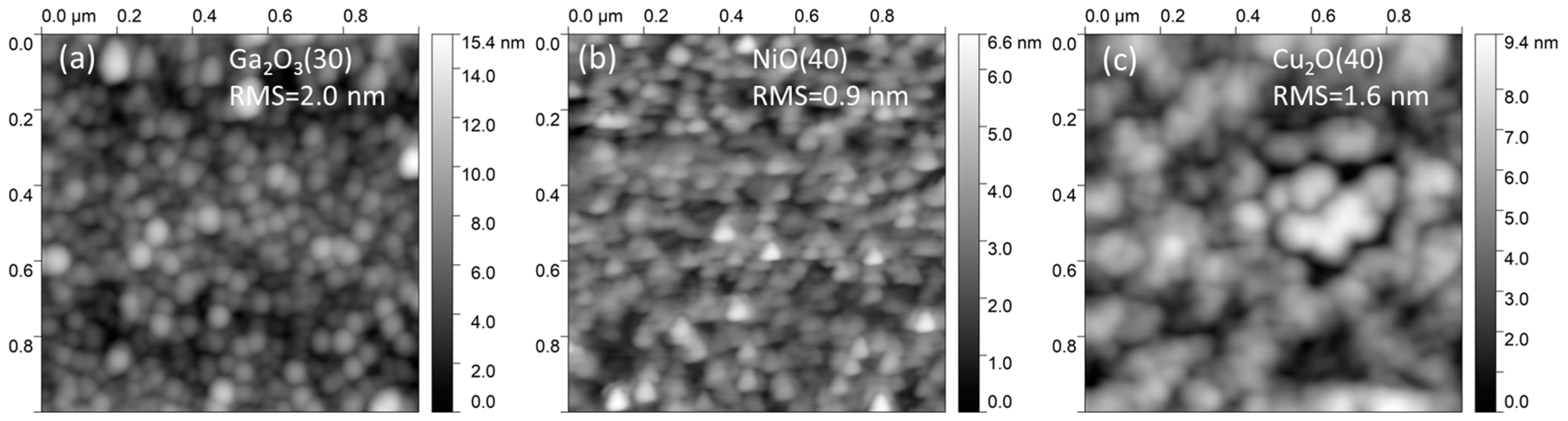
Abstract
:1. Introduction
2. Materials and Methods
3. Results
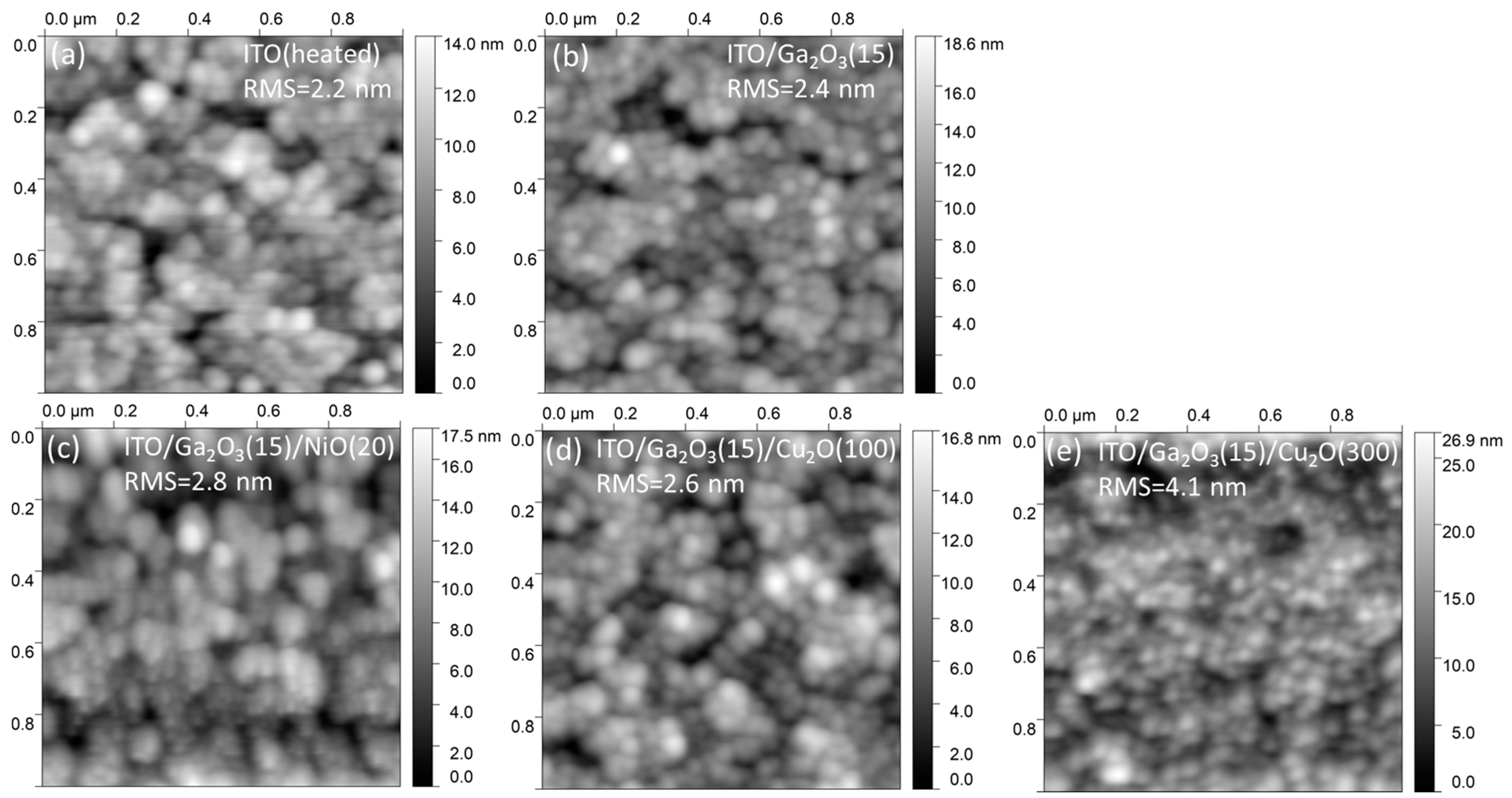
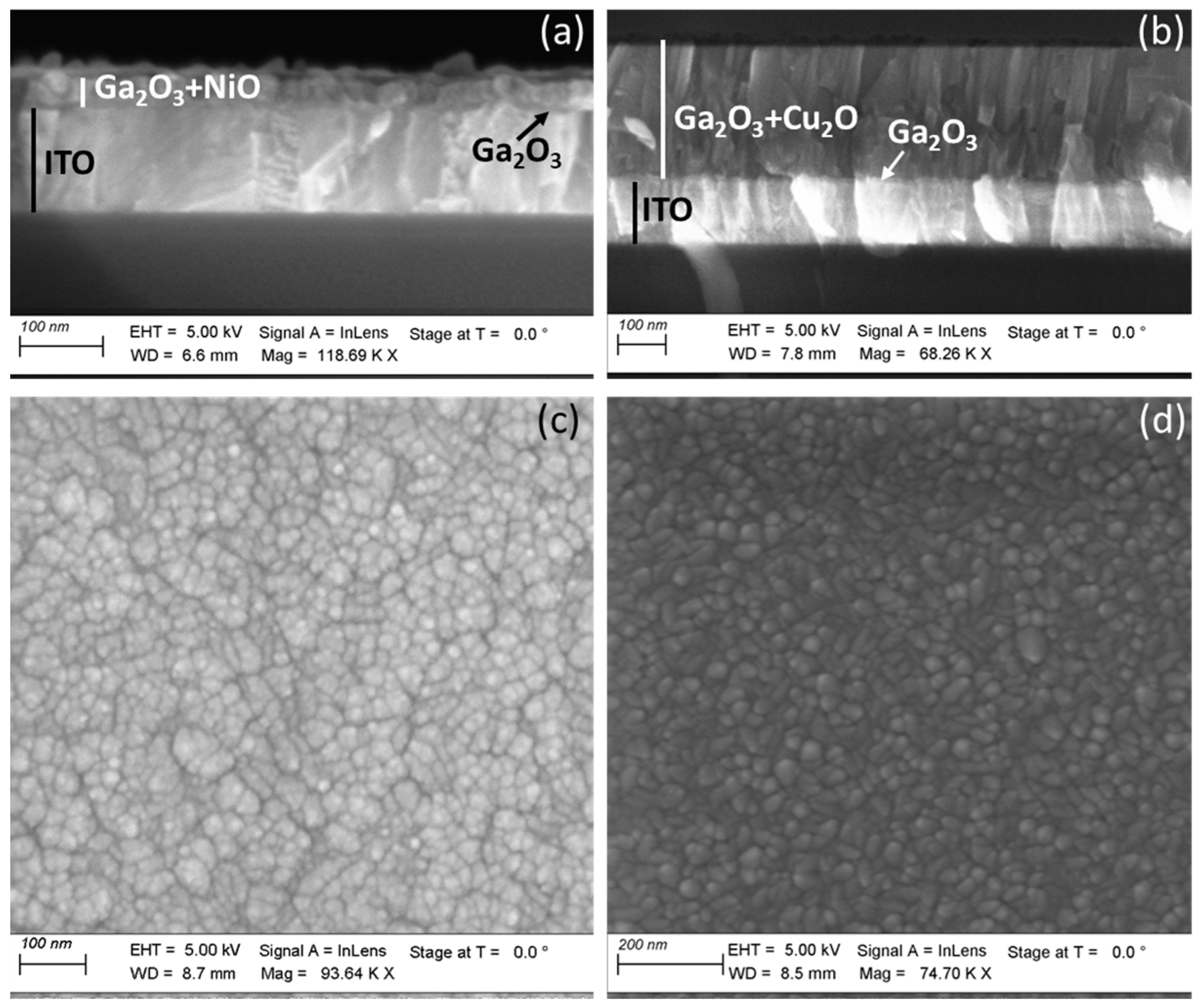
3.1. AFM and SEM Characterization
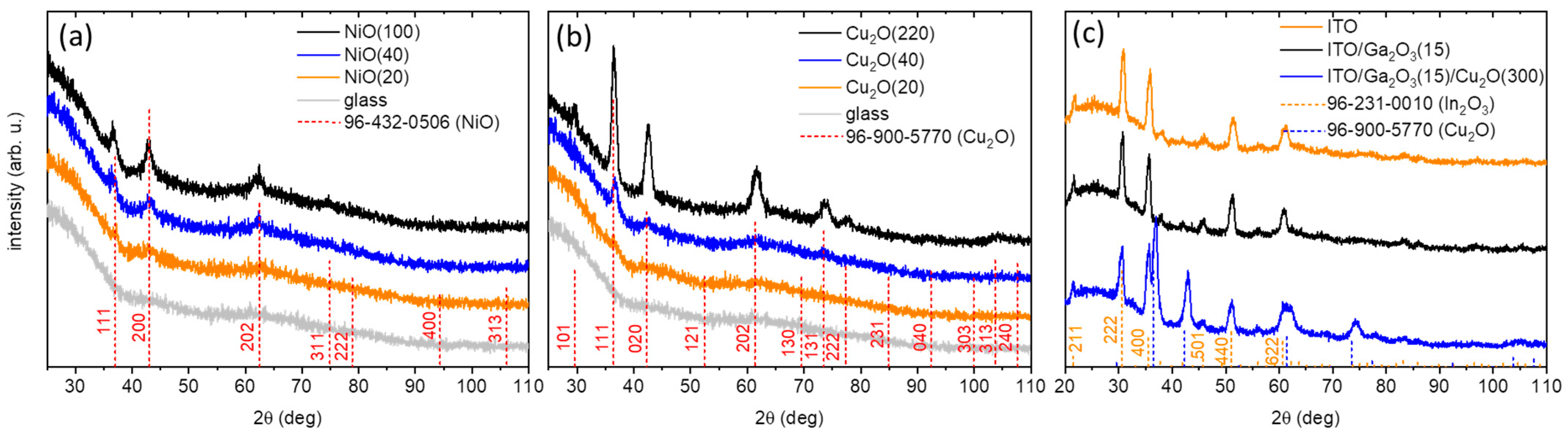
3.2. Structural Characterization
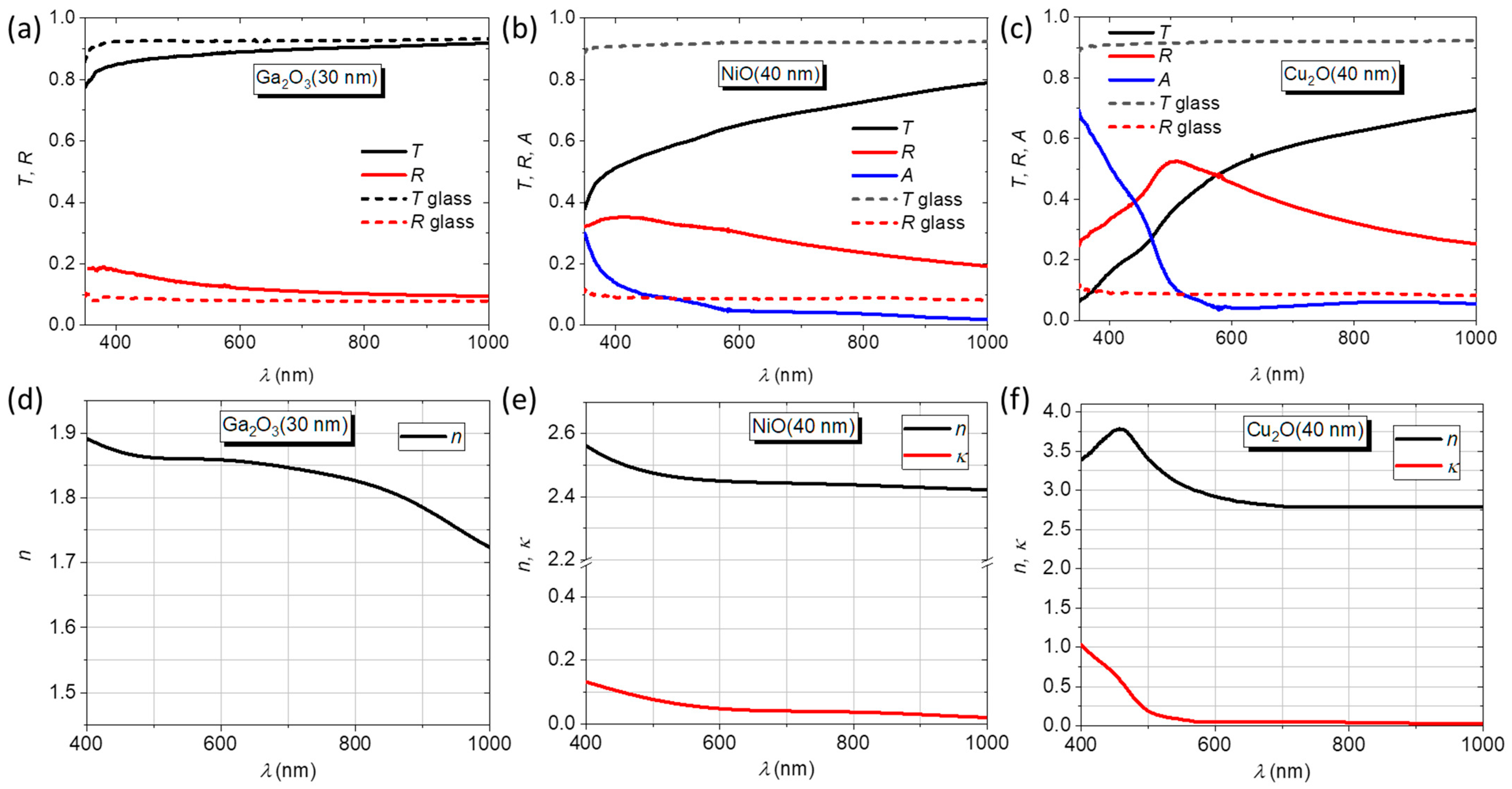
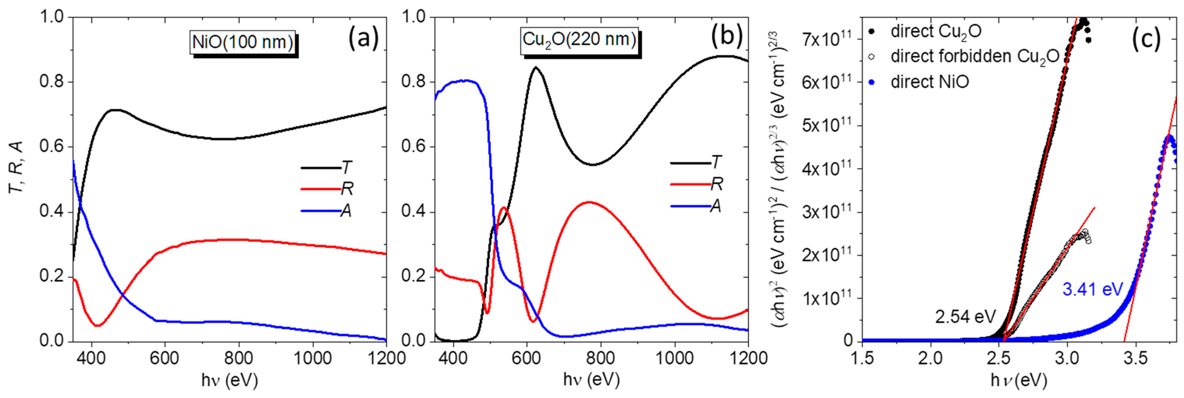
3.3. Optical Characterization
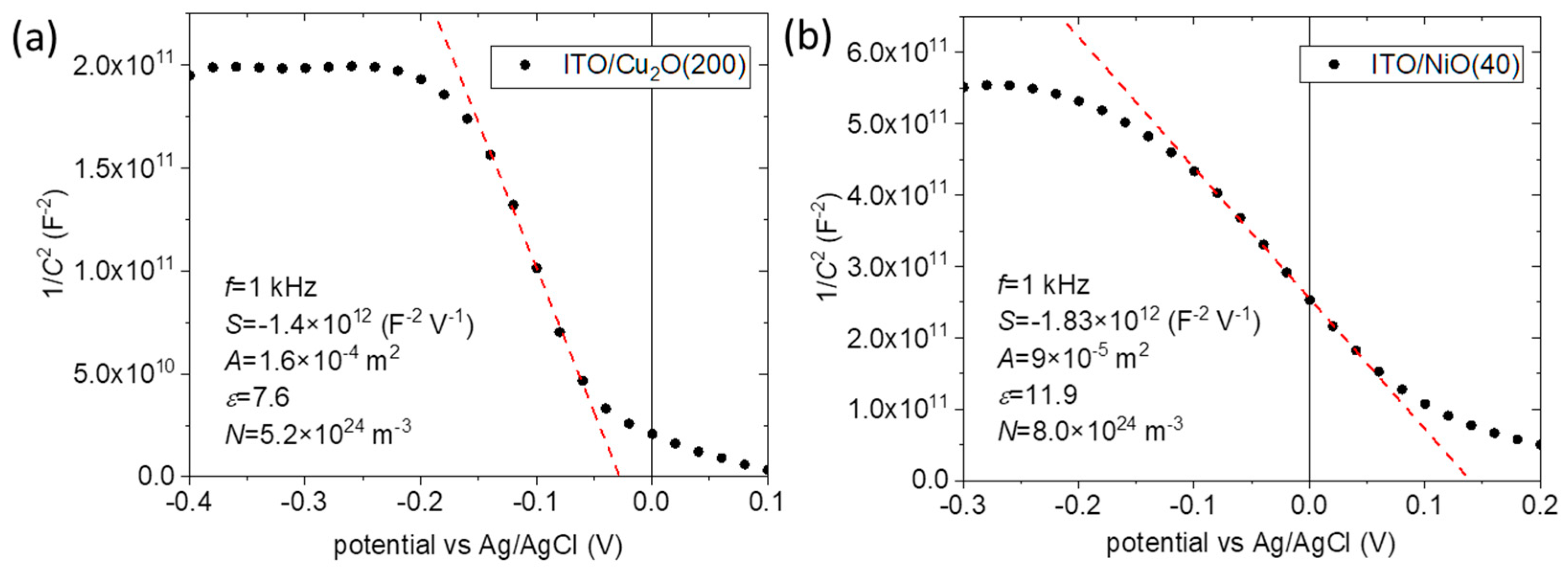
3.4. Electronic Properties Characterization
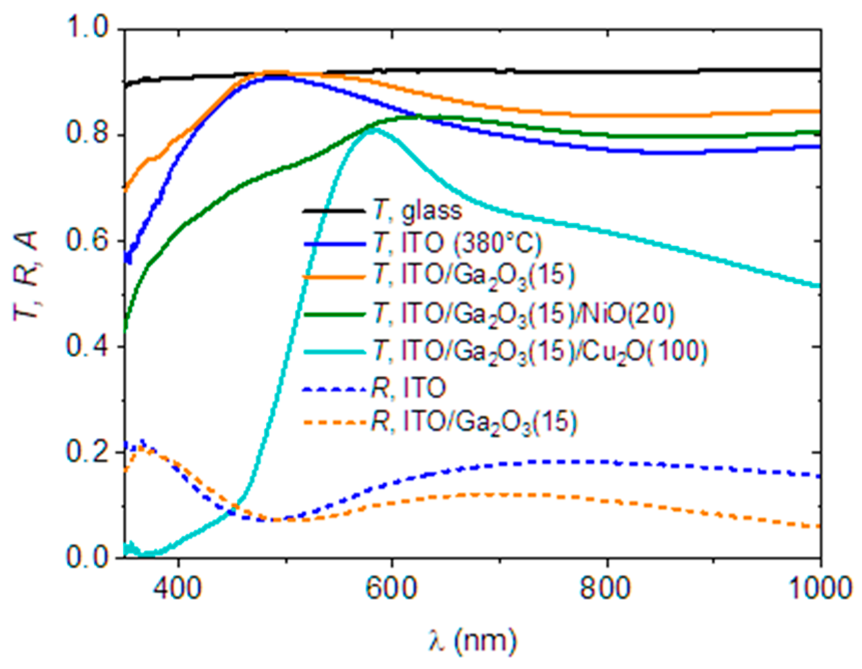
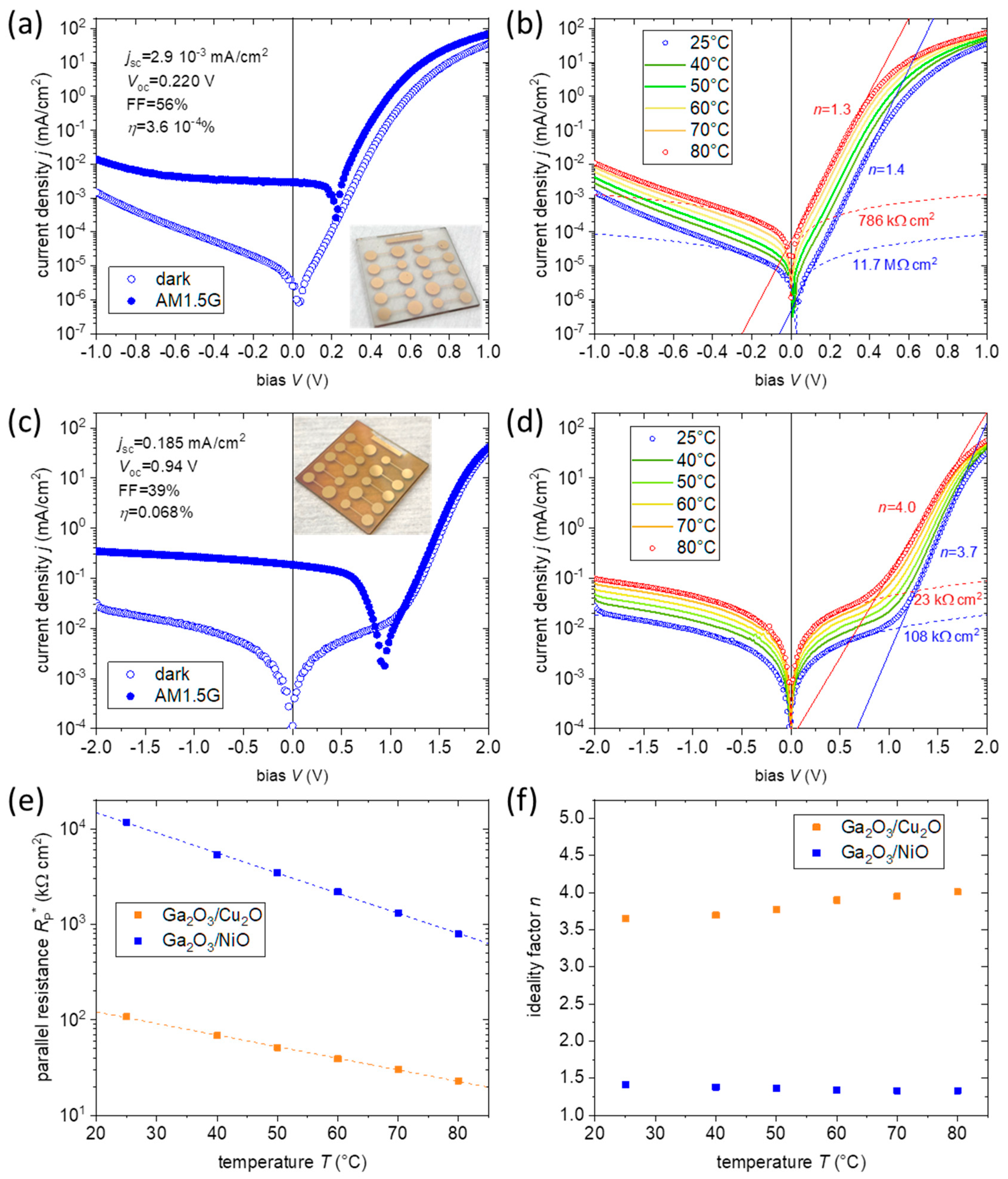
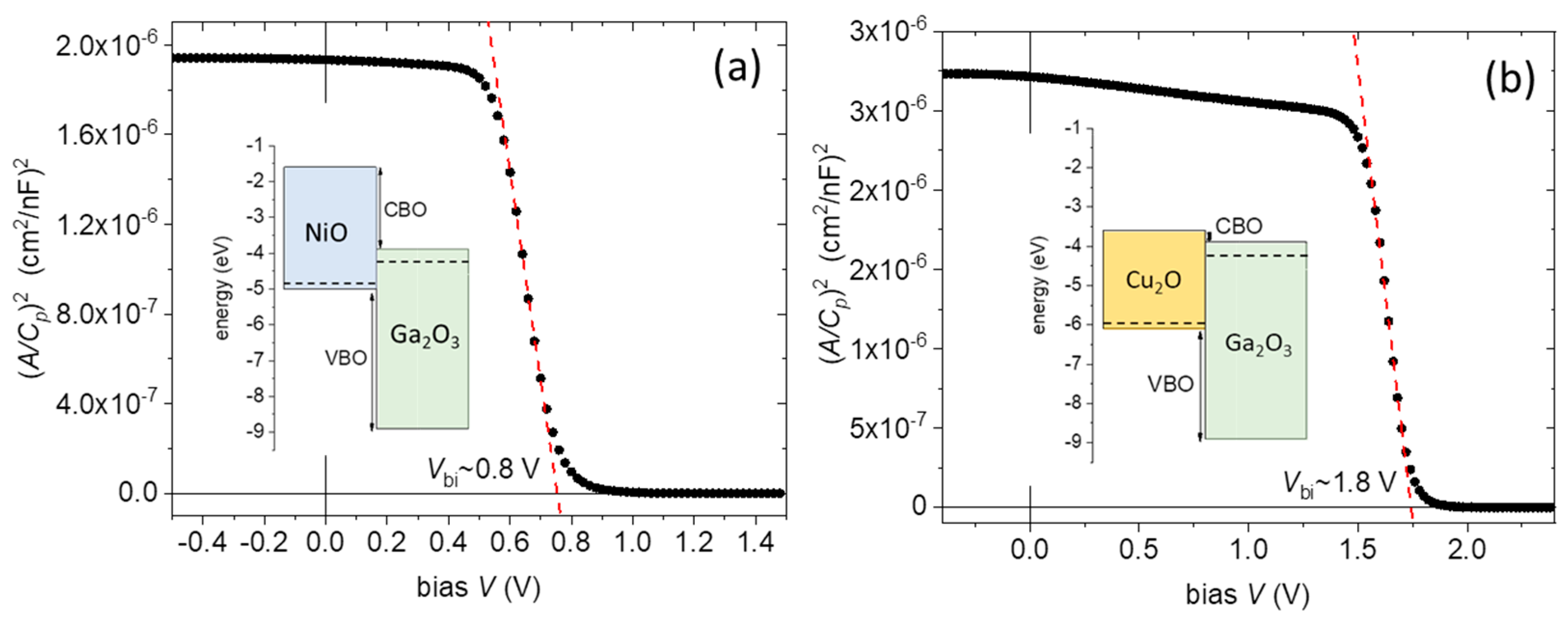
3.5. Heterojunction Charaterization
4. Conclusions
Supplementary Materials
Author Contributions
Funding
Data Availability Statement
Conflicts of Interest
References
- Cai, X.; Hu, T.; Hou, H.; Zhu, P.; Liu, R.; Peng, J.; Luo, W.; Yu, H. A review for nickel oxide hole transport layer and its application in halide perovskite solar cells. Mater. Today Sustain. 2023, 23, 100438. [Google Scholar] [CrossRef]
- Alkarsifi, R.; Ackermann, J.; Margeat, O. Hole transport layers in organic solar cells: A review. J. Met. Mater. Miner. 2022, 32, 1–22. [Google Scholar] [CrossRef]
- Park, H.; Chaurasiya, R.; Jeong, B.H.; Sakthivel, P.; Park, H.J. Nickel Oxide for Perovskite Photovoltaic Cells. Adv. Photonics Res. 2021, 2, 2000178. [Google Scholar] [CrossRef]
- Boyd, C.C.; Shallcross, R.C.; Moot, T.; Kerner, R.; Bertoluzzi, L.; Onno, A.; Kavadiya, S.; Chosy, C.; Wolf, E.J.; Werner, J.; et al. Overcoming Redox Reactions at Perovskite-Nickel Oxide Interfaces to Boost Voltages in Perovskite Solar Cells. Joule 2020, 4, 1759–1775. [Google Scholar] [CrossRef]
- Di Girolamo, D.; Di Giacomo, F.; Matteocci, F.; Marrani, A.G.; Dini, D.; Abate, A. Progress, highlights and perspectives on NiO in perovskite photovoltaics. Chem. Sci. 2020, 11, 7746–7759. [Google Scholar] [CrossRef]
- Chatterjee, S.; Pal, A.J. Introducing Cu2O Thin Films as a Hole-Transport Layer in Efficient Planar Perovskite Solar Cell Structures. J. Phys. Chem. C 2016, 120, 1428–1437. [Google Scholar] [CrossRef]
- Chuang, T.-H.; Chen, Y.-H.; Sakalley, S.; Cheng, W.-C.; Chan, C.K.; Chen, C.-P.; Chen, S.-C. Highly Stable and Enhanced Performance of p–i–n Perovskite Solar Cells via Cuprous Oxide Hole-Transport Layers. Nanomaterials 2023, 13, 1363. [Google Scholar] [CrossRef] [PubMed]
- Dimopoulos, T. All-Oxide Solar Cells. In The Future of Semiconductor Oxides in Next-Generation Solar Cells; Elsevier: Amsterdam, The Netherlands, 2018; pp. 439–480. ISBN 978-0-12-811165-9. [Google Scholar]
- Pan, L.; Liu, Y.; Yao, L.; Ren, D.; Sivula, K.; Grätzel, M.; Hagfeldt, A. Cu2O photocathodes with band-tail states assisted hole transport for standalone solar water splitting. Nat. Commun. 2020, 11, 318. [Google Scholar] [CrossRef] [PubMed]
- Hu, K.-H.; Wang, Z.-K.; Wang, K.-L.; Zhuo, M.-P.; Zhang, Y.; Igbari, F.; Ye, Q.-Q.; Liao, L.-S. γ-Ga2O3 Nanocrystals Electron-Transporting Layer for High-Performance Perovskite Solar Cells. Sol. RRL 2019, 3, 1900201. [Google Scholar] [CrossRef]
- Lu, X.; Deng, Y.; Pei, Y.; Chen, Z.; Wang, G. Recent advances in NiO/Ga2O3 heterojunctions for power electronics. J. Semicond. 2023, 44, 061802. [Google Scholar] [CrossRef]
- Kokubun, Y.; Kubo, S.; Nakagomi, S. All-oxide p–n heterojunction diodes comprising p-type NiO and n-type β-Ga2O3. Appl. Phys. Express 2016, 9, 091101. [Google Scholar] [CrossRef]
- Tadjer, M.J.; Luna, L.E.; Cleveland, E.; Hobart, K.D.; Kub, F.J. (Invited) Fabrication and Characterization of β-Ga2O3 Heterojunction Rectifiers. ECS Trans. 2018, 85, 21–26. [Google Scholar] [CrossRef]
- Lu, X.; Zhou, X.; Jiang, H.; Ng, K.W.; Chen, Z.; Pei, Y.; Lau, K.M.; Wang, G. 1-kV Sputtered p-NiO/n-Ga2O3 Heterojunction Diodes with an Ultra-Low Leakage Current Below 1 µA/cm2. IEEE Electron Device Lett. 2020, 41, 449–452. [Google Scholar] [CrossRef]
- Gong, H.; Chen, X.; Xu, Y.; Chen, Y.; Ren, F.; Liu, B.; Gu, S.; Zhang, R.; Ye, J. Band Alignment and Interface Recombination in NiO/β-Ga2O3 Type-II p-n Heterojunctions. IEEE Trans. Electron Devices 2020, 67, 3341–3347. [Google Scholar] [CrossRef]
- Wang, Y.; Wu, C.; Guo, D.; Li, P.; Wang, S.; Liu, A.; Li, C.; Wu, F.; Tang, W. All-Oxide NiO/Ga2O3 p–n Junction for Self-Powered UV Photodetector. ACS Appl. Electron. Mater. 2020, 2, 2032–2038. [Google Scholar] [CrossRef]
- Zhang, J.; Han, S.; Cui, M.; Xu, X.; Li, W.; Xu, H.; Jin, C.; Gu, M.; Chen, L.; Zhang, K.H.L. Fabrication and Interfacial Electronic Structure of Wide Bandgap NiO and Ga2O3 p–n Heterojunction. ACS Appl. Electron. Mater. 2020, 2, 456–463. [Google Scholar] [CrossRef]
- Minami, T.; Nishi, Y.; Miyata, T. High-Efficiency Cu2O-Based Heterojunction Solar Cells Fabricated Using a Ga2O3 Thin Film as N-Type Layer. Appl. Phys. Express 2013, 6, 044101. [Google Scholar] [CrossRef]
- Lee, Y.S.; Chua, D.; Brandt, R.E.; Siah, S.C.; Li, J.V.; Mailoa, J.P.; Lee, S.W.; Gordon, R.G.; Buonassisi, T. Atomic Layer Deposited Gallium Oxide Buffer Layer Enables 1.2 V Open-Circuit Voltage in Cuprous Oxide Solar Cells. Adv. Mater. 2014, 26, 4704–4710. [Google Scholar] [CrossRef] [PubMed]
- Chua, D.; Kim, S.B.; Gordon, R. Enhancement of the open circuit voltage of Cu2O/Ga2O3 heterojunction solar cells through the mitigation of interfacial recombination. AIP Adv. 2019, 9, 055203. [Google Scholar] [CrossRef]
- Benz, S.L.; Becker, M.; Polity, A.; Chatterjee, S.; Klar, P.J. Determining the band alignment of copper-oxide gallium-oxide heterostructures. J. Appl. Phys. 2021, 129, 115305. [Google Scholar] [CrossRef]
- Winkler, N.; Wibowo, R.A.; Kautek, W.; Ligorio, G.; List-Kratochvil, E.J.W.; Dimopoulos, T. Nanocrystalline Ga2O3 films deposited by spray pyrolysis from water-based solutions on glass and TCO substrates. J. Mater. Chem. C 2019, 7, 69–77. [Google Scholar] [CrossRef]
- Ebner, D.; Bauch, M.; Dimopoulos, T. High performance and low cost transparent electrodes based on ultrathin Cu layer. Opt. Express 2017, 25, A240. [Google Scholar] [CrossRef]
- Salunkhe, P.; AV, M.A.; Kekuda, D. Structural, spectroscopic and electrical properties of dc magnetron sputtered NiO thin films and an insight into different defect states. Appl. Phys. A 2021, 127, 390. [Google Scholar] [CrossRef]
- Potlog, T.; Ghimpu, L.; Suman, V.; Pantazi, A.; Enachescu, M. Influence of RF sputtering power and thickness on structural and optical properties of NiO thin films. Mater. Res. Express 2019, 6, 096440. [Google Scholar] [CrossRef]
- Lee, H.; Huang, Y.-T.; Horn, M.W.; Feng, S.-P. Engineered optical and electrical performance of rf–sputtered undoped nickel oxide thin films for inverted perovskite solar cells. Sci. Rep. 2018, 8, 5590. [Google Scholar] [CrossRef]
- Dolai, S.; Das, S.; Hussain, S.; Bhar, R.; Pal, A.K. Cuprous oxide (Cu2O) thin films prepared by reactive d.c. sputtering technique. Vacuum 2017, 141, 296–306. [Google Scholar] [CrossRef]
- Azanza Ricardo, C.L.; D’Incau, M.; Leoni, M.; Malerba, C.; Mittiga, A.; Scardi, P. Structural properties of RF-magnetron sputtered Cu2O thin films. Thin Solid Film. 2011, 520, 280–286. [Google Scholar] [CrossRef]
- Bordun, O.M.; Kukharskyy, I.Y.; Bordun, B.O.; Lushchanets, V.B. Dispersion of Refractive Index of β-Ga2O3 Thin Films. J. Appl. Spectrosc. 2014, 81, 771–775. [Google Scholar] [CrossRef]
- Mahmoodinezhad, A.; Janowitz, C.; Naumann, F.; Plate, P.; Gargouri, H.; Henkel, K.; Schmeißer, D.; Flege, J.I. Low-temperature growth of gallium oxide thin films by plasma-enhanced atomic layer deposition. J. Vac. Sci. Technol. A 2020, 38, 022404. [Google Scholar] [CrossRef]
- Park, J.-W.; Choi, K.N.; Baek, S.H.; Chung, K.S.; Lee, H. Optical Properties of NiO Thin Films Grown by Using Sputtering Deposition and Studied with Spectroscopic Ellipsometry. J. Korean Phy. Soc. 2008, 52, 1868–1876. [Google Scholar] [CrossRef]
- Ito, T.; Kawashima, T.; Yamaguchi, H.; Masumi, T.; Adachi, S. Optical Properties of Cu2O Studied by Spectroscopic Ellipsometry. J. Phys. Soc. Jpn. 1998, 67, 2125–2131. [Google Scholar] [CrossRef]
- Tauc, J. Optical properties and electronic structure of amorphous Ge and Si. Mater. Res. Bull. 1968, 3, 37–46. [Google Scholar] [CrossRef]
- Ruske, F.; Wimmer, M.; Köppel, G.; Pflug, A.; Rech, B. Optical Characterization of High Mobility Polycrystalline ZnO:Al Films; Rogers, D.J., Ed.; SPIE OPTO: San Francisco, CA, USA, 2012; p. 826303. [Google Scholar]
- Wang, Y.; Bruyère, S.; Kumagai, Y.; Tsunoda, N.; Oba, F.; Ghanbaja, J.; Sun, H.; Dai, B.; Pierson, J.-F. Tuning the optical band gap and electrical properties of NiO thin films by nitrogen doping: A joint experimental and theoretical study. RSC Adv. 2022, 12, 21940–21945. [Google Scholar] [CrossRef]
- Predanocy, M.; Hotový, I.; Čaplovičová, M. Structural, optical and electrical properties of sputtered NiO thin films for gas detection. Appl. Surf. Sci. 2017, 395, 208–213. [Google Scholar] [CrossRef]
- Terlemezoglu, M.; Surucu, O.; Isik, M.; Gasanly, N.M.; Parlak, M. Temperature-dependent optical characteristics of sputtered NiO thin films. Appl. Phys. A 2022, 128, 50. [Google Scholar] [CrossRef]
- Malerba, C.; Biccari, F.; Leonor Azanza Ricardo, C.; D’Incau, M.; Scardi, P.; Mittiga, A. Absorption coefficient of bulk and thin film Cu2O. Sol. Energy Mater. Sol. Cells 2011, 95, 2848–2854. [Google Scholar] [CrossRef]
- Lee, S.H. The Characteristics of Cu2O Thin Films Deposited Using RF-Magnetron Sputtering Method with Nitrogen-Ambient. ETRI J. 2013, 35, 1156–1159. [Google Scholar] [CrossRef]
- Wang, Y.; Miska, P.; Pilloud, D.; Horwat, D.; Mücklich, F.; Pierson, J.F. Transmittance enhancement and optical band gap widening of Cu 2 O thin films after air annealing. J. Appl. Phys. 2014, 115, 073505. [Google Scholar] [CrossRef]
- Islam, M.A.; Wahab, Y.A.; Khandaker, M.U.; Alsubaie, A.; Almalki, A.S.A.; Bradley, D.A.; Amin, N. High Mobility Reactive Sputtered CuxO Thin Film for Highly Efficient and Stable Perovskite Solar Cells. Crystals 2021, 11, 389. [Google Scholar] [CrossRef]
- Deuermeier, J.; Liu, H.; Rapenne, L.; Calmeiro, T.; Renou, G.; Martins, R.; Muñoz-Rojas, D.; Fortunato, E. Visualization of nanocrystalline CuO in the grain boundaries of Cu2O thin films and effect on band bending and film resistivity. APL Mater. 2018, 6, 096103. [Google Scholar] [CrossRef]
- Young, K.F.; Frederikse, H.P.R. Compilation of the Static Dielectric Constant of Inorganic Solids. J. Phys. Chem. Ref. Data 1973, 2, 313–410. [Google Scholar] [CrossRef]
- Zhang, L.; McMillon, L.; McNatt, J. Gas-dependent bandgap and electrical conductivity of Cu2O thin films. Sol. Energy Mater. Sol. Cells 2013, 108, 230–234. [Google Scholar] [CrossRef]
- Sah, C.; Noyce, R.; Shockley, W. Carrier Generation and Recombination in P-N Junctions and P-N Junction Characteristics. Proc. IRE 1957, 45, 1228–1243. [Google Scholar] [CrossRef]
- Banerjee, S.; Anderson, W.A. Temperature dependence of shunt resistance in photovoltaic devices. Appl. Phys. Lett. 1986, 49, 38–40. [Google Scholar] [CrossRef]
- Shah, J.M.; Li, Y.-L.; Gessmann, T.; Schubert, E.F. Experimental analysis and theoretical model for anomalously high ideality factors (n ≫ 2.0) in AlGaN/GaN p-n junction diodes. J. Appl. Phys. 2003, 94, 2627–2630. [Google Scholar] [CrossRef]
- Breitenstein, O.; Bauer, J.; Lotnyk, A.; Wagner, J.-M. Defect induced non-ideal dark—Characteristics of solar cells. Superlattices Microstruct. 2009, 45, 182–189. [Google Scholar] [CrossRef]
- Jeong, S.; Song, S.H.; Nagaich, K.; Campbell, S.A.; Aydil, E.S. An analysis of temperature dependent current–voltage characteristics of Cu2O–ZnO heterojunction solar cells. Thin Solid Film. 2011, 519, 6613–6619. [Google Scholar] [CrossRef]
- Xiong, C.; Sun, J.; Yang, H.; Jiang, H. Real reason for high ideality factor in organic solar cells: Energy disorder. Sol. Energy 2019, 178, 193–200. [Google Scholar] [CrossRef]
- Mahapatra, A.; Parikh, N.; Kumar, P.; Kumar, M.; Prochowicz, D.; Kalam, A.; Tavakoli, M.M.; Yadav, P. Changes in the Electrical Characteristics of Perovskite Solar Cells with Aging Time. Molecules 2020, 25, 2299. [Google Scholar] [CrossRef] [PubMed]
- Kaminski, A.; Marchand, J.J.; El Omari, H.; Laugier, A.; Le, Q.N.; Sarti, D. Conduction processes in silicon solar cells. In Proceedings of the Conference Record of the Twenty Fifth IEEE Photovoltaic Specialists Conference, Washington, DC, USA, 13–17 May 1996; IEEE: Washington, DC, USA, 1996; pp. 573–576. [Google Scholar]
- Breitenstein, O.; Bauer, J.; Altermatt, P.P.; Ramspeck, K. Influence of Defects on Solar Cell Characteristics. Solid State Phenom. 2009, 156–158, 1–10. [Google Scholar] [CrossRef]
- Carey, P.H.; Yang, J.; Ren, F.; Hays, D.C.; Pearton, S.J.; Kuramata, A.; Kravchenko, I.I. Improvement of Ohmic contacts on Ga2O3 through use of ITO-interlayers. J. Vac. Sci. Technol. B 2017, 35, 061201. [Google Scholar] [CrossRef]
- Xia, X.; Xian, M.; Ren, F.; Rasel, M.A.J.; Haque, A.; Pearton, S.J. Thermal Stability of Transparent ITO/n-Ga2O3/n+-Ga2O3/ITO Rectifiers. ECS J. Solid State Sci. Technol. 2021, 10, 115005. [Google Scholar] [CrossRef]
- Tuğluoğlu, N.; Karadeniz, S.; Birkan Selçuk, A.; Bilge Ocak, S. Effect of oxide thickness on the capacitance and conductance characteristics of MOS structures. Phys. B Condens. Matter 2007, 400, 168–174. [Google Scholar] [CrossRef]
- Zhang, X.; Zhu, H.; Cheng, C.; Yu, T.; Zhang, D.; Zhong, H.; Li, X.; Cheng, Y.; Xu, X.; Cheng, L.; et al. Single frequency correction based on three-element model for thin dielectric MOS capacitor. Solid-State Electron. 2017, 129, 97–102. [Google Scholar] [CrossRef]


Disclaimer/Publisher’s Note: The statements, opinions and data contained in all publications are solely those of the individual author(s) and contributor(s) and not of MDPI and/or the editor(s). MDPI and/or the editor(s) disclaim responsibility for any injury to people or property resulting from any ideas, methods, instructions or products referred to in the content. |
© 2024 by the authors. Licensee MDPI, Basel, Switzerland. This article is an open access article distributed under the terms and conditions of the Creative Commons Attribution (CC BY) license (https://creativecommons.org/licenses/by/4.0/).
Share and Cite
Dimopoulos, T.; Wibowo, R.A.; Edinger, S.; Wolf, M.; Fix, T. Heterojunction Devices Fabricated from Sprayed n-Type Ga2O3, Combined with Sputtered p-Type NiO and Cu2O. Nanomaterials 2024, 14, 300. https://doi.org/10.3390/nano14030300
Dimopoulos T, Wibowo RA, Edinger S, Wolf M, Fix T. Heterojunction Devices Fabricated from Sprayed n-Type Ga2O3, Combined with Sputtered p-Type NiO and Cu2O. Nanomaterials. 2024; 14(3):300. https://doi.org/10.3390/nano14030300
Chicago/Turabian StyleDimopoulos, Theodoros, Rachmat Adhi Wibowo, Stefan Edinger, Maximilian Wolf, and Thomas Fix. 2024. "Heterojunction Devices Fabricated from Sprayed n-Type Ga2O3, Combined with Sputtered p-Type NiO and Cu2O" Nanomaterials 14, no. 3: 300. https://doi.org/10.3390/nano14030300