
Lattice Thermal Conductivity of Monolayer InSe Calculated by Machine Learning Potential

Abstract
:1. Introduction
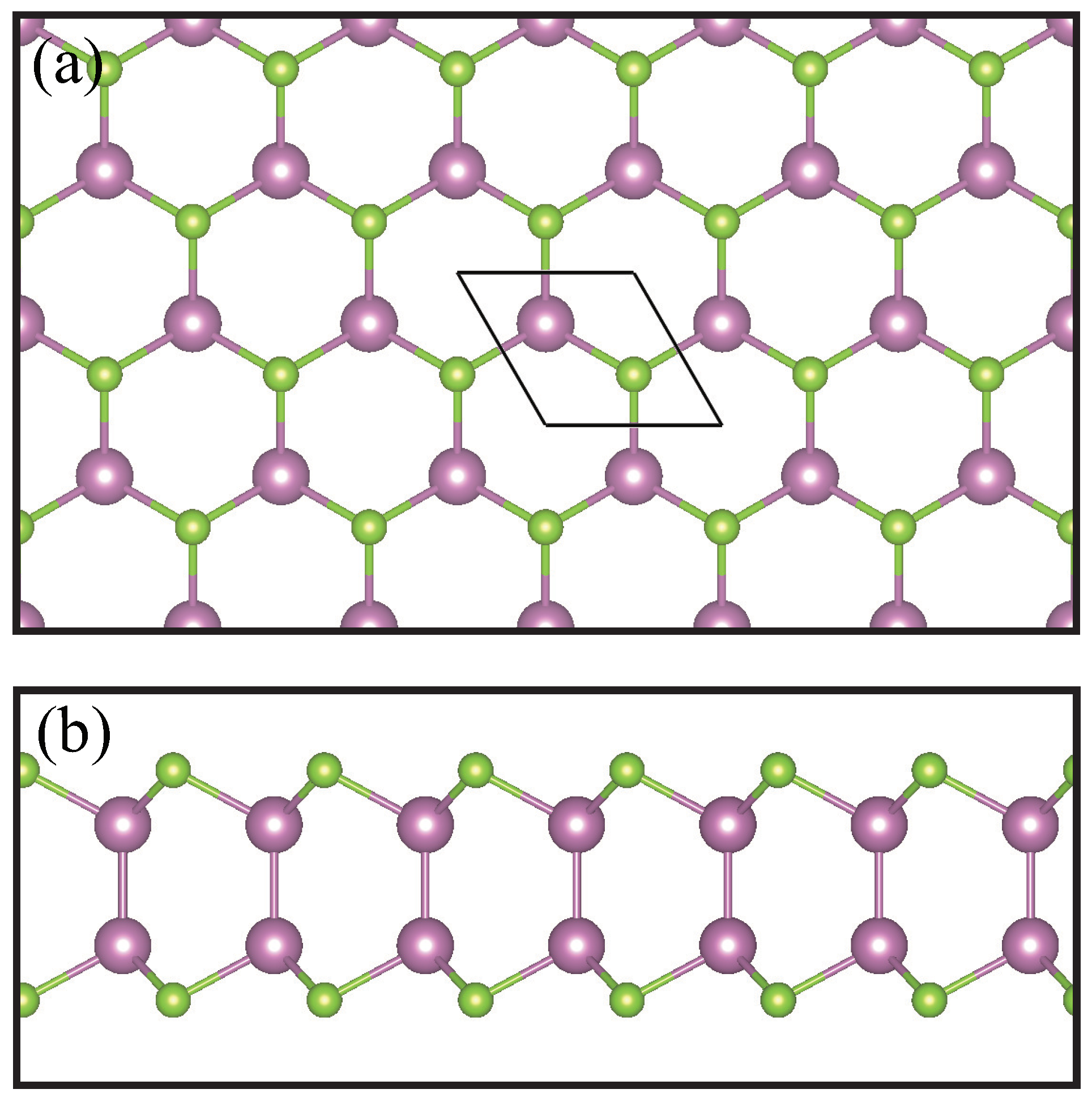
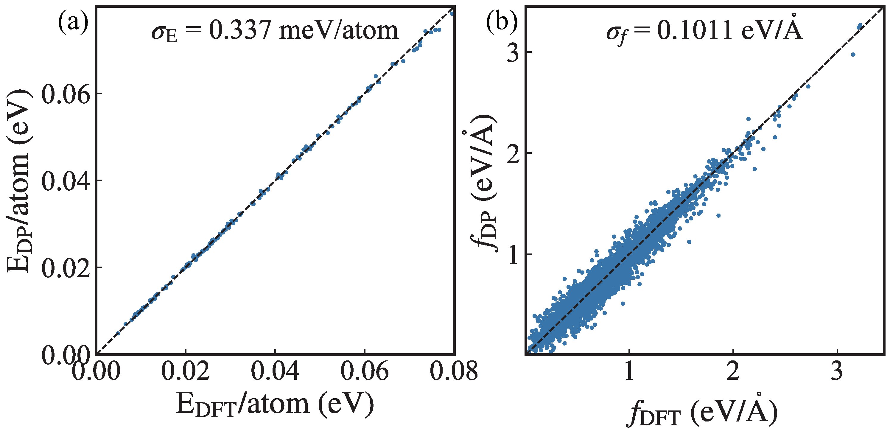
2. Methodology
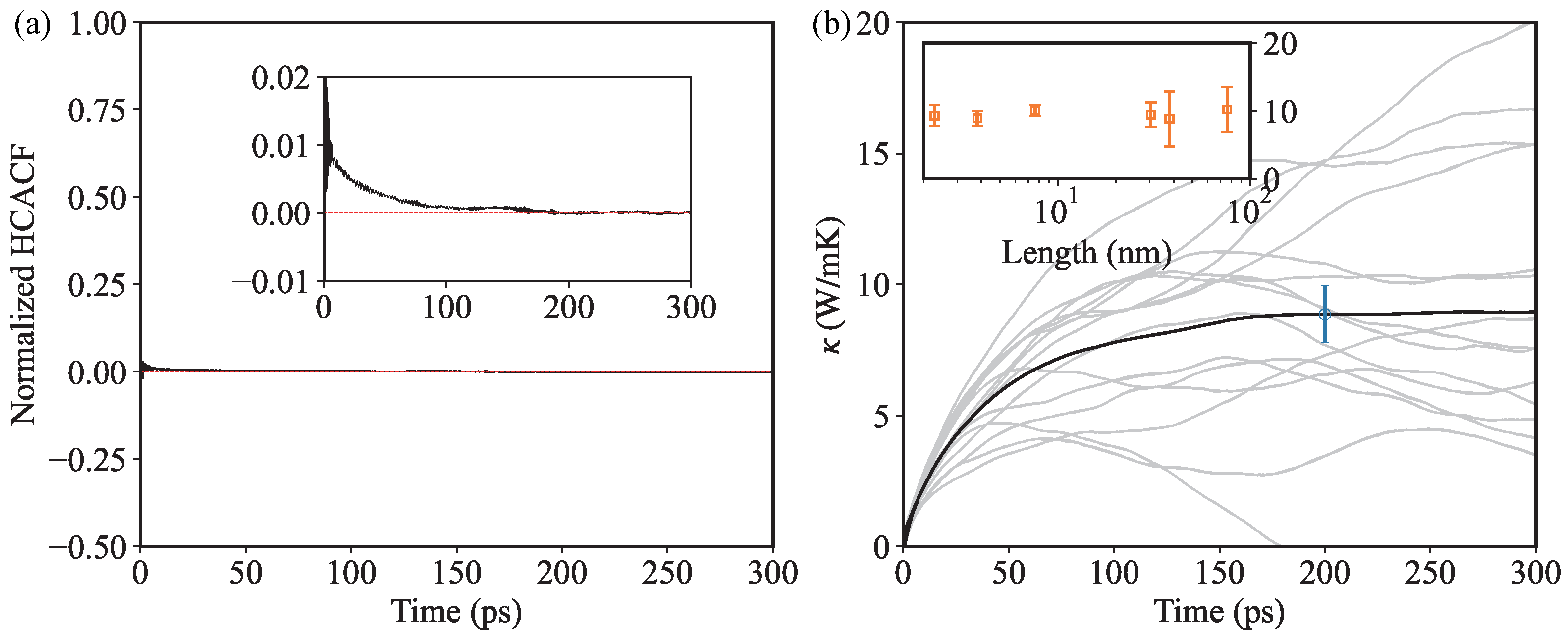
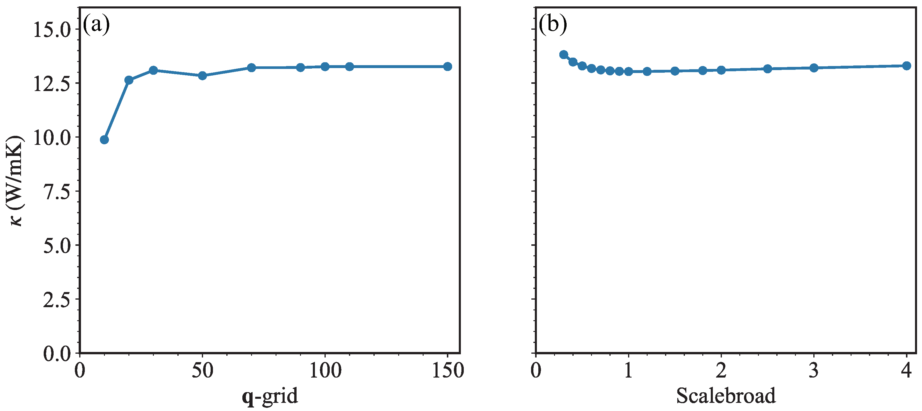
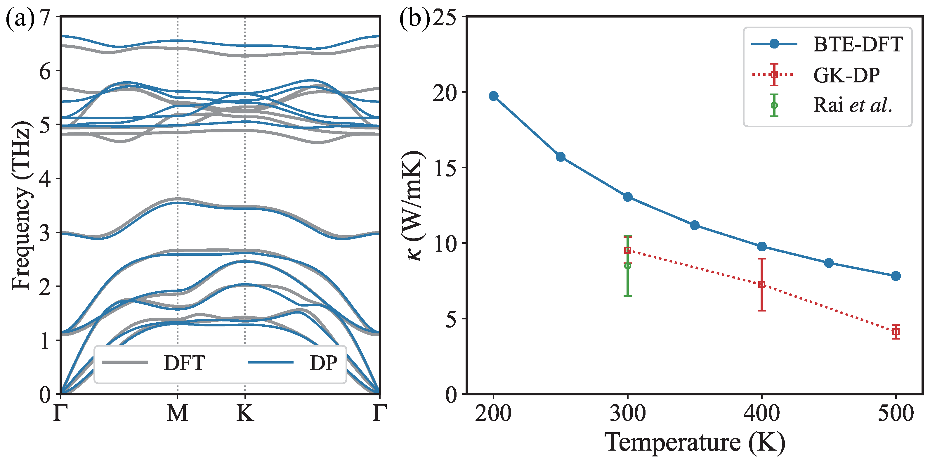
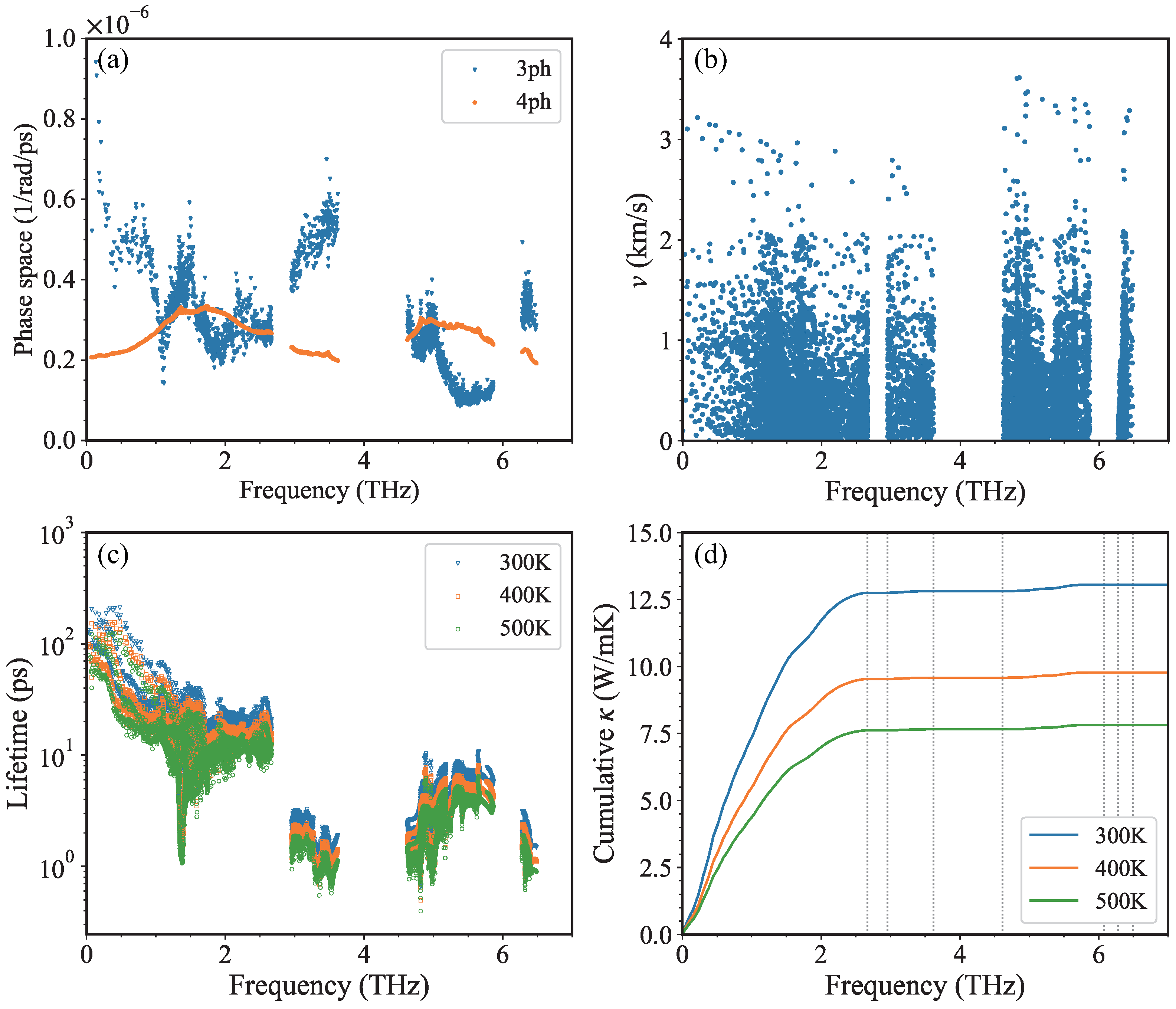
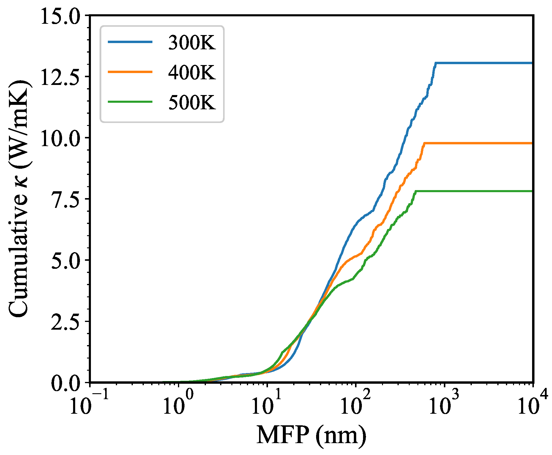
3. Results and Discussion
4. Conclusions
Author Contributions
Funding
Institutional Review Board Statement
Informed Consent Statement
Data Availability Statement
Conflicts of Interest
References
- Li, M.Y.; Su, S.K.; Wong, H.S.P.; Li, L.J. How 2D semiconductors could extend Moore’s law. Nature 2019, 567, 169–170. [Google Scholar] [CrossRef] [PubMed]
- Fiori, G.; Bonaccorso, F.; Iannaccone, G.; Palacios, T.; Neumaier, D.; Seabaugh, A.; Banerjee, S.K.; Colombo, L. Electronics based on two-dimensional materials. Nat. Nanotechnol. 2014, 9, 768–779. [Google Scholar] [CrossRef] [PubMed]
- Zhang, P.; Zhang, S.; Lai, K.; Lei, L.; Zheng, Z.; Kang, D.; Zhao, Z.; Dai, J. Strongly anisotropic ultrafast dynamic behavior of GaTe dominated by the tilted and flat bands. Nanotechnology 2023, 34, 285703. [Google Scholar] [CrossRef] [PubMed]
- Lai, K.; Ju, S.; Zhu, H.; Wang, H.; Wu, H.; Yang, B.; Zhang, E.; Yang, M.; Li, F.; Cui, S.; et al. Strong bulk-surface interaction dominated in-plane anisotropy of electronic structure in GaTe. Commun. Phys. 2022, 5, 143. [Google Scholar] [CrossRef]
- Lai, K.; Dai, J. Stacking effect on the electronic structures of hexagonal GaTe. J. Phys. D Appl. Phys. 2023, 56, 275301. [Google Scholar] [CrossRef]
- Song, C.; Fan, F.; Xuan, N.; Huang, S.; Zhang, G.; Wang, C.; Sun, Z.; Wu, H.; Yan, H. Largely Tunable Band Structures of Few-Layer InSe by Uniaxial Strain. ACS Appl. Mater. Interfaces 2018, 10, 3994–4000. [Google Scholar] [CrossRef] [PubMed]
- Segura, A.; Pomer, F.; Cantarero, A.; Krause, W.; Chevy, A. Electron scattering mechanisms in n-type indium selenide. Phys. Rev. B 1984, 29, 5708–5717. [Google Scholar] [CrossRef]
- Poncé, S.; Li, W.; Reichardt, S.; Giustino, F. First-principles calculations of charge carrier mobility and conductivity in bulk semiconductors and two-dimensional materials. Rep. Prog. Phys. 2020, 83, 036501. [Google Scholar] [CrossRef]
- Bandurin, D.A.; Tyurnina, A.V.; Yu, G.L.; Mishchenko, A.; Zólyomi, V.; Morozov, S.V.; Kumar, R.K.; Gorbachev, R.V.; Kudrynskyi, Z.R.; Pezzini, S.; et al. High electron mobility, quantum Hall effect and anomalous optical response in atomically thin InSe. Nat. Nanotechnol. 2017, 12, 223–227. [Google Scholar] [CrossRef]
- Ho, C.H.; Chu, Y.J. Bending Photoluminescence and Surface Photovoltaic Effect on Multilayer InSe 2D Microplate Crystals. Adv. Opt. Mater. 2015, 3, 1750–1758. [Google Scholar] [CrossRef]
- Lei, S.; Ge, L.; Najmaei, S.; George, A.; Kappera, R.; Lou, J.; Chhowalla, M.; Yamaguchi, H.; Gupta, G.; Vajtai, R.; et al. Evolution of the Electronic Band Structure and Efficient Photo-Detection in Atomic Layers of InSe. ACS Nano 2014, 8, 1263–1272. [Google Scholar] [CrossRef]
- Tamalampudi, S.R.; Lu, Y.Y.; U., R.K.; Sankar, R.; Liao, C.D.; B., K.M.; Cheng, C.H.; Chou, F.C.; Chen, Y.T. High Performance and Bendable Few-Layered InSe Photodetectors with Broad Spectral Response. Nano Lett. 2014, 14, 2800–2806. [Google Scholar] [CrossRef] [PubMed]
- Mudd, G.W.; Svatek, S.A.; Ren, T.; Patanè, A.; Makarovsky, O.; Eaves, L.; Beton, P.H.; Kovalyuk, Z.D.; Lashkarev, G.V.; Kudrynskyi, Z.R.; et al. Tuning the Bandgap of Exfoliated InSe Nanosheets by Quantum Confinement. Adv. Mater. 2013, 25, 5714–5718. [Google Scholar] [CrossRef]
- Rai, A.; Sangwan, V.K.; Gish, J.T.; Hersam, M.C.; Cahill, D.G. Anisotropic thermal conductivity of layered indium selenide. Appl. Phys. Lett. 2021, 118, 073101. [Google Scholar] [CrossRef]
- Li, K.; Hong, Y.; Li, Z.; Liu, X. Thermal property engineering of InSe layer by a thin Al2O3 stress liner. Appl. Phys. Lett. 2018, 113, 021903. [Google Scholar] [CrossRef]
- Buckley, D.; Kudrynskyi, Z.R.; Balakrishnan, N.; Vincent, T.; Mazumder, D.; Castanon, E.; Kovalyuk, Z.D.; Kolosov, O.; Kazakova, O.; Tzalenchuk, A.; et al. Anomalous Low Thermal Conductivity of Atomically Thin InSe Probed by Scanning Thermal Microscopy. Adv. Funct. Mater. 2021, 31, 2008967. [Google Scholar] [CrossRef]
- Pandey, T.; Parker, D.S.; Lindsay, L. Ab initio phonon thermal transport in monolayer InSe, GaSe, GaS, and alloys. Nanotechnology 2017, 28, 455706. [Google Scholar] [CrossRef] [PubMed]
- Nissimagoudar, A.S.; Rashid, Z.; Ma, J.; Li, W. Lattice Thermal Transport in Monolayer Group 13 Monochalcogenides MX (M = Ga, In; X = S, Se, Te): Interplay of Atomic Mass, Harmonicity, and Lone-Pair-Induced Anharmonicity. Inorg. Chem. 2020, 59, 14899–14909. [Google Scholar] [CrossRef] [PubMed]
- Nissimagoudar, A.S.; Ma, J.; Chen, Y.; Li, W. Thermal transport in monolayer InSe. J. Phys. Condens. Matter 2017, 29, 335702. [Google Scholar] [CrossRef]
- Majumdar, A.; Chowdhury, S.; Ahuja, R. Drastic reduction of thermal conductivity in hexagonal AX (A = Ga, In & Tl, X = S, Se & Te) monolayers due to alternative atomic configuration. Nano Energy 2021, 88, 106248. [Google Scholar] [CrossRef]
- Zeng, Z.; Li, S.; Tadano, T.; Chen, Y. Anharmonic lattice dynamics and thermal transport of monolayer InSe under equibiaxial tensile strains. J. Phys. Condens. Matter 2020, 32, 475702. [Google Scholar] [CrossRef] [PubMed]
- Chang, Z.; Yuan, K.; Sun, Z.; Zhang, X.; Gao, Y.; Qin, G.; Tang, D. Ultralow lattice thermal conductivity and dramatically enhanced thermoelectric properties of monolayer InSe induced by an external electric field. Phys. Chem. Chem. Phys. 2021, 23, 13633–13646. [Google Scholar] [CrossRef]
- Lindsay, L.; Broido, D.A.; Reinecke, T.L. First-Principles Determination of Ultrahigh Thermal Conductivity of Boron Arsenide: A Competitor for Diamond? Phys. Rev. Lett. 2013, 111, 025901. [Google Scholar] [CrossRef] [PubMed]
- Kang, J.S.; Li, M.; Wu, H.; Nguyen, H.; Hu, Y. Experimental observation of high thermal conductivity in boron arsenide. Science 2018, 361, 575–578. [Google Scholar] [CrossRef] [PubMed]
- Li, S.; Zheng, Q.; Lv, Y.; Liu, X.; Wang, X.; Huang, P.Y.; Cahill, D.G.; Lv, B. High thermal conductivity in cubic boron arsenide crystals. Science 2018, 361, 579–581. [Google Scholar] [CrossRef]
- Tian, F.; Song, B.; Chen, X.; Ravichandran, N.K.; Lv, Y.; Chen, K.; Sullivan, S.; Kim, J.; Zhou, Y.; Liu, T.H.; et al. Unusual high thermal conductivity in boron arsenide bulk crystals. Science 2018, 361, 582–585. [Google Scholar] [CrossRef]
- Feng, T.; Ruan, X. Four-phonon scattering reduces intrinsic thermal conductivity of graphene and the contributions from flexural phonons. Phys. Rev. B 2018, 97, 045202. [Google Scholar] [CrossRef]
- Zhou, W.; Dai, Y.; Zhang, J.; Song, B.; Liu, T.H.; Yang, R. Effect of four-phonon interaction on phonon thermal conductivity and mean-free-path spectrum of high-temperature phase SnSe. Appl. Phys. Lett. 2022, 121, 112202. [Google Scholar] [CrossRef]
- Zhang, E.; Yao, Y.; Gao, T.; Kang, D.; Wu, J.; Dai, J. The effect of external temperature gradients on thermal conductivity in non-equilibrium molecular dynamics simulations: From nanowires to bulk Si. J. Chem. Phys. 2019, 151, 064116. [Google Scholar] [CrossRef]
- Qiu, R.; Yu, X.; Wang, D.; Zhang, S.; Kang, D.; Dai, J. Nanoscale Topological Morphology Transition and Controllable Thermal Conductivity of Wrinkled Hexagonal Boron Nitride: Implications for Thermal Manipulation and Management. ACS Appl. Nano Mater. 2021, 4, 10665–10673. [Google Scholar] [CrossRef]
- Pham, V.T.; Fang, T.H. Effects of temperature and intrinsic structural defects on mechanical properties and thermal conductivities of InSe monolayers. Sci. Rep. 2020, 10, 15082. [Google Scholar] [CrossRef] [PubMed]
- Han, J.; Zhang, L.; Car, R.; E, W. Deep Potential: A General Representation of a Many-Body Potential Energy Surface. Commun. Comput. Phys. 2018, 23, 629–639. [Google Scholar] [CrossRef]
- Zhang, L.; Han, J.; Wang, H.; Car, R.; E, W. Deep Potential Molecular Dynamics: A Scalable Model with the Accuracy of Quantum Mechanics. Phys. Rev. Lett. 2018, 120, 143001. [Google Scholar] [CrossRef] [PubMed]
- Novikov, I.S.; Gubaev, K.; Podryabinkin, E.V.; Shapeev, A.V. The MLIP package: Moment tensor potentials with MPI and active learning. Mach. Learn. Sci. Technol. 2020, 2, 025002. [Google Scholar] [CrossRef]
- Zeng, Q.; Chen, B.; Yu, X.; Zhang, S.; Kang, D.; Wang, H.; Dai, J. Towards large-scale and spatiotemporally resolved diagnosis of electronic density of states by deep learning. Phys. Rev. B 2022, 105, 174109. [Google Scholar] [CrossRef]
- Li, R.; Lee, E.; Luo, T. A unified deep neural network potential capable of predicting thermal conductivity of silicon in different phases. Mater. Today Phys. 2020, 12, 100181. [Google Scholar] [CrossRef]
- Zeng, Q.; Yu, X.; Yao, Y.; Gao, T.; Chen, B.; Zhang, S.; Kang, D.; Wang, H.; Dai, J. Ab initio validation on the connection between atomistic and hydrodynamic description to unravel the ion dynamics of warm dense matter. Phys. Rev. Res. 2021, 3, 033116. [Google Scholar] [CrossRef]
- Mortazavi, B.; Podryabinkin, E.V.; Novikov, I.S.; Rabczuk, T.; Zhuang, X.; Shapeev, A.V. Accelerating first-principles estimation of thermal conductivity by machine-learning interatomic potentials: A MTP/ShengBTE solution. Comput. Phys. Commun. 2021, 258, 107583. [Google Scholar] [CrossRef]
- Mortazavi, B.; Novikov, I.S.; Podryabinkin, E.V.; Roche, S.; Rabczuk, T.; Shapeev, A.V.; Zhuang, X. Exploring phononic properties of two-dimensional materials using machine learning interatomic potentials. Appl. Mater. Today 2020, 20, 100685. [Google Scholar] [CrossRef]
- Liu, Z.; Yang, X.; Zhang, B.; Li, W. High Thermal Conductivity of Wurtzite Boron Arsenide Predicted by Including Four-Phonon Scattering with Machine Learning Potential. ACS Appl. Mater. Interfaces 2021, 13, 53409–53415. [Google Scholar] [CrossRef]
- Yang, F.; Zeng, Q.; Chen, B.; Kang, D.; Zhang, S.; Wu, J.; Yu, X.; Dai, J. Lattice Thermal Conductivity of MgSiO3 Perovskite and Post-Perovskite under Lower Mantle Conditions Calculated by Deep Potential Molecular Dynamics. Chin. Phys. Lett. 2022, 39, 116301. [Google Scholar] [CrossRef]
- Hu, T.; Zhou, J.; Dong, J. Strain induced new phase and indirect–direct band gap transition of monolayer InSe. Phys. Chem. Chem. Phys. 2017, 19, 21722–21728. [Google Scholar] [CrossRef] [PubMed]
- Sun, C.; Xiang, H.; Xu, B.; Xia, Y.; Yin, J.; Liu, Z. Ab initio study of carrier mobility of few-layer InSe. Appl. Phys. Express 2016, 9, 035203. [Google Scholar] [CrossRef]
- Wan, W.; Zhao, S.; Ge, Y.; Liu, Y. Phonon and electron transport in Janus monolayers based on InSe. J. Phys. Condens. Matter 2019, 31, 435501. [Google Scholar] [CrossRef]
- Wang, H.; Zhang, L.; Han, J.; Weinan, E. DeePMD-kit: A deep learning package for many-body potential energy representation and molecular dynamics. Comput. Phys. Commun. 2018, 228, 178–184. [Google Scholar] [CrossRef]
- Kresse, G.; Furthmüller, J. Efficiency of ab-initio total energy calculations for metals and semiconductors using a plane-wave basis set. Comput. Mater. Sci. 1996, 6, 15–50. [Google Scholar] [CrossRef]
- Kresse, G.; Furthmüller, J. Efficient iterative schemes for ab initio total-energy calculations using a plane-wave basis set. Phys. Rev. B 1996, 54, 11169–11186. [Google Scholar] [CrossRef]
- Zhang, L.; Lin, D.Y.; Wang, H.; Car, R.; Weinan, E. Active learning of uniformly accurate interatomic potentials for materials simulation. Phys. Rev. Mater. 2019, 3, 023804. [Google Scholar] [CrossRef]
- Perdew, J.P.; Burke, K.; Ernzerhof, M. Generalized Gradient Approximation Made Simple. Phys. Rev. Lett. 1996, 77, 3865–3868. [Google Scholar] [CrossRef]
- Blöchl, P.E. Projector augmented-wave method. Phys. Rev. B 1994, 50, 17953. [Google Scholar] [CrossRef]
- Holzwarth, N.; Tackett, A.; Matthews, G. A Projector Augmented Wave (PAW) code for electronic structure calculations, Part I: Atompaw for generating atom-centered functions. Comput. Phys. Commun. 2001, 135, 329–347. [Google Scholar] [CrossRef]
- Green, M. Markoff random processes and the statistical mechanics of time-dependent phenomena. J. Chem. Phys. 1952, 20, 1281–1295. [Google Scholar] [CrossRef]
- Kubo, R. Statistical-mechanical theory of irreversible processes. I. General theory and simple applications to magnetic and conduction problems. J. Phys. Soc. Jpn. 1957, 12, 570–586. [Google Scholar] [CrossRef]
- Plimpton, S. Fast parallel algorithms for short-range molecular dynamics. J. Comput. Phys. 1995, 117, 1–19. [Google Scholar] [CrossRef]
- Nosé, S. A unified formulation of the constant temperature molecular dynamics methods. J. Chem. Phys. 1984, 81, 511–519. [Google Scholar] [CrossRef]
- Hoover, W.G. Canonical dynamics: Equilibrium phase-space distributions. Phys. Rev. A 1985, 31, 1695. [Google Scholar] [CrossRef]
- Hohenberg, P.; Kohn, W. Inhomogeneous Electron Gas. Phys. Rev. 1964, 136, B864–B871. [Google Scholar] [CrossRef]
- Giannozzi, P.; Baroni, S.; Bonini, N.; Calandra, M.; Car, R.; Cavazzoni, C.; Ceresoli, D.; Chiarotti, G.L.; Cococcioni, M.; Dabo, I.; et al. QUANTUM ESPRESSO: A modular and open-source software project for quantum simulations of materials. J. Phys. Condens. Matter 2009, 21, 395502. [Google Scholar] [CrossRef]
- Giannozzi, P.; Andreussi, O.; Brumme, T.; Bunau, O.; Nardelli, M.B.; Calandra, M.; Colonna, N.; Carnimeo, I.; Dal Corso, A.; de Gironcoli, S.; et al. Advanced capabilities for materials modelling with Quantum ESPRESSO. J. Phys. Condens. Matter 2017, 29, 465901. [Google Scholar] [CrossRef]
- Hamann, D.R. Optimized norm-conserving Vanderbilt pseudopotentials. Phys. Rev. B 2013, 88, 085117. [Google Scholar] [CrossRef]
- Monkhorst, H.J.; Pack, J.D. Special points for Brillouin-zone integrations. Phys. Rev. B 1976, 13, 5188–5192. [Google Scholar] [CrossRef]
- Sohier, T.; Calandra, M.; Mauri, F. Density functional perturbation theory for gated two-dimensional heterostructures: Theoretical developments and application to flexural phonons in graphene. Phys. Rev. B 2017, 96, 075448. [Google Scholar] [CrossRef]
- Togo, A.; Tanaka, I. First principles phonon calculations in materials science. Scr. Mater. 2015, 108, 1–5. [Google Scholar] [CrossRef]
- Li, W.; Carrete, J.; Katcho, N.A.; Mingo, N. ShengBTE: A solver of the Boltzmann transport equation for phonons. Comput. Phys. Commun. 2014, 185, 1747–1758. [Google Scholar] [CrossRef]
- Wang, H.; Qin, G.; Yang, J.; Qin, Z.; Yao, Y.; Wang, Q.; Hu, M. First-principles study of electronic, optical and thermal transport properties of group III-VI monolayer MX (M = Ga, In; X = S, Se). J. Appl. Phys. 2019, 125, 245104. [Google Scholar] [CrossRef]
- Han, Z.; Yang, X.; Li, W.; Feng, T.; Ruan, X. FourPhonon: An extension module to ShengBTE for computing four-phonon scattering rates and thermal conductivity. Comput. Phys. Commun. 2022, 270, 108179. [Google Scholar] [CrossRef]
- Feng, T.; Ruan, X. Quantum mechanical prediction of four-phonon scattering rates and reduced thermal conductivity of solids. Phys. Rev. B 2016, 93, 045202. [Google Scholar] [CrossRef]


| Method | (W/mK) | Thickness (Å) | Recalculated (W/mK) | Thickness (Å) | Ref. |
|---|---|---|---|---|---|
| Exp. | 8.5 | - | - | - | Ref. [14] |
| DP-GK | 9.52 | 8.57 | - | - | This work |
| SW-GK | ∼46 | 5.385 | 28.9 | 8.57 | Ref. [31] |
| BTE | 13.08 | 8.57 | - | - | This work |
| BTE | 28.20 | 5.380 | 17.7 | 8.57 | Ref. [20] |
| BTE | 27.60 | 8.32 | 26.8 | 8.57 | Ref. [19] |
| BTE | 41.46 | 5.381 | 26.0 | 8.57 | Ref. [17] |
| BTE | 44.30 | 5.386 | 27.8 | 8.57 | Ref. [18] |
| BTE | 41.60 | 5.386 | 26.1 | 8.57 | Ref. [65] |
| BTE | 63.73 | 5.381 | 40.0 | 8.57 | Ref. [21] |
Disclaimer/Publisher’s Note: The statements, opinions and data contained in all publications are solely those of the individual author(s) and contributor(s) and not of MDPI and/or the editor(s). MDPI and/or the editor(s) disclaim responsibility for any injury to people or property resulting from any ideas, methods, instructions or products referred to in the content. |
© 2023 by the authors. Licensee MDPI, Basel, Switzerland. This article is an open access article distributed under the terms and conditions of the Creative Commons Attribution (CC BY) license (https://creativecommons.org/licenses/by/4.0/).
Share and Cite
Han, J.; Zeng, Q.; Chen, K.; Yu, X.; Dai, J. Lattice Thermal Conductivity of Monolayer InSe Calculated by Machine Learning Potential. Nanomaterials 2023, 13, 1576. https://doi.org/10.3390/nano13091576
Han J, Zeng Q, Chen K, Yu X, Dai J. Lattice Thermal Conductivity of Monolayer InSe Calculated by Machine Learning Potential. Nanomaterials. 2023; 13(9):1576. https://doi.org/10.3390/nano13091576
Chicago/Turabian StyleHan, Jinsen, Qiyu Zeng, Ke Chen, Xiaoxiang Yu, and Jiayu Dai. 2023. "Lattice Thermal Conductivity of Monolayer InSe Calculated by Machine Learning Potential" Nanomaterials 13, no. 9: 1576. https://doi.org/10.3390/nano13091576