Article

Structural, Electronic and Optical Properties of Some New Trilayer Van de Waals Heterostructures

1
Quantum Research Center, Southwest Institute of Technical Physics, Chengdu 610041, China
2
School of Electronic Engineering, Chengdu Technological University, Chengdu 611730, China
3
Faculty of Science, Yibin University, Yibin 644007, China
4
Institute of Fundamental and Frontier Sciences, University of Electronic Science and Technology of China, Chengdu 610054, China
5
State Key Laboratory of Information Photonics and Optical Communications, Beijing University of Posts and Telecommunications, Beijing 100876, China
6
State Key Laboratory of High Power Semiconductor Lasers, Changchun University of Science and Technology, Changchun 130013, China
*
Authors to whom correspondence should be addressed.
Nanomaterials 2023, 13(9), 1574; https://doi.org/10.3390/nano13091574
Submission received: 7 April 2023 / Revised: 30 April 2023 / Accepted: 5 May 2023 / Published: 8 May 2023

Abstract

:
Constructing two-dimensional (2D) van der Waals (vdW) heterostructures is an effective strategy for tuning and improving the characters of 2D-material-based devices. Four trilayer vdW heterostructures, BP/BP/MoS2, BlueP/BlueP/MoS2, BP/graphene/MoS2 and BlueP/graphene/MoS2, were designed and simulated using the first-principles calculation. Structural stabilities were confirmed for all these heterostructures, indicating their feasibility in fabrication. BP/BP/MoS2 and BlueP/BlueP/MoS2 lowered the bandgaps further, making them suitable for a greater range of applications, with respect to the bilayers BP/MoS2 and BlueP/MoS2, respectively. Their absorption coefficients were remarkably improved in a wide spectrum, suggesting the better performance of photodetectors working in a wide spectrum from mid-wave (short-wave) infrared to violet. In contrast, the bandgaps in BP/graphene/MoS2 and BlueP/graphene/MoS2 were mostly enlarged, with a specific opening of the graphene bandgap in BP/graphene/MoS2, 0.051 eV, which is much larger than usual and beneficial for optoelectronic applications. Accompanying these bandgap increases, BP/graphene/MoS2 and BlueP/graphene/MoS2 exhibit absorption enhancement in the whole infrared, visible to deep ultraviolet or solar blind ultraviolet ranges, implying that these asymmetrically graphene-sandwiched heterostructures are more suitable as graphene-based 2D optoelectronic devices. The proposed 2D trilayer vdW heterostructures are prospective new optoelectronic devices, possessing higher performance than currently available devices.

1. Introduction

Van der Waals (vdW) heterostructures [1,2,3] containing different two-dimensional (2D) material monolayers have recently attracted interest for fundamental physics in low-dimensional systems [4,5,6,7,8] and for applications in microelectronic and optoelectronic devices [9,10,11,12]. Several kinds of typical 2D materials such as graphene [13,14,15], transition metal dichalcogenide (TMD) [16,17] and phosphorene [18,19,20] have been incorporated into this construction. In graphene/MoS2, good thermal stability with high atom cohesive energy was confirmed [21] and found to mainly be associated with vdW coupling [22], and an electric field applied at the hetero-interface can control the Schottky barriers and Ohmic contacts [23]. Bilayer graphene/black-phosphorous (BP) was proposed to protect BP from its structural and chemical degradation with a slightly opened graphene band gap while still maintaining the electronic characteristics of graphene and BP monolayers [24,25]. Graphene/hexagonal-boron-nitride (hBN) appears to have good electric-field-driven switching, which is beneficial to the field-effect transistor [26]. MoS2/MX2 (M = Mo, Cr, W; X = S, Se) bilayer heterostructures exhibit semiconductor properties with an indirect band gap, except for MoS2/WSe2 [27], and all of them can undergo transiting from semiconductors to metals with the strain and band gap decreasing with the electric field [28], showing prospects for construction of ultrathin flexible devices and for application in viable optoelectronic fields. The TMD/BN heterostructures were explored for application in photocatalytic fields owing to the direct bandgap and powerful built-in electric field across the interface [29]. The type-II band alignments of MoS2/ZnO and WS2/ZnO help to separate the photo-generated charge effectively, and all TMD/graphene-like-ZnO structures show optical absorption in the visible and infrared regions [30]. Blue-phosphorous (BlueP)/BP possesses a tunable bandgap, band edges and electron-hole behavior by applying perpendicular electric field, and it thus shows potential for use in novel optoelectronic devices [31]. BlueP/GaN vdW heterostructure was found active for facilitating charge injection and thus promising for unipolar electronic device applications [32]. The photoelectric performances of BP/TMD heterostructures can be improved by applying compressive stress [33] or an electric field [34]. BP/MoS2 demonstrated an improved response and absorption characteristics in photodetectors [35]. Many BP/XT2 (X = Mo, W; T = S, Se, Te) heterostructures with type-II band alignments would be prospective as spin-filter devices [36]. BlueP/MoS2 has been considered the next generation of photovoltaic devices and water-splitting materials due to its wide optical response range and good light absorption ability [37]. In addition to the theoretical research such as that mentioned above, there have been experimental studies on bilayer vdW heterostructures to explore their practical prospects. The BP/MoS2 heterostructure photodetector was prepared and demonstrated with a wide range of current-rectifying behavior, microsecond response speed and high detectivity [38]. Graphene/BP heterostructure phototransistors exhibited good photoconductive gain and thus an ultrahigh photoresponse at near-infrared wavelength, implying the potential applications in remote sensing and environmental monitoring [39]. It is apparent that building vdW heterostructures is an effective way to achieve higher performance from devices based on graphene, phosphorenes and TMDs.
As an extension to the above idea, trilayer vdW heterostructures have recently been attracting more and more attention, since one more layer might open more space for tuning the properties further [40,41]. Simulation by Datta et al. demonstrated that the electronic properties of MoS2/MX2/MoS2 exhibit a smaller electron effective mass and a semiconductor-to-metal transition under tensile strain [42]. Device level performance of MoS2/MX2/MoS2 were further calculated, showing that these trilayer heterostructures would be prospective to construct highly sensitive field effect transistors for nano-biomolecules sensing as well as for pH sensing [43]. Bafekry et al. theoretically analyzed trilayer vdW heterostructures in which MoS2 monolayer is encapsulated by two graphitic carbon nitride monolayers, revealing their magnetic metallic characteristics [44] probably applicable in nano-spintronic devices. Liu et al. proposed trilayer heterostructures MoS2/SiC/MoS2 and SiC/MoS2/SiC, and predicted their strain-induced tunable band structure promising for future optoelectronic devices [45]. Calculation on BlueP/MoX2-based trilayer heterostructures demonstrated the excellent ability to accelerate the separation of photo-generated electron-hole pairs and the controllable power conversion efficiency indicating great potential for photocatalysis and photovoltaics [46]. BN/graphene/BN was proposed and simulated to open the graphene bandgap and enhance the application potential for radio-frequency devices and switching transistors [47,48]. Xu et al. theoretically argued that MoS2-graphene-based trilayer heterostructures are of unique optoelectronic properties tunable by external electric field and thus of great potential for solar energy harvesting and conversion [49]. External electric field modulation effects were also simulated on PtSe2/graphene/graphene and graphene/PtSe2/graphene, revealing their usefulness to guide the design of high-performance field effect transistors [50]. In an experimental work, Long et al. fabricated WSe2/graphene/MoS2 p-g-n heterostructure photodetector, which achieved a wide detection wavelength range of 400–2400 nm and a short rise/fall time [51]. Li et al. fabricated photodetectors based on dielectric shielded MoTe2/graphene/SnS2 p–g–n junctions, and achieved extraordinary responsivity as high as 2600 A/W, detectivity as good as 1013 Jones with fast photoresponse in the range of 405–1550 nm [52]. It is thus clear that constructing trilayer vdW heterostructures can improve further the performance of electronic and optoelectronic devices based on graphene, phosphorenes and TMDs. However, the reported trilayer heterostructures used mainly symmetrical structures and/or contained two types of materials. Further efforts should be made to construct new vdW heterostructures.
In this work, we attempt to construct and study trilayer vdW heterostructures with asymmetric structures and/or three different types of 2D materials. Four kinds of trilayer heterostructures containing MoS2, phosphorene and/or graphene are simulated in terms of structural, optical and optoelectronic properties. It is suggested that sophisticated 2D trilayer vdW heterostructures can provide further optimized characters for a new generation of optoelectronic devices.

2. Calculation Methods

In this study, we designed four trilayer vdW heterostructures BP/BP/MoS2, BlueP/BlueP/MoS2, BP/graphene/MoS2 and BlueP/graphene/MoS2, which are structurally asymmetric and/or composed of more than two different types of 2D materials. The first-principles calculation was performed using the tool of Vienna ab initio simulation package (VASP) [53] within Density Functional Theory (DFT) and the projector-augmented wave (PAW) method [54]. The generalized gradient approximation (GGA) with the Perdew–Burke–Ernzerhof (PBE) method was applied for calculating electron exchange and correlation potentials [54,55]. Due to the weak vdW interaction between the monolayers, the opt-PBE vdW method [55,56] was adopted to modify the vdW dispersion. To avoid the interaction between adjacent slab models, the thickness of the vacuum layer was set to 20 Å. The energy cutoff, convergence criteria of total energy and force were set to 450 eV, 10−5 eV and 0.01 eV/A, respectively. When optimizing the trilayer atomic structures, 1 × 7 × 1, 3 × 3 × 1, 2 × 2 × 1 and 3 × 3 × 1 k-point sets were adopted for BP/BP/MoS2, BlueP/BlueP/MoS2, BP/graphene/MoS2 and BlueP/graphene/MoS2, respectively. When calculating the electronic structures, 5 × 21 × 1, 16 × 16 × 1, 5 × 5 × 1 and 8 × 8 × 1 k-point sets were adopted for the four structures, respectively. When calculating the optical properties, 8 × 21 × 1, 20 × 20 × 1, 10 × 10 × 1 and 13 × 13 × 1 k-point sets were adopted for the four structures, respectively. The above-mentioned k-point sets were actually determined by convergence tests: increasing the k-point set scale until a state in which the calculation results do not change beyond the convergence standard any longer. It reflects that calculations for structural, electronic and optical properties need more and more computational cost and accuracy.
To establish the stability of the proposed vdW heterostructures, we should in principle evaluate their vibrational frequencies to seek real and positive phonon parameters. Nevertheless, most of the first-principles simulations on vdW heterostructures took the binding energy as the figure of merit to characterize the structure stability [21,27,30,36], because the vibrations are so computationally expensive that a complex structure would be technically hard to deal with. In our case, the proposed atomic structures are even larger and complicated, so we judge the structure stability and thus the experimental feasibility by calculating the binding energy, which would be negative for a stable system [23]. The binding energy (Eb) is calculated using the following equation:
E b = E h t s E A E B E C
where Ehts represents the overall energy of the heterostructure and EA, EB, and EC represent the energy of each monolayer in its free state. The work function, used as the key parameter to deduce the band alignment, is described by
W = E v a c E f
where Evac is the energy of a stationary electron in the vacuum and Ef is the Fermi level.
The macroscopic optical response function is usually measured by the complex dielectric function ε ( ω ) = ε 1 ( ω ) + i ε 2 ( ω ) , where ω represents the circular frequency of light. The real part ε 1 ( ω ) can be processed via the Kramers–Kronig relation and the imaginary part ε 2 ( ω ) is produced by Fermi’s golden rule [57]. Based on these parameters, we can obtain the absorption coefficient by [58],
α ( ω ) = 2 ω c ε 1 2 ( ω ) + ε 2 2 ( ω ) 1 / 2 ε 1 ( ω ) 1 / 2

3. Results and Discussion

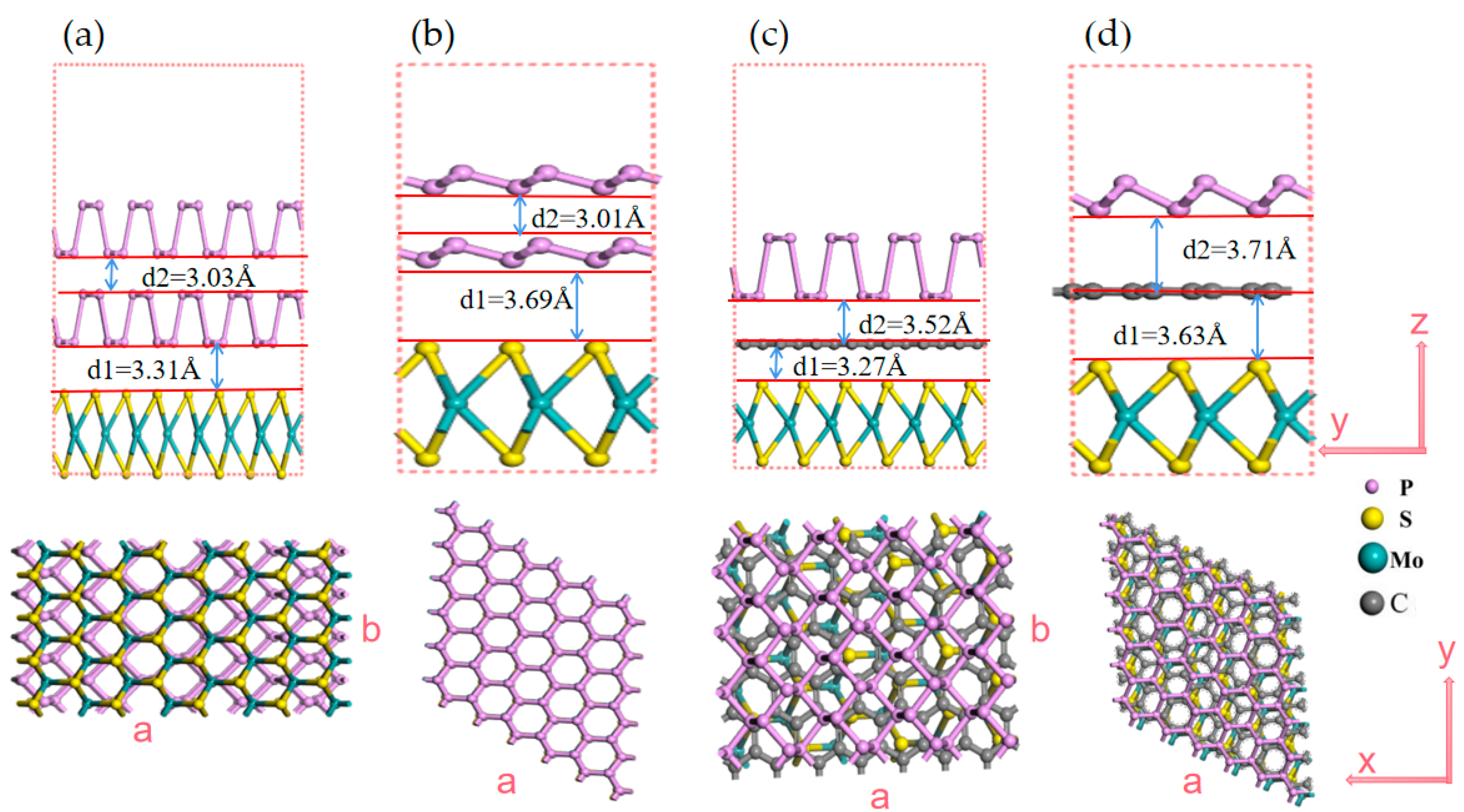
3.1. Structural Parameters

Due to the surface relaxation and interfacial mismatch, the trilayer vdW heterostructure supercells must be carefully set, for which we here extend monolayer cells individually to satisfy the length matching between different layers. The BP/BP/MoS2 heterostructure is constructed from a 4 3 × 1 supercell MoS2 monolayer and a 5 × 1 supercell bilayer-BP, while the BlueP/BlueP/MoS2 heterostructure is formed by stacking a 3 × 3 supercell bilayer-BlueP on a 3 × 3 supercell MoS2 monolayer. After structure optimization calculation, we obtain the rectangular lattice constants a = 22.227 and b = 3.278 Å for BP/BP/MoS2, and the hexagonal lattice constants a = b = 9.642 Å for BlueP/BlueP/MoS2. For BP/graphene/MoS2, bilayer BP/graphene cells are first constructed by matching 3 × 1 BP with 4 3 × 1 supercell graphene, and then the 1 × 2 supercell of the bilayer BP/graphene is set to match the 2 3 × 3 supercell MoS2. For BlueP/graphene/MoS2, a 3 × 3 supercell monolayer BlueP, 4 × 4 supercell graphene, and 3 × 3 supercell monolayer MoS2 are successively stacked. The optimized rectangular lattice constants of BP/graphene/MoS2 are a = 10.256 Å and b = 8.907 Å, and the hexagonal ones of BlueP/graphene/MoS2 are a = b = 9.776 Å. The simulated models of BP/BP/MoS2, BlueP/BlueP/MoS2, BP/graphene/MoS2 and BlueP/graphene/MoS2 are depicted in Figure 1.
The trilayer vdW heterostructures will have different energies with different layer spacing. Figure 1 gives the layer spacing when the system reaches the final equilibrium. The calculated binding energy of the four trilayer heterostructures is −21.12, −65.41, −21.92 and −65.78 eV, respectively. The negative binding energies indicate that all the four proposed vdW heterostructures are structurally highly stable like the reported bilayer heterostructures [21,36]. The structure stability may imply the fabrication feasibility to some degree. As is known, BP/MoS2 [38], graphene/MoS2 [59], graphene/BP [39] bilayer heterostructures, and TMD/graphene/MoS2 [51] trilayer heterostructures have been successfully fabricated using physical and chemical methods including mechanical stripping, liquid-phase stripping, hydrothermal and chemical vapor deposition. BlueP 2D monolayer has been well fabricated by molecular beam epitaxy [60], and the possibility to form its heterostructure with other 2D materials has been stated by a few studies [37,46]. Combining together the above fabrication abilities and considering the confirmed structure stability, the preparation of our proposed vdW heterostructures will be experimentally feasible. Noting the binding energy differences among these heterostructures, BlueP/BlueP/MoS2 and BlueP/graphene/MoS2 might be easier to be fabricated than BP/BP/MoS2 and BP/graphene/MoS2, although BlueP-related 2D materials seem currently farther away from practical manufacture than BP-related ones.

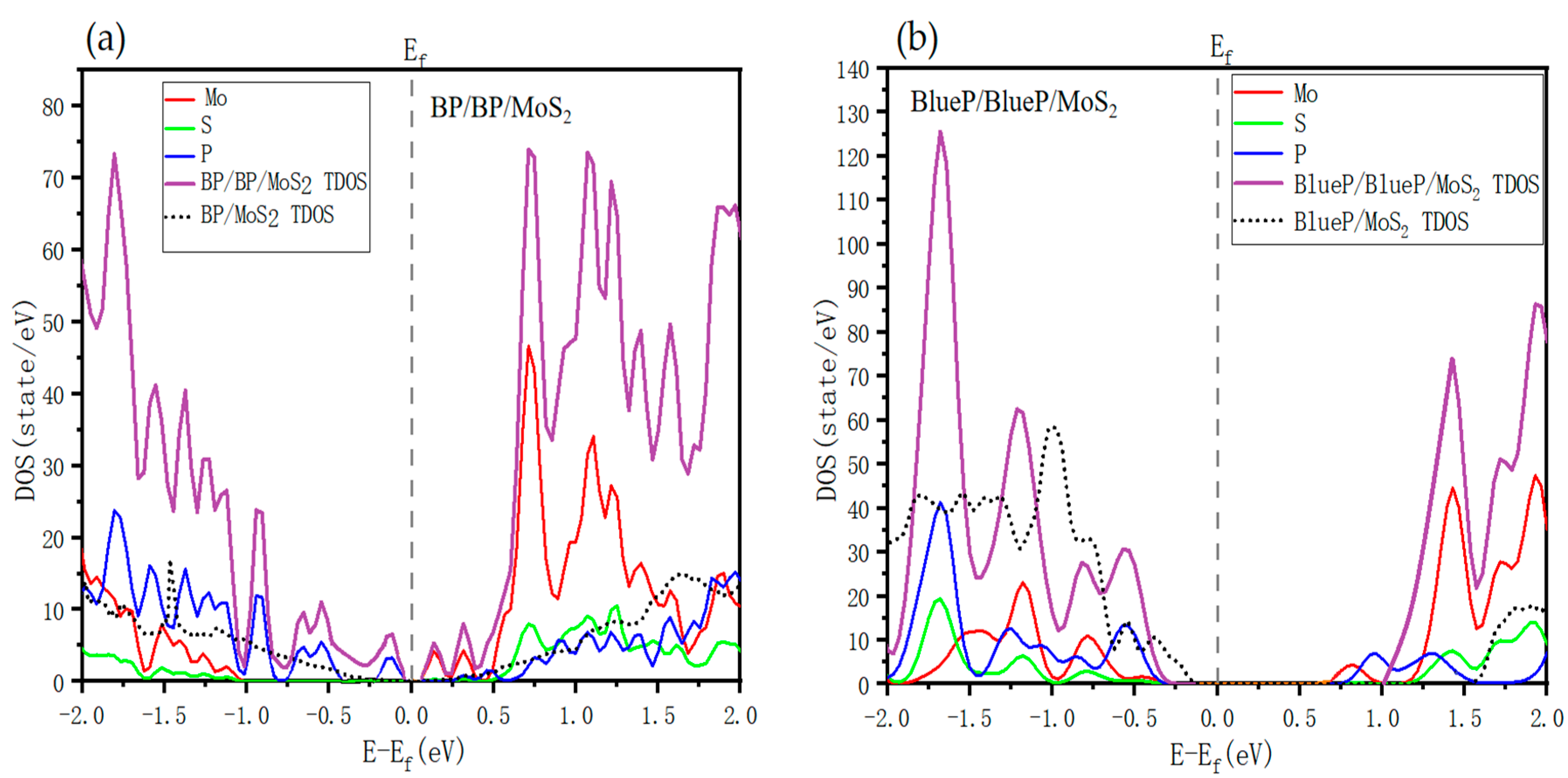
3.2. Electronic Properties

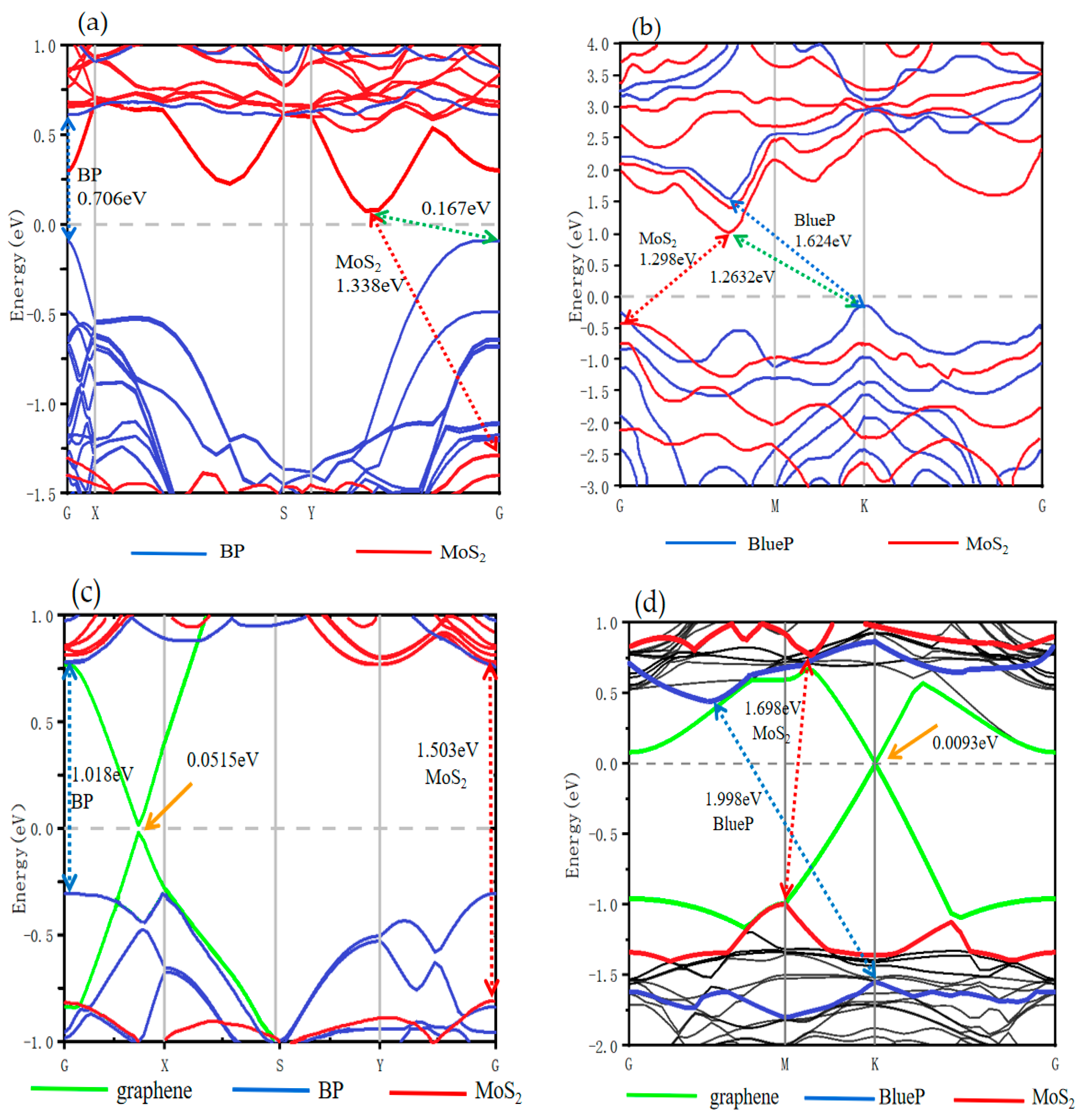
3.2.1. Band Structure

Figure 2a,b demonstrate the projected band structures of BP/BP/MoS2 and BlueP/BlueP/MoS2 calculated using the PBE method. BP/BP/MoS2 exhibits the conduction band minimum (CBM) located between the Y and G points and mostly contributed by MoS2 (red lines) as well as the valance band maximum (VBM) located at the high-symmetry G point and mostly contributed by BP (blue lines). These are qualitatively consistent with our calculation of the bilayer counterpart BP/MoS2 (in agreement with [34]), suggesting that the high hole mobility of BP and high electron mobility of MoS2 are still preserved. The indirect bandgap of the 4 3 × 1 supercell MoS2, 1.338 eV, and the direct bandgap of the 5 × 1 supercell bilayer-BP, 0.706 eV, are reduced compared with those in bilayer BP/MoS2 (MoS2 1.398 eV, BP 0.876 eV), which are already lower than the free monolayer ones (MoS2 1.69 eV, BP 0.9 eV [36]). Significantly, the whole BP/BP/MoS2 heterostructure possesses an indirect band gap of 0.167 eV, nearly half that of bilayer BP/MoS2, 0.326 eV. It is seen that this trilayer heterostructure effectively tunes the bandgap further. For BlueP/BlueP/MoS2, the CBM is located between the G and M points and is also mostly contributed by MoS2 (red lines), whereas the VBM is located at the high-symmetry K point and is mostly contributed by BlueP (blue lines), consistent with the calculated results of the bilayer counterpart BlueP/MoS2 (in agreement with [37]). Similar to the above BP/BP/MoS2, the direct bandgap of the 3 × 3 supercell MoS2 monolayer, 1.298 eV, and the indirect bandgap of the 3 × 3 supercell BlueP monolayer, 1.624 eV, are smaller than those in the bilayer BlueP/MoS2 (MoS2 1.328 eV, BlueP 1.698 eV), which are already decreased compared with the corresponding free monolayer ones (MoS2 1.69 eV, BlueP 1.908 eV [2,37]). The whole trilayer heterostructure possesses an indirect band gap of 1.2632 eV, smaller than that of the bilayer BlueP/MoS2, 1.3746 eV. It falls in between the BlueP/MoS2/BlueP of 1.013 eV and MoS2/BlueP/MoS2 of 1.561 eV reported by Han et al. [46], again implying the further effective tuning by such an asymmetric trilayer heterostructure. The BP(BlueP) and MoS2 bandgap decrease as they compose bilayer or trilayer heterostructures, which can be attributed to ~2.5% and ~2% lattice mismatch and a weak vdW force [35]. A whole-bandgap decrease with the addition of a BP(BlueP) monolayer was discovered by Dong et al. and Qiao et al. in their studies on BP [57,61]; bandgap engineering by means of the simple addition of monolayers appears thus to be effective. Moreover, it is interesting here that the VBM of BlueP and MoS2 are becoming much closer, which supports application with the function of carrier transferring or tunneling.
Figure 2c,d show the projected band structure of BP/graphene/MoS2 and BlueP/graphene/MoS2 trilayer vdW heterostructures calculated using the PBE method. What is immediately significant is that the BP/graphene/MoS2 structure opens the bandgap of graphene to 0.051 eV, which is over one order of magnitude larger than the opening by the reported bilayer heterostructures such as graphene/BP (~0.0013 eV) [24], graphene/ZnO (~0.0057 eV) [30], and graphene/MoS2 (~0.0007 eV) [49], and remarkably larger than those by other trilayer heterostructures such as graphene/ZnO/MoS2 (~0.0048 eV) [30], graphene/nitrogene/graphene (~0.04 eV) [40], and graphene/BN/graphene (~0.020 eV) [47]. BlueP/graphene/MoS2 opens the bandgap of graphene by 0.0093 eV, similar to many other heterostructures. The effectiveness of the graphene bandgap opening in BP/graphene/MoS2 can hardly be attributed to strain, because the strains of graphene in both structures are close to each other (3.2% and 2.8%) and close to those of the reported structures such as graphene/BP (3%) [24]. We believe it originates from the united vdW coupling forces among BP and MoS2 monolayers and possible built-in electric fields. The remarkable graphene bandgap opening suggests potential applications in temperature-sensitive devices [62]. On the basis of guaranteeing the excellent electronic properties of graphene, it can also be applied to field effect transistors with a high switching ratio. It is worth noting that these band gap values are grossly underestimated owing to adopting PBE functional calculation, so the real bandgaps of graphene in such heterostructures may be larger to match more extended application prospects. Furthermore, the band gap values of BP (~1.018 eV) and BlueP (~1.998 eV) in these two trilayer heterostructures are, qualitatively as graphene does, slightly larger than the free monolayers (BP of 0.9 eV [36] and BlueP of 1.908 [37]), which is in contrast to the first two structures BP/BP/MoS2 and BlueP/BlueP/MoS2. There seem to be two types of bandgap engineering mechanisms in trilayer vdW heterostructures, providing wider space for novel device design.
We also calculated the local density of state (LDOS) and total density of states (TDOS) of BP/BP/MoS2 and BlueP/BlueP/MoS2, as shown in Figure 3. The CBM state is mainly contributed by the Mo element and the VBM state relies on the P element, but the small difference between LDOS and TDOS may suggest that the interlayer vdW interaction also has a role in tuning the energy bands. What is quite significant is that only one more monolayer of BP(BlueP) increases the DOS to more than twice compared with the corresponding bilayer heterostructures. A similar phenomenon occurs in BP/graphene/MoS2 and BlueP/graphene/MoS2, where the DOS also increases due to the insertion of a single graphene monolayer with respect to BP/MoS2 and BlueP/MoS2 bilayer heterostructures. It evidences the effectiveness of the proposed trilayer vdW heterostructures in optimizing the performance of 2D material systems.

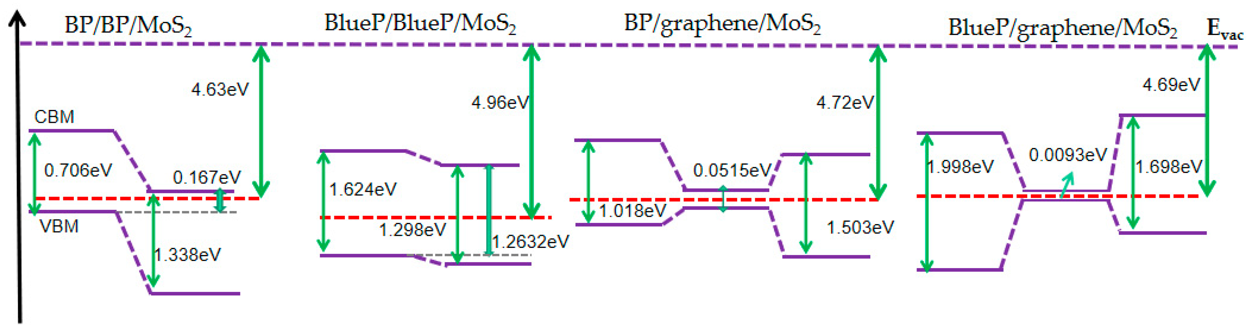
3.2.2. Band Alignment

The band alignment of the vdW heterostructure is important in the design of new 2D-material structures. It is thus necessary to specifically pick up the band alignment data from the proceeding band structures with the help of calculating the work function. In Figure 4, for the BP/BP/MoS2 and BlueP/BlueP/MoS2 heterostructures, p-type bilayer-BP(BlueP) (Efcloser to VBM) and n-type MoS2 (Ef closer to CBM) form type-II band alignment, as is expected. This band alignment has carrier confinement effects [63], favoring the electron-hole separation and then increasing the internal gain and responsivity of photodetectors. In brief, BP/BP/MoS2 shows a more obvious type-II band alignment with a larger offset on the valence band and will produce a stronger carrier confinement effect compared with BP/MoS2 [37,40]. With graphene inserted, BP/graphene/MoS2 and BlueP/graphene/MoS2 heterostructures naturally show a type-I quantum-well-like band alignment, providing the potential to construct nano-scaled bipolar transistors, field-effect transistors and photon transistors, which may need three different energy structures. In contrast to the Schottky contact of graphene/MoS2 and graphene/BP(BlueP), here, semiconductor heterojunctions are formed. By applying an electric field across this semiconductor heterojunction, the graphene bandgap can be further flexibly tuned to exhibit different band alignments, which is of significance for the construction of new types of field-effect photodetectors [49].

3.3. Optical Absorption Spectra

On the optical absorption properties of 2D materials, many studies have been devoted to monolayer and bilayer vdW heterostructures, but little research has been carried out on trilayer ones, let alone a comparison between the bilayer and trilayer heterostructures [48]. The absorption spectra of BP/BP/MoS2 and BlueP/BlueP/MoS2 trilayer heterostructures are shown in Figure 5a,b. The absorption edge redshifts effectively expand the application ranges from covering the short-wave infrared band to covering the mid-wave infrared band for BP-based material, and from covering the visible band to covering the short-wave infrared band for BlueP-based material. This change is directly associated with the shrinkage of the bandgaps observed in Figure 3, but there seems to be something more incorporated as we see the following. Obviously, with only one more phosphorene monolayer, i.e., ~1/3 increase in material quantity, the spectral absorption intensity increases to be more or less twice with respect to monolayer and bilayer counterparts. This is more than expected, meaning that these two trilayer heterostructures greatly improve the quantum efficiency in optoelectronic devices [64] in wide spectral ranges. This sort of enhancement might be the result of complex interlayer vdW interactions. In more detail, the absorption of BP/BP/MoS2 is much stronger (reaching 105 cm−1) than that of BlueP/BlueP/MoS2 in the near-infrared range, but the latter displays more significant absorption in the ultraviolet range. They can thus be applied effectively in different scenes. As a whole, these results make up for the shortage of monolayer 2D materials in optical characteristics and are beneficial for optoelectronic devices with the need for light absorption enhancement and absorption range broadening.
Figure 6 displays the absorption coefficients of bilayer heterostructures graphene/BP, graphene/BlueP and graphene/MoS2, and the trilayer heterostructures BP/graphene/MoS2 and BlueP/graphene/MoS2. The inset shows that the two kinds of trilayer heterostructures have stronger light absorption in the range below 0.8 eV than the related bilayer heterostructures, so they are better choices for graphene-based 2D materials to realize photodetectors widely responding to short-, mid- and long-wave infrared light. In the range of 2.2–6 eV, BP/graphene/MoS2 shows remarkably higher light absorption than the related bilayer heterostructures, making it able to realize better graphene-based optoelectronic devices working in a wide range from visible to deep ultraviolet. BlueP/graphene/MoS2 shows better light absorption characteristics than the related bilayer heterostructures in the range of 4–6 eV, so it is more suitable for use as a graphene-based solar-blind ultraviolet photodetector. These asymmetric graphene-sandwiched vdW heterostructrues are thus proved to be effective in tuning and improving the performance of graphene-based 2D materials on the basis of guaranteeing the excellent electronic properties of graphene.

4. Conclusions

Using the first-principles calculation based on DFT theory, we proposed and simulated trilayer 2D vdW heterostructures: BP/BP/MoS2, BlueP/BlueP/MoS2, BP/graphene/MoS2 and BlueP/graphene/MoS2. The atomic structures of these heterostructures are all stable and look feasible to prepare. For BP/BP/MoS2 and BlueP/BlueP/MoS2, all the bandgaps were tuned to be smaller, to effectively compensate for the shortage of corresponding monolayers and to satisfy a wider spectrum of applications with respect to the bilayer structures BP/MoS2 and BlueP/MoS2, respectively. Their higher DOS, much stronger light absorption and more obvious type-II band alignment will realize better performance of optoelectronic devices working in a wide spectrum from mid-wave (short-wave) infrared to violet. In contrast, for BP/graphene/MoS2 and BlueP/graphene/MoS2, most of the bandgaps were enlarged, implying different tuning mechanisms related to vdW interaction. Specifically in BP/graphene/MoS2, the graphene bandgap was well opened to 0.051 eV, more than one order of magnitude larger than usual, indicating more space for graphene tuning in trilayer vdW heterostructures. Accompanying the bandgap increase, both BP/graphene/MoS2 and BlueP/graphene/MoS2 exhibit absorption enhancement in wide spectral ranges, suggesting that these trilayer vdW heterostructures show better prospects as graphene-based 2D material optoelectronic devices with broad responses in the short- to long-wave infrared, visible to deep ultraviolet and solar-blind ultraviolet bands. It is concluded that the proposed 2D trilayer vdW heterostructures are potentially applicable as novel optoelectronic devices.

Author Contributions

B.C.: model building, simulation, data processing, and writing—original draft; Y.Z., R.J., X.W., S.H., X.H., W.Z., Q.D. and L.Z.: investigation help and discussion; P.L.: simulation instruction, discussion and revision guidance; H.-Z.S.: writing and revision guidance, project administration, resources, and supervision. All authors have read and agreed to the published version of the manuscript.

Funding

This research was supported by the National Key Research and Development Program of China under grants No. 2019YFB2203400 and No. 2021YFA0718803, and by the Natural Science Foundation of Sichuan Province under grant No. 2022NSFSC1817. We also acknowledge the support of the Special Subject of Significant Science and Technology of Sichuan Province under grant 2018TZDZX0001 and the Special Subject of Significant Innovation of Chengdu City under grant 2021-YF08-00159-GX.

Data Availability Statement

The data presented in this study are available on request from the corresponding author.

Conflicts of Interest

The authors declare no conflict of interest.

References

  1. Miao, J.; Wang, C. Avalanche photodetectors based on two-dimensional layered materials. Nano Res. 2021, 14, 1878–1888. [Google Scholar] [CrossRef]
  2. Liu, Y.; Weiss, N.O.; Duan, X.; Cheng, H.C.; Huang, Y.; Duan, X. Van der Waals heterostructures and devices. Nat. Rev. Mater. 2016, 1, 16042. [Google Scholar] [CrossRef]
  3. Das, S.; Gulotty, R.; Sumant, A.V.; Roelofs, A. All two-dimensional, flexible, transparent, and thinnest thin film transistor. Nano Lett. 2014, 14, 2861–2866. [Google Scholar] [CrossRef] [PubMed]
  4. Long, M.; Wang, P.; Fang, H.; Hu, W. Progress, challenges, and opportunities for 2D material based photodetectors. Adv. Funct. Mater. 2019, 29, 1803807. [Google Scholar] [CrossRef]
  5. Akinwande, D.; Huyghebaert, C.; Wang, C.H.; Serna, M.I.; Goossens, S.; Li, L.J.; Koppens, F.H. Graphene and two-dimensional materials for silicon technology. Nature 2019, 573, 507–518. [Google Scholar] [CrossRef] [PubMed]
  6. Geim, A.K.; Grigorieva, I.V. Van der Waals heterostructures. Nature 2013, 499, 419–425. [Google Scholar] [CrossRef]
  7. Novoselov, K.S.; Mishchenko, O.A.; Carvalho, O.A.; Castro Neto, A.H. 2D materials and van der Waals heterostructures. Science 2016, 353, aac9439. [Google Scholar] [CrossRef]
  8. Jariwala, D.; Marks, T.J.; Hersam, M.C. Mixed-dimensional van der Waals heterostructures. Nat. Mater. 2017, 16, 170–181. [Google Scholar] [CrossRef]
  9. Wang, H.; Li, Z.; Li, D.; Chen, P.; Pi, L.; Zhou, X.; Zhai, T. Van der Waals Integration Based on Two-Dimensional Materials for High-Performance Infrared Photodetectors. Adv. Funct. Mater. 2021, 31, 2103106. [Google Scholar] [CrossRef]
  10. Wang, P.; Xia, H.; Li, Q.; Wang, F.; Zhang, L.; Li, T.; Hu, W. Sensing infrared photons at room temperature: From bulk materials to atomic layers. Small 2019, 15, 1904396. [Google Scholar] [CrossRef]
  11. Guan, X.; Yu, X.; Periyanagounder, D.; Benzigar, M.R.; Huang, J.K.; Lin, C.H.; Wu, T. Recent progress in short-to long-wave infrared photodetection using 2D materials and heterostructures. Adv. Opt. Mater. 2021, 9, 2001708. [Google Scholar] [CrossRef]
  12. Rogalski, A.; Antoszewski, J.; Faraone, L. Third-generation infrared photodetector arrays. J. Appl. Phys. 2009, 105, 344–348. [Google Scholar] [CrossRef]
  13. Rhodes, D.; Chae, S.H.; Ribeiro-Palau, R.; Hone, J. Disorder in van der Waals heterostructures of 2D materials. Nat. Mater. 2019, 18, 541–549. [Google Scholar] [CrossRef] [PubMed]
  14. Geim, A.K.; Novoselov, K.S. The rise of graphene. Nat. Mater. 2007, 6, 183–191. [Google Scholar] [CrossRef]
  15. Bhimanapati, G.R.; Lin, Z.; Meunier, V.; Jung, Y.; Cha, J.; Das, S.; Robinson, J.A. Recent advances in two-dimensional materials beyond graphene. ACS Nano 2015, 9, 11509–11539. [Google Scholar] [CrossRef]
  16. Ebnonnasir, A.; Narayanan, B.; Kodambaka, S.; Ciobanu, C.V. Tunable MoS2 bandgap in MoS2-graphene heterostructures. Appl. Phys. Lett. 2014, 105, 031603. [Google Scholar] [CrossRef]
  17. Radisavljevic, B.; Radenovic, A.; Brivio, J.; Giacometti, V.; Kis, A. Single-layer MoS2 transistors. Nat. Nanotechnol. 2011, 6, 147–150. [Google Scholar] [CrossRef]
  18. Zong, X.; Hu, H.; Ouyang, G.; Wang, J.; Shi, R.; Zhang, L.; Chen, X. Black phosphorus-based van der Waals heterostructures for mid-infrared light-emission applications. Light Sci. Appl. 2020, 9, 114. [Google Scholar] [CrossRef]
  19. Chen, P.; Li, N.; Chen, X.; Ong, W.J.; Zhao, X. The rising star of 2D black phosphorus beyond graphene: Synthesis, properties and electronic applications. 2d Mater. 2017, 5, 014002. [Google Scholar] [CrossRef]
  20. Castellanos-Gomez, A. Black phosphorus: Narrow gap, wide applications. J. Phys. Chem. Lett. 2015, 6, 4280–4291. [Google Scholar] [CrossRef]
  21. Zhao, X.; Bo, M.; Huang, Z.; Zhou, J.; Peng, C.; Li, L. Heterojunction bond relaxation and electronic reconfiguration of WS2-and MoS2-based 2D materials using BOLS and DFT. Appl. Surf. Sci. 2018, 462, 508–516. [Google Scholar] [CrossRef]
  22. Hu, W.; Wang, T.; Zhang, R.; Yang, J. Effects of interlayer coupling and electric fields on the electronic structures of graphene and MoS2 heterobilayers. J. Mater. Chem. C 2016, 4, 1776–1781. [Google Scholar] [CrossRef]
  23. Le, N.B.; Huan, T.D.; Woods, L.M. Interlayer interactions in van der Waals heterostructures: Electron and phonon properties. ACS Appl. Mater. Interfaces 2016, 8, 6286–6292. [Google Scholar] [CrossRef] [PubMed]
  24. Cai, Y.; Zhang, G.; Zhang, Y.W. Electronic properties of phosphorene/graphene and phosphorene/hexagonal boron nitride heterostructures. J. Phys. Chem. C 2015, 119, 13929–13936. [Google Scholar] [CrossRef]
  25. Su, J.; Xiao, B.; Jia, Z. A first principle study of black phosphorene/N-doped graphene heterostructure: Electronic, mechanical and interface properties. Appl. Surf. Sci. 2020, 528, 146962. [Google Scholar] [CrossRef]
  26. Behera, S.K.; Deb, P. Controlling the bandgap in graphene/h-BN heterostructures to realize electron mobility for high performing FETs. RSC Adv. 2017, 7, 31393–31400. [Google Scholar] [CrossRef]
  27. Komsa, H.P.; Krasheninnikov, A.V. Electronic structures and optical properties of realistic transition metal dichalcogenide heterostructures from first principles. Phys. Rev. B 2013, 88, 085318. [Google Scholar] [CrossRef]
  28. Lu, N.; Guo, H.; Li, L.; Dai, J.; Wang, L.; Mei, W.N.; Zeng, X.C. MoS2/MX2 heterobilayers: Bandgap engineering via tensile strain or external electrical field. Nanoscale 2014, 6, 2879–2886. [Google Scholar] [CrossRef]
  29. Ren, K.; Sun, M.; Luo, Y.; Wang, S.; Yu, J.; Tang, W. First-principle study of electronic and optical properties of two-dimensional materials-based heterostructures based on transition metal dichalcogenides and boron phosphide. Appl. Surf. Sci. 2019, 476, 70–75. [Google Scholar] [CrossRef]
  30. Wang, S.; Tian, H.; Ren, C.; Yu, J.; Sun, M. Electronic and optical properties of heterostructures based on transition metal dichalcogenides and graphene-like zinc oxide. Sci. Rep. 2018, 8, 12009. [Google Scholar] [CrossRef]
  31. Huang, L.; Li, J. Tunable electronic structure of black phosphorus/blue phosphorus van der Waals pn heterostructure. Appl. Phys. Lett. 2016, 108, 083101. [Google Scholar] [CrossRef]
  32. Sun, M.; Chou, J.-P.; Yu, J.; Tang, W. Electronic properties of blue phosphorene/graphene and blue phosphorene/graphene-like gallium nitride heterostructures. Phys. Chem. Chem. Phys. 2017, 19, 17324–17330. [Google Scholar] [CrossRef] [PubMed]
  33. Liao, C.; Zhao, Y.; Ouyang, G. Strain-modulated band engineering in two-dimensional black phosphorus/MoS2 van der Waals heterojunction. ACS Omega 2018, 3, 14641–14649. [Google Scholar] [CrossRef] [PubMed]
  34. Huang, L.; Huo, N.; Li, Y.; Chen, H.; Yang, J.; Wei, Z.; Li, S.S. Electric-field tunable band offsets in black phosphorus and MoS2 van der Waals pn heterostructure. J. Phys. Chem. Lett. 2015, 6, 2483–2488. [Google Scholar] [CrossRef] [PubMed]
  35. Tang, K.; Qi, W.; Li, Y.; Wang, T. Electronic properties of van der Waals heterostructure of black phosphorus and MoS2. J. Phys. Chem. C 2018, 122, 7027–7032. [Google Scholar] [CrossRef]
  36. You, B.; Wang, X.; Zheng, Z.; Mi, W. Black phosphorene/monolayer transition-metal dichalcogenides as two dimensional van der Waals heterostructures: A first-principles study. Phys. Chem. Chem. Phys. 2016, 18, 7381–7388. [Google Scholar] [CrossRef]
  37. Yang, F.; Han, J.; Zhang, L.; Tang, X.; Zhuo, Z.; Tao, Y.; Dai, Y. Adjustable electronic and optical properties of BlueP/MoS2 van der Waals heterostructure by external strain: A First-principles study. Nanotechnology 2020, 31, 375706. [Google Scholar] [CrossRef]
  38. Ye, L.; Li, H.; Chen, Z.; Xu, J. Near-infrared photodetector based on MoS2/black phosphorus heterojunction. ACS Photonics 2016, 3, 692–699. [Google Scholar] [CrossRef]
  39. Liu, Y.; Shivananju, B.N.; Wang, Y.; Zhang, Y.; Yu, W.; Xiao, S.; Bao, Q. Highly efficient and air-stable infrared photodetector based on 2D layered graphene–black phosphorus heterostructure. ACS Appl. Mater. Interfaces 2017, 9, 36137–36145. [Google Scholar] [CrossRef]
  40. Li, R. Electronic properties of hybrid graphene/nitrogene/graphene hetero-trilayers. Phys. E Low-Dimens. Syst. Nanostructures 2020, 123, 114166. [Google Scholar] [CrossRef]
  41. Liu, B.; Chen, Y.; You, C.; Liu, Y.; Kong, X.; Li, J.; Zhang, Y. High performance photodetector based on graphene/MoS2/graphene lateral heterostrurcture with Schottky junctions. J. Alloys Compd. 2019, 779, 140–146. [Google Scholar] [CrossRef]
  42. Datta, K.; Khosru, Q.D. Electronic properties of MoS2/MX2/MoS2 trilayer heterostructures: A first principle study. ECS J. Solid State Sci. Technol. 2016, 5, Q3001–Q3007. [Google Scholar] [CrossRef]
  43. Datta, K.; Shadman, A.; Rahman, E.; Khosru, Q.D.M. Trilayer TMDC Heterostructures for MOSFETs and Nanobiosensors. J. Electron. Mater. 2017, 46, 1248–1260. [Google Scholar] [CrossRef]
  44. Bafekry, A.; Yagmurcukardes, M.; Akgenc, B.; Ghergherehchi, M.; Nguyen, C.V. Van der Waals heterostructures of MoS2 and Janus MoSSe monolayers on graphitic boron-carbon-nitride (BC3, C3N, C3N4 and C4N3) nanosheets: A first-principles study. J. Phys. D: Appl. Phys. 2020, 53, 355106. [Google Scholar] [CrossRef]
  45. Liu, S.; Li, X.; Meng, D.; Li, S.; Chen, X.; Hu, T. Tunable electronic properties of MoS2/SiC heterostructures: A First-Principles study. J. Electron. Mater. 2022, 51, 3714–3726. [Google Scholar] [CrossRef]
  46. Han, J.; Yang, F.; Xu, L.; Zhuo, Z.; Cao, X.; Tao, Y.; Liu, W. Modulated electronic and optical properties of bilayer/trilayer Blue Phosphorene/MoX2 (X= S, Se) van der Waals heterostructures. Surf. Interfaces 2021, 25, 101228. [Google Scholar] [CrossRef]
  47. Kim, D.; Hashmi, A.; Hwang, C.; Hong, J. Thickness dependent band gap and effective mass of BN/graphene/BN and graphene/BN/graphene heterostructures. Surf. Sci. 2013, 610, 27–32. [Google Scholar] [CrossRef]
  48. Farooq, M.U.; Hashmi, A.; Hong, J. Thickness dependent optical properties of multilayer BN/graphene/BN. Surf. Sci. 2015, 634, 25–30. [Google Scholar] [CrossRef]
  49. Xu, L.; Huang, W.Q.; Hu, W.; Yang, K.; Zhou, B.X.; Pan, A.; Huang, G.F. Two-dimensional MoS2-graphene-based multilayer van der Waals heterostructures: Enhanced charge transfer and optical absorption, and electric-field tunable Dirac point and band gap. Chem. Mater. 2017, 29, 5504–5512. [Google Scholar] [CrossRef]
  50. Xia, C.; Du, J.; Fang, L.; Li, X.; Zhao, X.; Song, X.; Wang, T.; Li, J. PtSe2/graphene hetero-multilayer: Gate-tunable Schottky barrier height and contact type. Nanotechnology 2018, 29, 465707. [Google Scholar] [CrossRef]
  51. Long, M.; Liu, E.; Wang, P.; Gao, A.; Xia, H.; Luo, W.; Miao, F. Broadband photovoltaic detectors based on an atomically thin heterostructure. Nano Lett. 2016, 16, 2254–2259. [Google Scholar] [CrossRef] [PubMed]
  52. Li, A.; Chen, Q.; Wang, P.; Gan, Y.; Qi, T.; Wang, P.; Gong, Y. Ultrahigh-sensitive broadband photodetectors based on dielectric shielded MoTe2/Graphene/SnS2 p–g–n junctions. Adv. Mater. 2019, 31, 1805656. [Google Scholar] [CrossRef] [PubMed]
  53. Sun, G.; Kürti, J.; Rajczy, P.; Kertesz, M.; Hafner, J.; Kresse, G. Performance of the Vienna ab initio simulation package (VASP) in chemical applications. J. Mol. Struct. THEOCHEM 2003, 624, 37–45. [Google Scholar] [CrossRef]
  54. Hafner, J. Ab-initio simulations of materials using VASP: Density-functional theory and beyond. J. Comput. Chem. 2008, 29, 2044–2078. [Google Scholar] [CrossRef] [PubMed]
  55. Bucko, T.; Hafner, J.; Lebegue, S.; Angyan, J.G. Improved description of the structure of molecular and layered crystals: Ab initio DFT calculations with van der Waals corrections. J. Phys. Chem. A 2010, 114, 11814–11824. [Google Scholar] [CrossRef]
  56. Klimeš, J.; Bowler, D.R.; Michaelides, A. Chemical accuracy for the van der Waals density functional. J. Phys. Condens. Matter 2010, 22, 022201. [Google Scholar] [CrossRef]
  57. Dong, H.M.; Huang, L.S.; Liu, J.L.; Huang, F.; Zhao, C.X. Layer-dependent optoelectronic properties of black phosphorus. Int. J. Mod. Phys. C 2020, 31, 2050177. [Google Scholar] [CrossRef]
  58. Sun, M.; Chou, J.P.; Gao, J.; Cheng, Y.; Hu, A.; Tang, W.; Zhang, G. Exceptional optical absorption of buckled arsenene covering a broad spectral range by molecular doping. ACS Omega 2018, 3, 8514–8520. [Google Scholar] [CrossRef]
  59. Yu, L.; Lee, Y.H.; Ling, X.; Santos, E.J.; Shin, Y.C.; Lin, Y.; Palacios, T. Graphene/MoS2 hybrid technology for large-scale two-dimensional electronics. Nano Lett. 2014, 14, 3055–3063. [Google Scholar] [CrossRef]
  60. Zhang, J.L.; Zhao, S.; Han, C.; Wang, Z.; Zhong, S.; Sun, S.; Guo, R.; Zhou, X.; Gu, C.D.; Yuan, K.D.; et al. Epitaxial growth of single layer blue phosphorus: A new phase of two-dimensional phosphorus. Nano Lett. 2016, 16, 4903–4908. [Google Scholar] [CrossRef]
  61. Qiao, J.; Kong, X.; Hu, Z.X.; Yang, F.; Ji, W. High-mobility transport anisotropy and linear dichroism in few-layer black phosphorus. Nat. Commun. 2014, 5, 4475. [Google Scholar] [CrossRef] [PubMed]
  62. Yan, J.; Kim, M.H.; Elle, J.A.; Sushkov, A.B.; Jenkins, G.S.; Milchberg, H.M.; Fuhrer, M.S.; Drew, H.D. Dual-gated bilayer graphene hot-electron bolometer. Nat. Nanotechnol. 2012, 7, 472–478. [Google Scholar] [CrossRef] [PubMed]
  63. Kim, J.D.; Chen, X.; Li, X.; Coleman, J.J. Photocurrent density enhancement of a III-V inverse quantum dot intermediate band gap photovoltaic device. In Proceedings of the 2015 Conference on Lasers and Electro-Optics (CLEO), San Jose, CA, USA, 10–15 May 2015. [Google Scholar]
  64. Joseph, I.; Wan, K.; Hussain, S.; Guo, L.; Xie, L.; Shi, X. Interlayer angle-dependent electronic structure and optoelectronic properties of BP-MoS2 heterostructure: A first principle study. Comput. Mater. Sci. 2021, 186, 110056. [Google Scholar] [CrossRef]
Figure 1. The models of trilayer 2D vdW heterostructures. (a) BP/BP/MoS2; (b) BlueP/BlueP/MoS2; (c) BP/graphene/MoS2; (d) BlueP/graphene/MoS2.
Nanomaterials 13 01574 g001
Figure 2. Calculated projected band structures for trilayer vdW heterostructures (a) BP/BP/MoS2; (b) BlueP/BlueP/MoS2; (c) BP/graphene/MoS2; (d) BlueP/graphene/MoS2. The Fermi level Ef is set as zero energy.
Nanomaterials 13 01574 g002
Figure 3. Calculated LDOS and TDOS for (a) BP/BP/MoS2 and (b) BlueP/BlueP/MoS2. The different colors represent different elements. The gray dashed line indicates Fermi energy. That of bilayer counterpart is also shown for comparison.
Nanomaterials 13 01574 g003
Figure 4. Band alignments of BP/BP/MoS2, BlueP/BlueP/MoS2, BP/graphene/MoS2 and BlueP/graphene/MoS2. The red dashed lines represent the Fermi levels. The vacuum level (Evac) is shown by a purple dashed line.
Nanomaterials 13 01574 g004
Figure 5. Optical absorption coefficient of (a) monolayer BP and MoS2, bilayer BP, BP/MoS2 and BP/BP/MoS2; and (b) monolayer BlueP and MoS2, bilayer BlueP, BP/MoS2 and BlueP/BlueP/MoS2.
Nanomaterials 13 01574 g005
Figure 6. Optical absorption coefficient of BP/graphene/MoS2 and BlueP/graphene/MoS2 heterostructures, and the optical absorption coefficient of graphene/BP, graphene/BlueP and graphene/MoS2 are also shown for comparison.
Nanomaterials 13 01574 g006
Disclaimer/Publisher’s Note: The statements, opinions and data contained in all publications are solely those of the individual author(s) and contributor(s) and not of MDPI and/or the editor(s). MDPI and/or the editor(s) disclaim responsibility for any injury to people or property resulting from any ideas, methods, instructions or products referred to in the content.

