
Semiconductor-to-Insulator Transition in Inter-Electrode Bridge-like Ensembles of Anatase Nanoparticles under a Long-Term Action of the Direct Current

 , , ,
, , ,  ,
,  , ,
, , 
Abstract
:1. Introduction
2. Materials and Methods
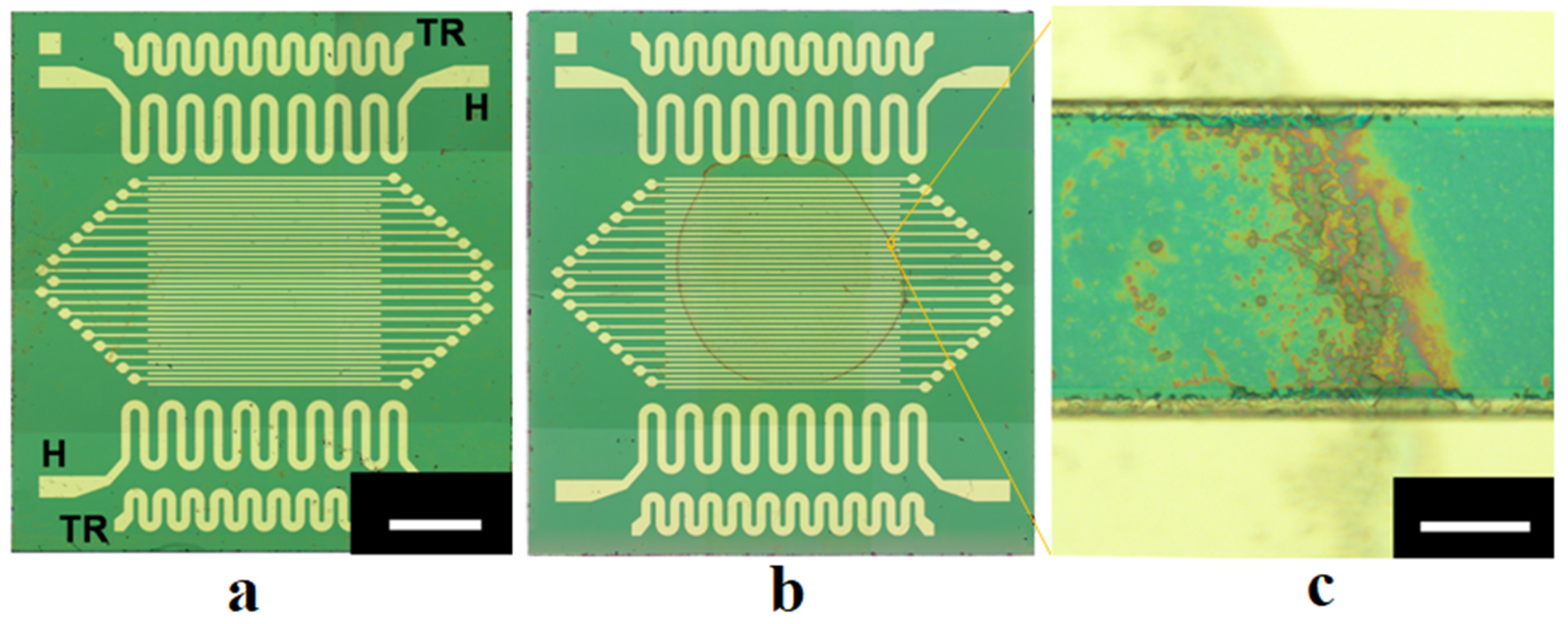
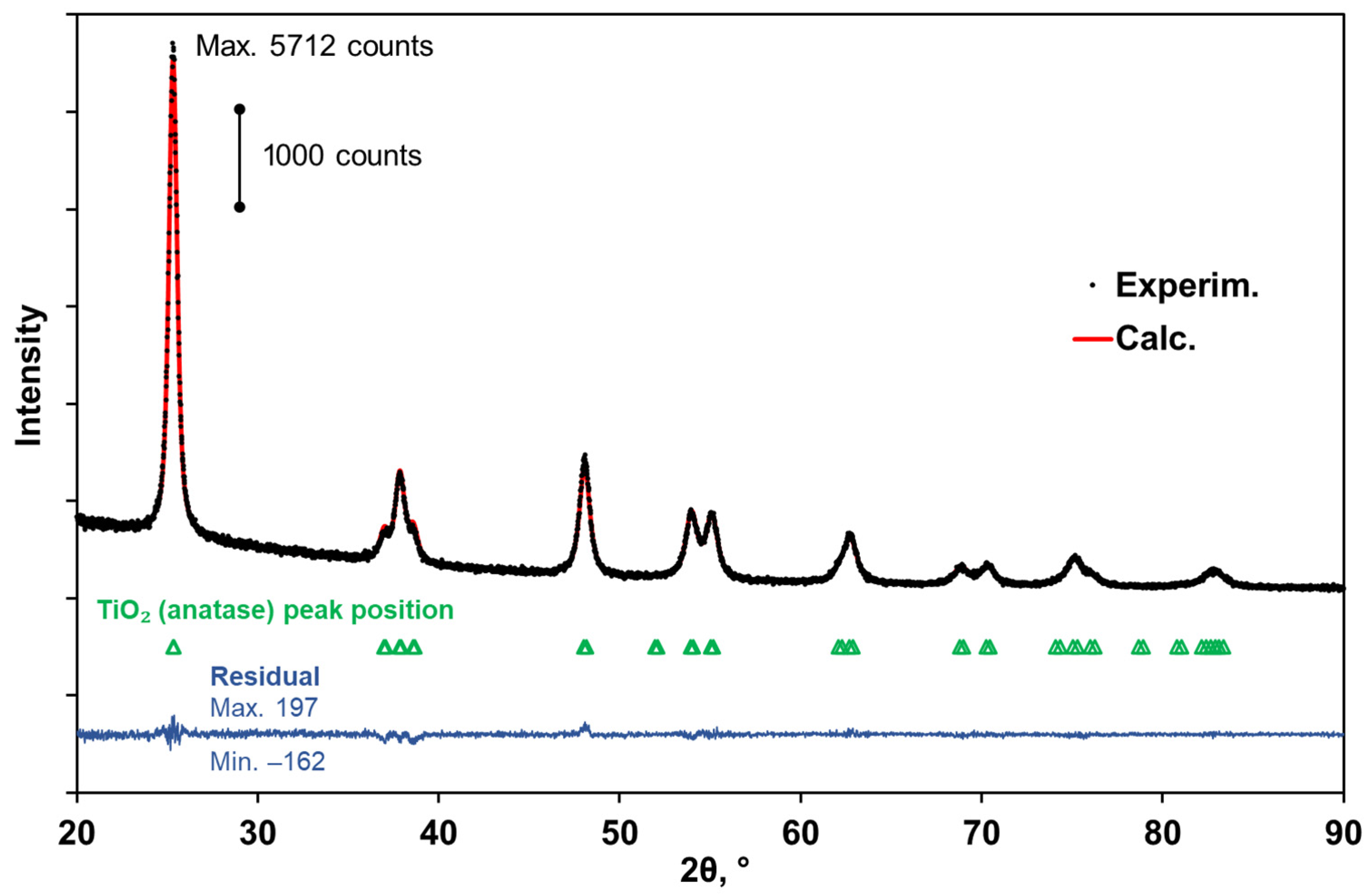
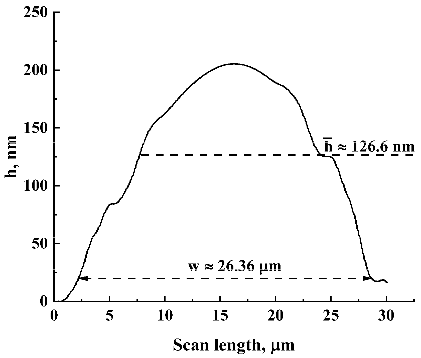
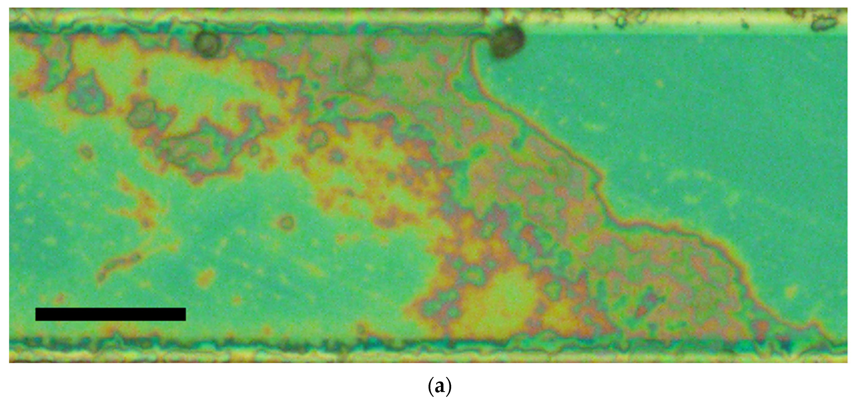
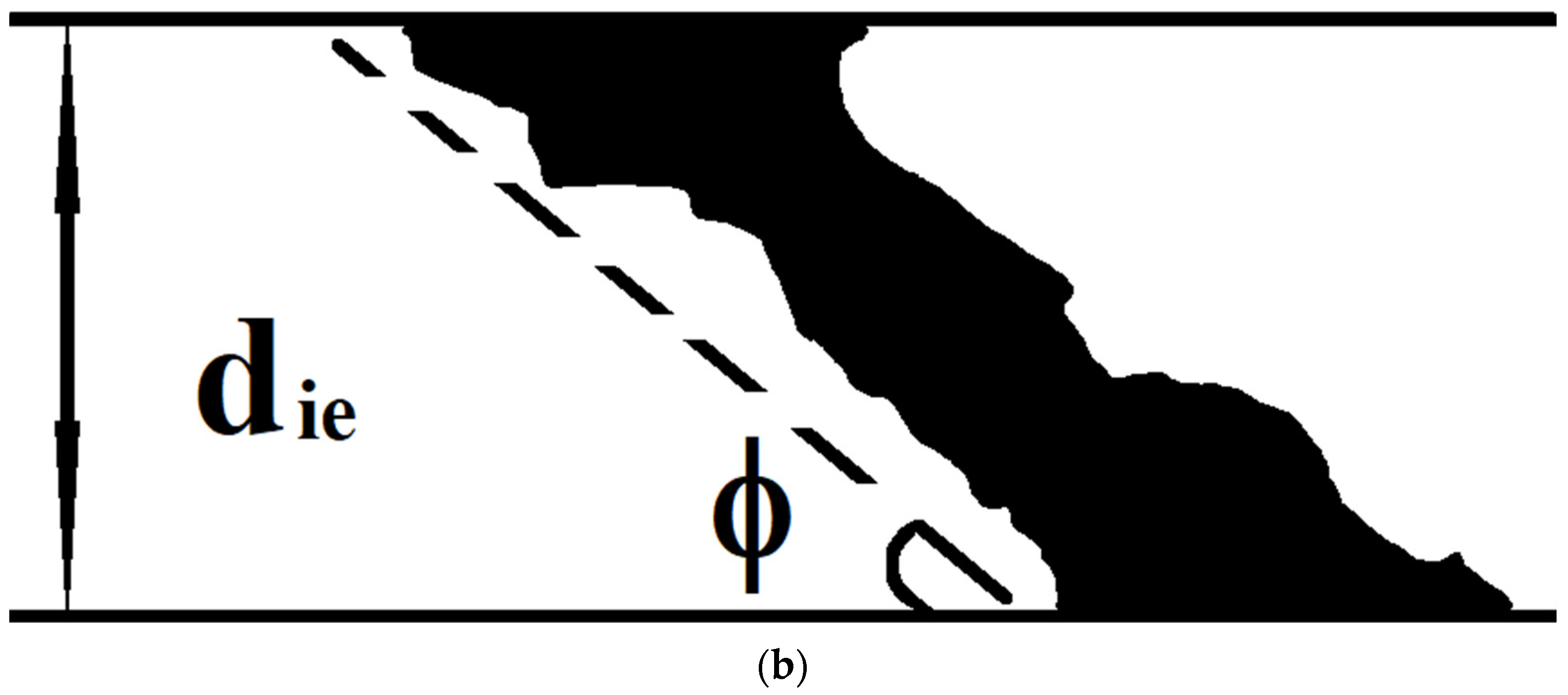
2.1. Sample Preparation and Characterization
- (1)
- with an inter-electrode distance of (103.8 ± 3.9) μm and electrode width of (89.8 ± 5.7) μm;
- (2)
- with the inter-electrode distance of (44.9 ± 4.0) μm and electrode width of (54.2 ± 5.2) μm.
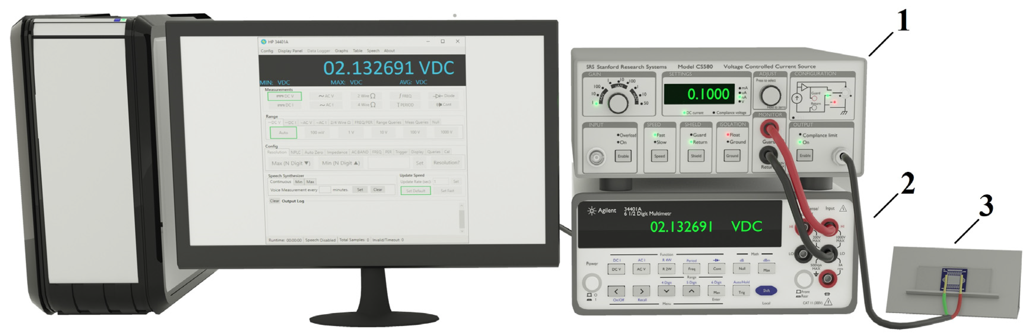
2.2. Sample Examination
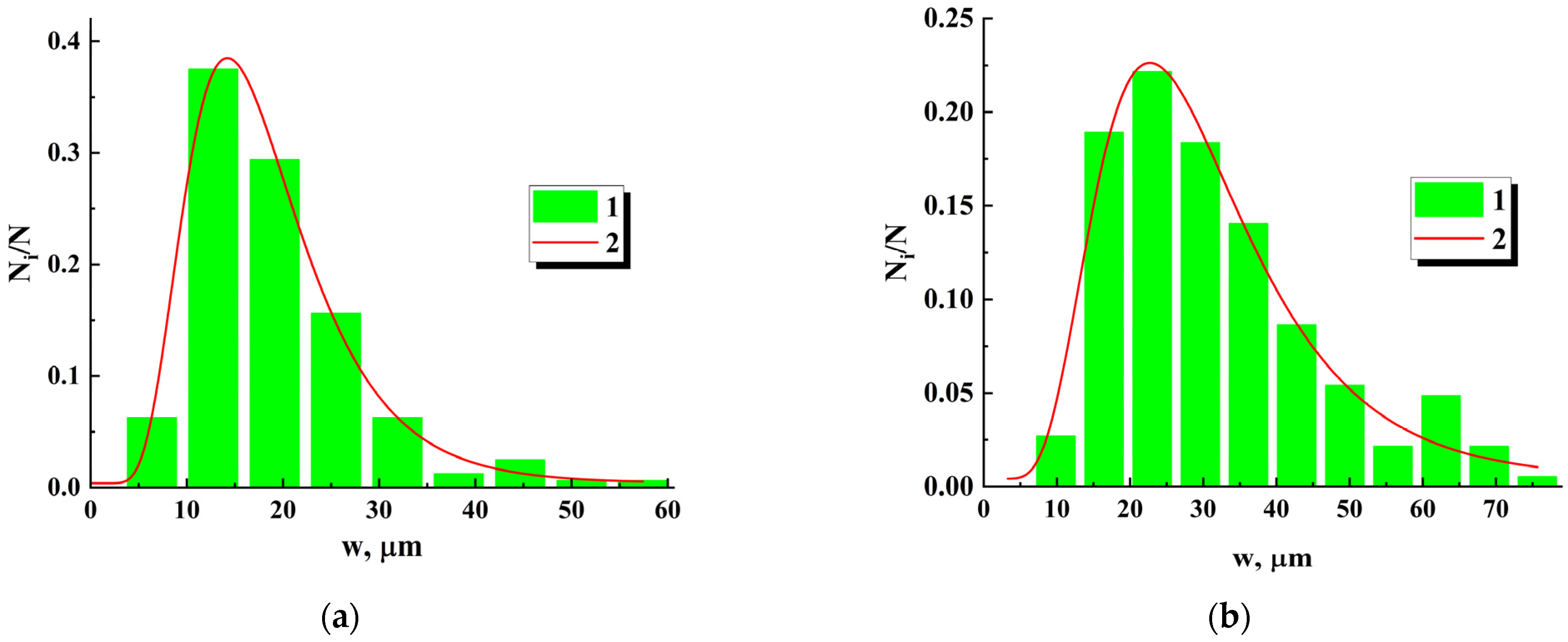
3. Results
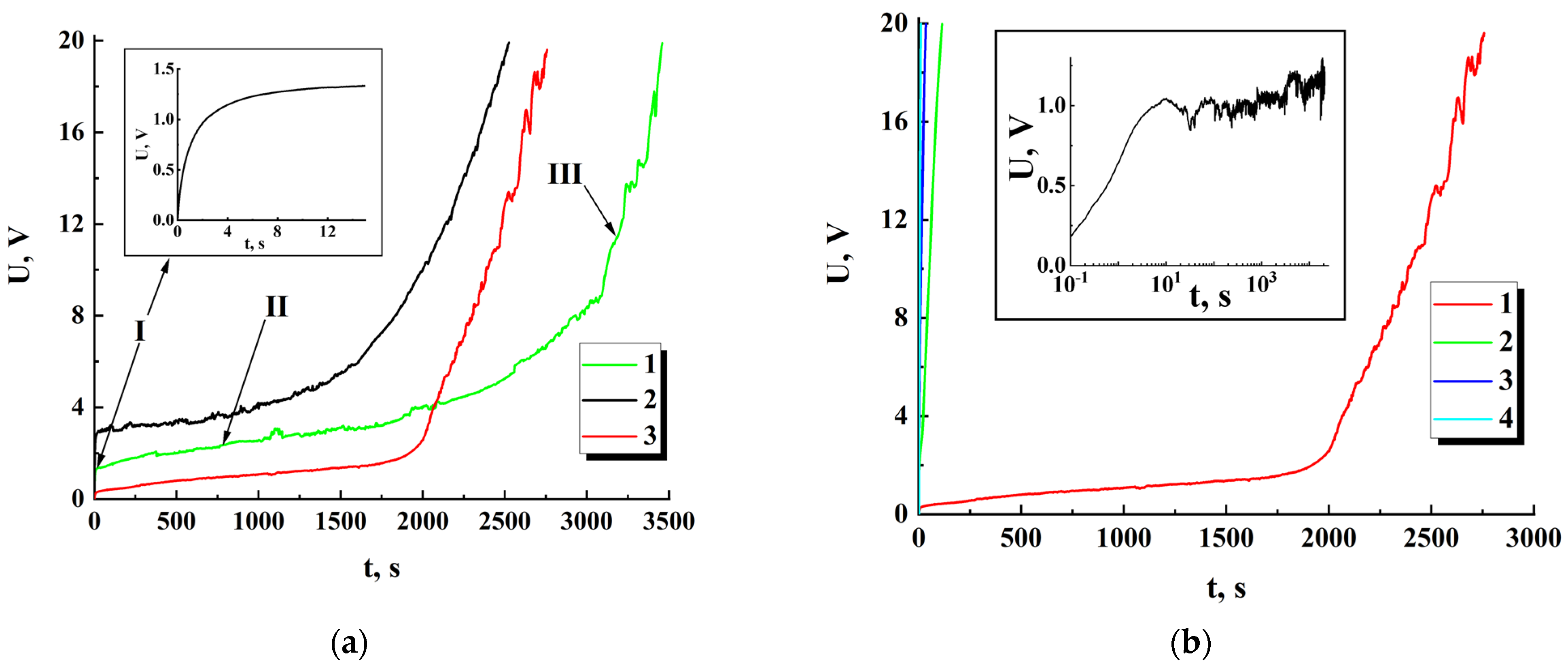
4. Discussion
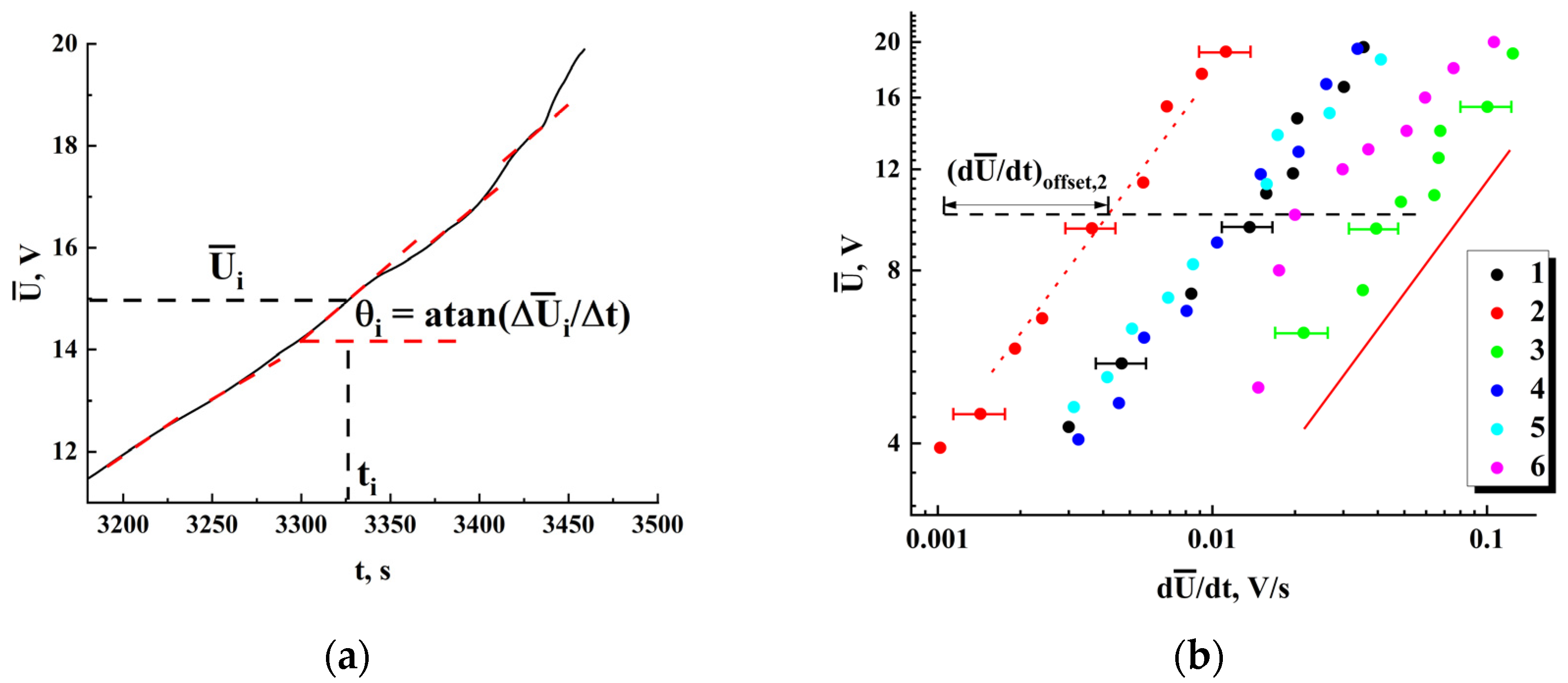
4.1. Recovery of Time-Dependent Smoothed Conductivity in the Examined Samples
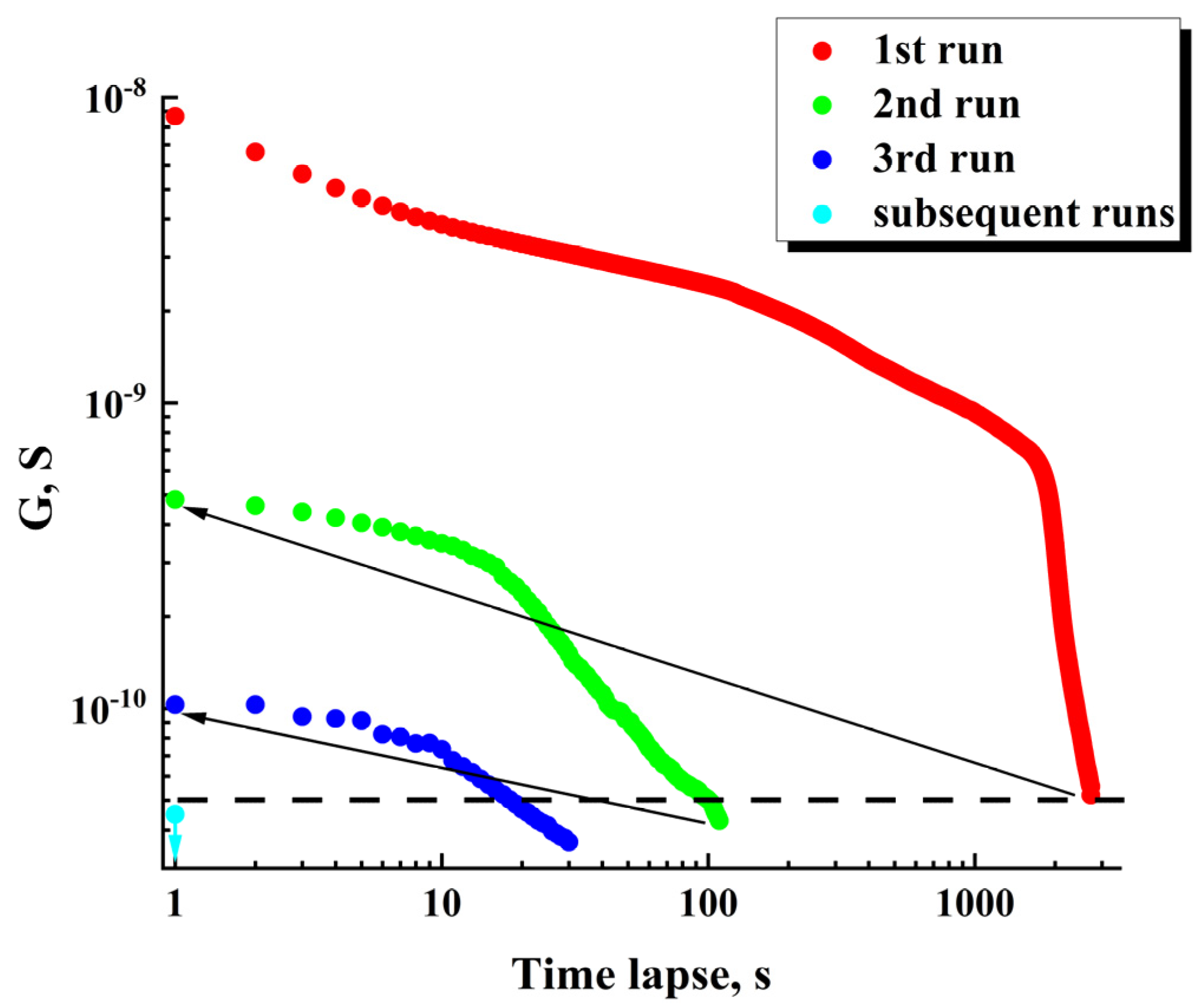
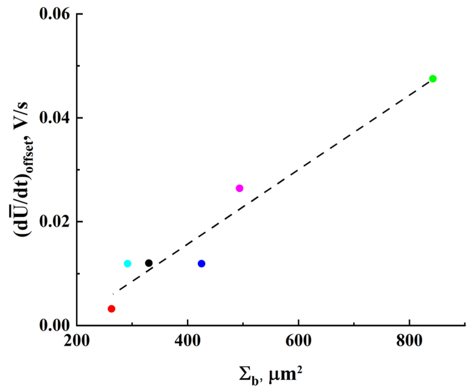
4.2. Scaling Behavior of and the Conductivity Critical Exponent
4.3. Comments on DC Conductivity and Permittivity of the Studied Systems
- (1)
- (2)
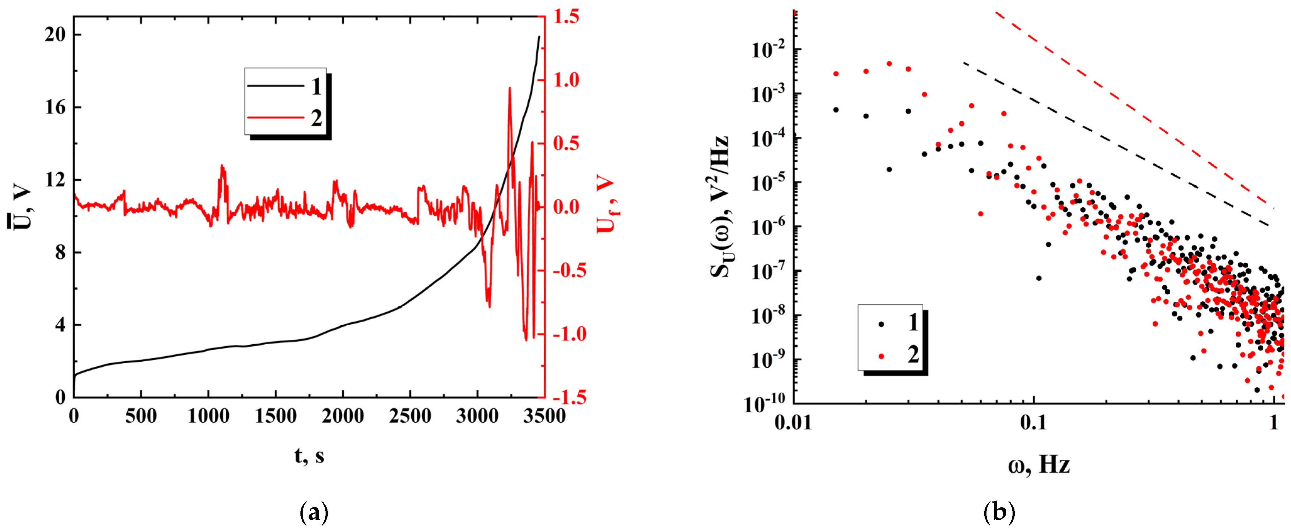
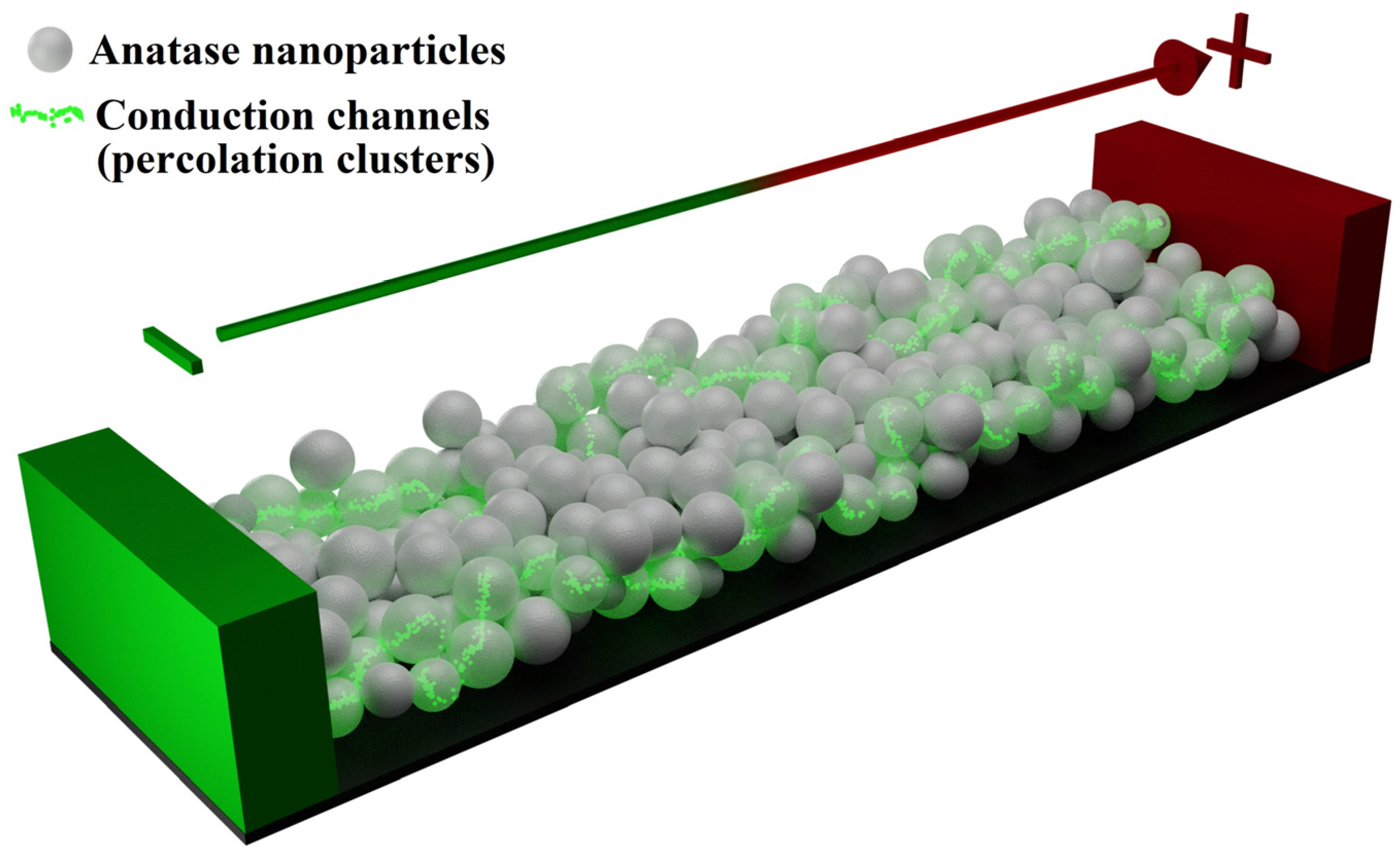
- a long-term quasi-stationary stage II is characterized by a gradual decrease in ohmic conductivity of the bridges (see dataset 1 in Figure 9) due to a decrease in the number of conduction channels previously formed at stage I; this effect can be considered in terms of accumulating decrease in the concentration of electrons due to their capture by deep traps in anatase nanoparticles during electron transport in the bridges;
- (3)
- as the number of conduction channels in the bridges approaches a critical value corresponding to the percolation threshold, a rapid decrease in ohmic conductivity and, accordingly, an abrupt increase in the voltage drops across the studied samples occurs (stage III).
4.4. Spectral Properties of the Noise of Conduction Current
5. Conclusions
Author Contributions
Funding
Data Availability Statement
Acknowledgments
Conflicts of Interest
References
- Witkiewicz, Z.; Jasek, K.; Grabka, M. Semiconductor gas sensors for detecting chemical warfare agents and their simulants. Sensors 2023, 23, 3272. [Google Scholar] [CrossRef] [PubMed]
- Qin, Q.; Olimov, D.; Yin, L. Semiconductor-type gas sensors based on γ-Fe2O3 nanoparticles and its derivatives in conjunction with SnO2 and graphene. Chemosensors 2022, 10, 267. [Google Scholar] [CrossRef]
- Sharma, A.; Ahmed, A.; Singh, A.; Oruganti, S.K.; Khosla, A.; Arya, S. Review—Recent advances in tin oxide nanomaterials as electrochemical/chemiresistive sensors. J. Electrochem. Soc. 2021, 168, 027505. [Google Scholar] [CrossRef]
- Chen, N.; Deng, D.; Li, Y.; Xing, X.; Liu, X.; Xiao, X.; Wang, Y. The xylene sensing performance of WO3 decorated anatase TiO2 nanoparticles as a sensing material for a gas sensor at a low operating temperature. RSC Adv. 2016, 6, 49692–49701. [Google Scholar] [CrossRef]
- Feiyu, D.; Wang, Y. Transition metal oxide nanostructures: Premeditated fabrication and applications in electronic and photonic devices. J. Mater. Sci. 2018, 53, 4334–4359. [Google Scholar]
- Sudarshan, S.; Das, S.; Ray, S.K. Progress in group-IV semiconductor nanowires based photonic devices. Appl. Phys. A 2023, 129, 216. [Google Scholar]
- Baldini, E.; Palmieri, T.; Pomarico, E.; Auböck, G.; Chergui, M. Clocking the ultrafast electron cooling in anatase titanium dioxide nanoparticles. ACS Photonics 2018, 5, 1241–1249. [Google Scholar] [CrossRef]
- Song, Y.; You, K.; Chen, Y.; Zhao, J.; Jiang, X.; Ge, Y.; Wang, Y.; Zheng, J.; Xing, C.; Zhang, H. Lead monoxide: A promising two-dimensional layered material for applications in nonlinear photonics in the infrared band. Nanoscale 2019, 11, 12595. [Google Scholar] [CrossRef]
- Li, J.; Chen, C.; Liu, S.; Lu, J.; Goh, W.P.; Fang, H.; Qiu, Z.; Tian, B.; Chen, Z.; Yao, C.; et al. Ultrafast electrochemical expansion of black phosphorus toward high-yield synthesis of few-layer phosphorene. Chem. Mater. 2018, 30, 2742–2749. [Google Scholar] [CrossRef]
- Terna, A.D.; Elemike, E.E.; Mbonu, J.I.; Osafile, O.E.; Ezeani, R.O. The future of semiconductors nanoparticles: Synthesis, properties and applications. Mater. Sci. Eng. B 2021, 272, 115363. [Google Scholar] [CrossRef]
- Collins, G.; Lonergan, A.; McNulty, D.; Glynn, C.; Buckley, D.; Hu, C.; O’Dwyer, C. Semiconducting metal oxide photonic crystal plasmonic photocatalysts. Adv. Mater. Interfaces 2020, 7, 1901805. [Google Scholar] [CrossRef]
- Xie, X.Q.; Kretschmer, K.; Wang, G.X. Advances in graphene-based semiconductor photo-catalysts for solar energy conversion: Fundamentals and materials engineering. Nanoscale 2015, 7, 13278–13292. [Google Scholar] [CrossRef] [PubMed]
- Yao, S.; Zhang, C.; Xie, F.; Xue, S.; Gao, K.; Guo, R.; Shen, X.; Li, T.; Qin, S. Hybrid membrane with SnS2 nanoplates decorated nitrogen-doped carbon nanofibers as binder-free electrodes with ultrahigh sulfur loading for lithium sulfur batteries. ACS Sustain. Chem. Eng. 2020, 8, 2707–2715. [Google Scholar] [CrossRef]
- Yao, S.; He, Y.; Wang, Y.; Bi, M.; Liang, Y.; Majeed, A.; Yang, Z.; Shen, X. Porous N-doped carbon nanofibers assembled with nickel ferrite nanoparticles as efficient chemical anchors and polysulfide conversion catalyst for lithium-sulfur batteries. J. Colloid Interface Sci. 2021, 601, 209–219. [Google Scholar] [CrossRef]
- Li, J.; Song, P.; Zhao, J.; Vaklinova, K.; Zhao, X.; Li, Z.; Qiu, Z.; Wang, Z.; Lin, L.; Zhao, M.; et al. Printable two-dimensional superconducting monolayers. Nat. Mat. 2021, 20, 181–187. [Google Scholar] [CrossRef] [PubMed]
- Kelly, A.G.; O’Suilleabhain, D.; Gabbett, C.; Coleman, J.N. The electrical conductivity of solution-processed nanosheet networks. Nat. Rev. Mater. 2022, 7, 217–234. [Google Scholar] [CrossRef]
- Scanlon, D.O.; Dunnill, C.W.; Buckeridge, J.; Shevlin, S.A.; Logsdail, A.J.; Woodley, S.M.; Catlow, C.R.A.; Powell, M.J.; Palgrave, R.G.; Parkin, I.P.; et al. Band alignment of rutile and anatase TiO2. Nat. Mater. 2013, 12, 798–801. [Google Scholar] [CrossRef]
- Hanaor, D.A.H.; Sorrell, C.C. Review of the anatase to rutile phase transformation. J. Mater. Sci. 2011, 46, 855–874. [Google Scholar] [CrossRef]
- Tang, H.; Lévy, F.; Berger, H.; Schmid, P.E. Urbach tail of anatase TiO2. Phys. Rev. B 1995, 52, 7771–7774. [Google Scholar] [CrossRef]
- Moser, S.; Fatale, S.; Krüger, P.; Berger, H.; Bugnon, P.; Magrez, A.; Niwa, H.; Miyawaki, J.; Harada, Y.; Grioni, M. Electron-phonon coupling in the bulk of anatase TiO2 measured by resonant inelastic X-ray spectroscopy. Phys. Rev. Lett. 2015, 115, 096404. [Google Scholar] [CrossRef]
- Zimnyakov, D.A.; Yuvchenko, S.A. Effective dielectric function of TiO2 nanoparticles under laser pumping in the fundamental absorption band. Quantum Electr. 2017, 47, 547–552. [Google Scholar] [CrossRef]
- Zimnyakov, D.A.; Yuvchenko, S.A.; Volchkov, S.S. Effective dielectric function of laser-pumped anatase nanoparticles: Influence of free carriers trapping and depletion of valence band. Opt. Exp. 2018, 26, 32941–32957. [Google Scholar] [CrossRef] [PubMed]
- Merck. Available online: https://www.sigmaaldrich.com/RU/en/product/aldrich/637254 (accessed on 15 October 2022).
- Williamson, G.K.; Hall, W.H. X-ray line broadening from filed aluminium and wolfram. Acta Metall. 1953, 1, 22–31. [Google Scholar] [CrossRef]
- Rabiei, M.; Palevicius, A.; Monshi, A.; Nasiri, S.; Vilkauskas, A.; Janusas, G. Comparing methods for calculating nano crystal size of natural hydroxyapatite using X-ray diffraction. Nanomaterials 2020, 10, 1627. [Google Scholar] [CrossRef] [PubMed]
- Gingold, D.B.; Lobb, C.J. Percolative conduction in three dimensions. Phys. Rev. B 1990, 42, 8220–8224. [Google Scholar] [CrossRef] [PubMed]
- Clerc, J.-M.; Podolskiy, V.A.; Sarychev, A.K. Precise determination of the conductivity exponent of 3D percolation using exact numerical renormalization. Eur. Phys. J. B 2000, 15, 507–516. [Google Scholar] [CrossRef]
- Kozlov, B.; Laguës, M. Universality of 3D percolation exponents and first-order corrections to scaling for conductivity exponents. Phys. Stat. Mech. Its Appl. 2000, 389, 5339–5346. [Google Scholar] [CrossRef]
- Grassberger, P. Conductivity exponent and backbone dimension in 2-d percolation. Phys. Stat. Mech. Its Appl. 1999, 262, 251–263. [Google Scholar] [CrossRef]
- Cen, W.; Liu, D.; Mao, B. Molecular trajectory algorithm for random walks on percolation systems at criticality in two and three dimensions. Phys. Stat. Mech. Its Appl. 2012, 391, 925–929. [Google Scholar] [CrossRef]
- MacKinnon, A. Critical exponents for the metal-insulator transition. J. Phys. Condens. Matter 1994, 6, 2511–2518. [Google Scholar] [CrossRef]
- Lebedev, E.A.; Dittrich, T. Space charge limited current in porous silicon and anatase (TiO2). Semiconductors 2002, 36, 1268–1271. [Google Scholar] [CrossRef]
- Sellers, M.C.K.; Seebauer, E.G. Measurement method for carrier concentration in TiO2 via the Mott–Schottky approach. Thin Solid Film. 2011, 519, 2103–2110. [Google Scholar] [CrossRef]
- Kytin, V.; Dittrich, T.; Koch, F.; Lebedev, E. Injection currents and effect of negative capacitance in porous TiO2. Appl. Phys. Lett. 2001, 79, 108–110. [Google Scholar] [CrossRef]
- Maxwell Garnet, J.C. Colours in metal glasses and in metallic films. Philos. Trans. R. Soc. 1904, A203, 385–420. [Google Scholar]
- Dubrov, V.E.; Levinshtein, M.E.; Shur, M.S. Permittivity anomaly in metal-dielectric transitions. Theory and simulation. Zh. Exp. Teor. Fiz. 1976, 70, 2014–2024. [Google Scholar]
- Castner, T.G.; Lee, N.K. Dielectric anomaly and the metal-insulator transition in n-type silicon. Phys. Rev. Lett. 1975, 34, 1627–1630. [Google Scholar] [CrossRef]
- Efros, A.L.; Shklovskii, B.I. Critical behaviour of conductivity and dielectric constant near the metal-non-metal transition threshold. Phys. Stat. Sol. B 1976, 76, 475–485. [Google Scholar] [CrossRef]


Disclaimer/Publisher’s Note: The statements, opinions and data contained in all publications are solely those of the individual author(s) and contributor(s) and not of MDPI and/or the editor(s). MDPI and/or the editor(s) disclaim responsibility for any injury to people or property resulting from any ideas, methods, instructions or products referred to in the content. |
© 2023 by the authors. Licensee MDPI, Basel, Switzerland. This article is an open access article distributed under the terms and conditions of the Creative Commons Attribution (CC BY) license (https://creativecommons.org/licenses/by/4.0/).
Share and Cite
Zimnyakov, D.A.; Volchkov, S.S.; Vasilkov, M.Y.; Plugin, I.A.; Varezhnikov, A.S.; Gorshkov, N.V.; Ushakov, A.V.; Tokarev, A.S.; Tsypin, D.V.; Vereshagin, D.A. Semiconductor-to-Insulator Transition in Inter-Electrode Bridge-like Ensembles of Anatase Nanoparticles under a Long-Term Action of the Direct Current. Nanomaterials 2023, 13, 1490. https://doi.org/10.3390/nano13091490
Zimnyakov DA, Volchkov SS, Vasilkov MY, Plugin IA, Varezhnikov AS, Gorshkov NV, Ushakov AV, Tokarev AS, Tsypin DV, Vereshagin DA. Semiconductor-to-Insulator Transition in Inter-Electrode Bridge-like Ensembles of Anatase Nanoparticles under a Long-Term Action of the Direct Current. Nanomaterials. 2023; 13(9):1490. https://doi.org/10.3390/nano13091490
Chicago/Turabian StyleZimnyakov, Dmitry A., Sergey S. Volchkov, Mikhail Yu. Vasilkov, Ilya A. Plugin, Alexey S. Varezhnikov, Nikolay V. Gorshkov, Arseni V. Ushakov, Alexey S. Tokarev, Dmitry V. Tsypin, and Dmitry A. Vereshagin. 2023. "Semiconductor-to-Insulator Transition in Inter-Electrode Bridge-like Ensembles of Anatase Nanoparticles under a Long-Term Action of the Direct Current" Nanomaterials 13, no. 9: 1490. https://doi.org/10.3390/nano13091490