Article

Investigation of TiO2 Deposit on SiO2 Films: Synthesis, Characterization, and Efficiency for the Photocatalytic Discoloration of Methylene Blue in Aqueous Solution

by
Yuliana de Jesús Acosta-Silva
1,*,
Manuel Toledano-Ayala
1,
Salvador Gallardo-Hernández
2,
Luis A. Godínez
3 and
Arturo Méndez-López
1,*
1
Research and Postgraduate Division, Faculty of Engineering, Autonomous University of Queretaro (UAQ), University Center, Querétaro 76010, Mexico
2
Department of Physics, Center for Research and Advanced Studies of the National Polytechnic Institute, México City 07360, Mexico
3
Centro de Investigación en Química para la Economía Circular, CIQEC, Faculty of Chemistry, Autonomous University of Queretaro, University Center, Querétaro 76010, Mexico
*
Authors to whom correspondence should be addressed.
Nanomaterials 2023, 13(8), 1403; https://doi.org/10.3390/nano13081403
Submission received: 13 March 2023 / Revised: 5 April 2023 / Accepted: 11 April 2023 / Published: 19 April 2023
(This article belongs to the Topic Advances in Functional Thin Films)

Abstract

:
TiO2-SiO2 thin films were created on Corning glass substrates using a simple method. Nine layers of SiO2 were deposited; later, several layers of TiO2 were deposited, and their influence was studied. Raman spectroscopy, high resolution transmission electron spectroscopy (HRTEM), an X-ray diffractometer (XRD), ultraviolet-visible spectroscopy (UV-Vis), a scanning electron microscope (SEM), and atomic force microscopy (AFM) were used to describe the sample’s shape, size, composition, and optical characteristics. Photocatalysis was realized through an experiment involving the deterioration of methylene blue (MB) solution exposed to UV-Vis radiation. With the increase of TiO2 layers, the photocatalytic activity (PA) of the thin films showed an increasing trend, and the maximum degradation efficiency of MB by TiO2-SiO2 was 98%, which was significantly higher than that obtained by SiO2 thin films. It was found that an anatase structure was formed at a calcination temperature of 550 °C; phases of brookite or rutile were not observed. Each nanoparticle’s size was 13–18 nm. Due to photo-excitation occurring in both the SiO2 and the TiO2, deep UV light (λ = 232 nm) had to be used as a light source to increase photocatalytic activity.

1. Introduction

Diverse colors and other organic and inorganic contaminants are found in textile industry wastewater. Twelve percent of synthetic textile dyes, including eriochorome black-T (EBT), methyl orange (MO), rhodamine B, and methylene blue (MB), are thought to be lost during the dyeing process, and approximately 20% of these dyes are carried as waste to industrial wastewater treatment facilities [1]. Among these chemicals, MB is one of the most popular, as it is used not only as a dye for wool, hair coloring compounds, paper prints, and cotton, but also as an antiseptic, among other health-related purposes [2]. MB, on the other hand, is regarded as biologically dangerous, because it is a powerful carcinogen for marine animals, and in humans severely irritates the eyes, causes convulsions, irritates sensitive skin, and induces tachycardia [3]. MB also reacts with various substances, which makes the treatment of aqueous effluents containing MB a difficult task [4]. On the other hand, advanced oxidation processes (AOPs) are regarded as efficient approaches for the elimination of organic contaminants from aqueous solutions, such as MB. These procedures are based on the fact that hydroxyl radicals (HO), which have a particularly high oxidation potential, rapidly oxidize the majority of organic contaminants with great efficiency (generally in the range 108–1011 M−1 s−1) [5,6,7]. One way to produce OH radicals is by the oxidation of surface adsorbed H2O molecules, using photo-excited semiconductor materials [8]. Titanium dioxide (TiO2) is an excellent photocatalyst, due to its low cost, nontoxicity, and good chemical and mechanical stability [9,10]. Therefore, TiO2 is used in solar cells [11], self-cleaning glasses [12], antifogging windows [13], and as a photocatalytic material for the degradation of contaminants in wastewater [14]. The ability of illuminated TiO2 to produce OH radicals depends on specific features of TiO2, such as the size of the semiconductor crystallites and their surface area [15]. The photo-physical and chemical properties of the TiO2 material allows for coupling to other semiconductors; in this regard, SiO2 is a practical option because of its great mechanical strength and good thermal stability [16]. Amorphous SiO2 has also been demonstrated to have a high surface area and outstanding adsorption capacity, making it an effective substrate for semiconductor films [17]. Zhou et al., for example, demonstrated that mixed metal oxides (TiO2-SiO2) improve the photocatalytic efficiency of the individual materials, because it enhances the materials’ adsorption properties and increases their concentration of surface hydroxyl groups in the thin film. In addition, SiO2 was shown to promote a large surface area and an appropriately porous structure [15]. There are abundant reports in the literature focusing on the synthesis and characterization of TiO2-based photocatalysts; in this context, we believe that in addition to phase structure, doping, and composite design and synthesis, the study of TiO2 layers grown by the sol–gel dip-coating method on top of the SiO2 semiconductor material films could be useful for the development of novel and efficient photocatalytic surfaces. This communication, therefore, presents the structural, morphological, and optical properties of the SiO2/TiO2 composite films proposed, as well as an exploration of their photocatalytic performance.

2. Experimental Details

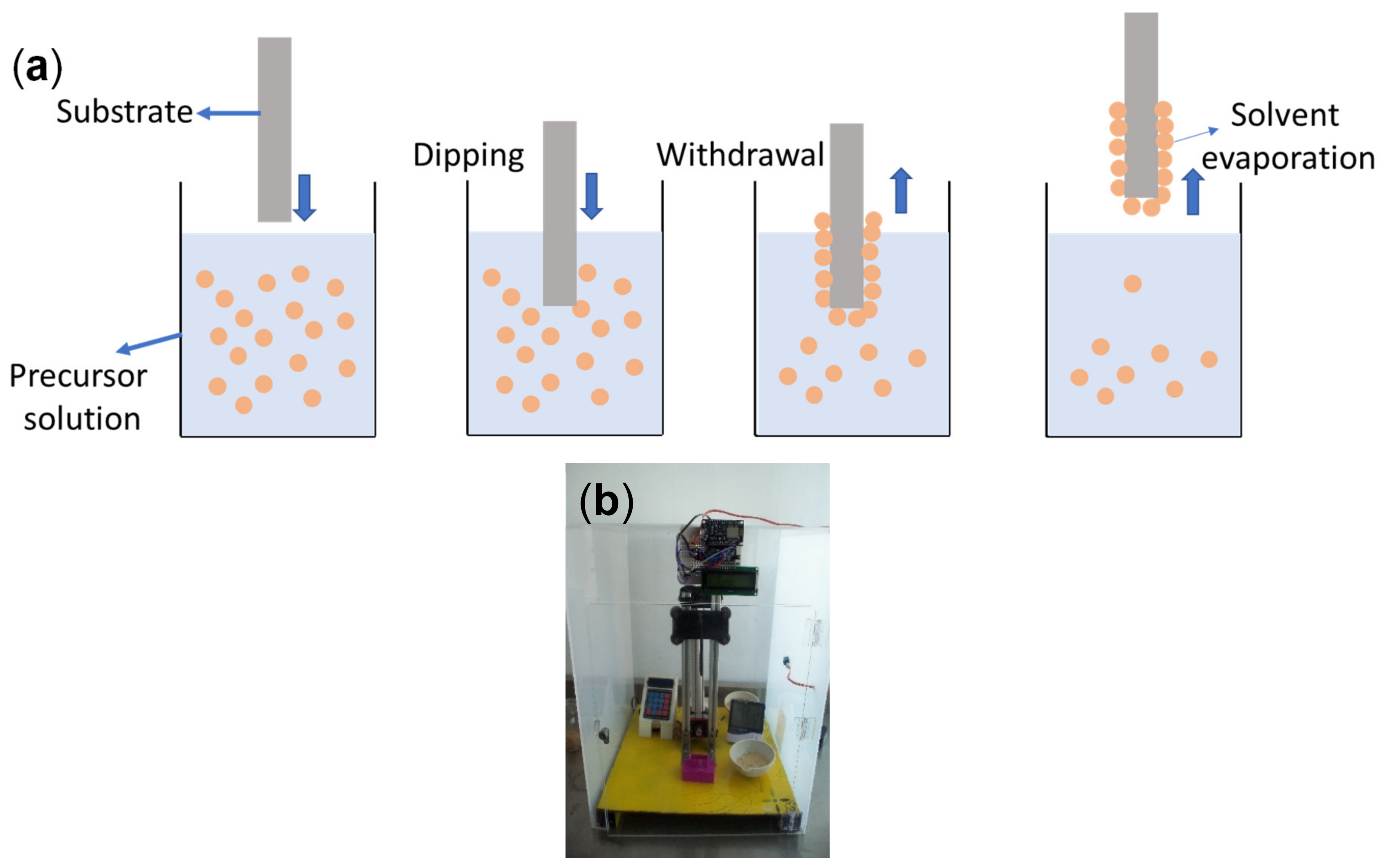
2.1. SiO2 Thin Films

SiO2 solutions were prepared by dissolving a certain amount of triblock copolymer (BASF, EO106-PO70-EO106, F127) in ethanol (J.T. Baker, Querétaro, Mexico), with constant stirring for 1 h at 37 °C. Then, 0.7 mL of HCl (J.T. Baker) were added by drops, and the solution was continuously stirred for 30 min. After adding 5.5 mL of TEOS to the mixture, it was agitated for 24 h at 36 °C. The resulting transparent and homogeneous phase was then employed to prepare thin films on glass substrates (Corning 2947, area 2.5 × 7.5 cm2) using the dip-coating technique. Figure 1a shows a scheme describing the dip-coating process employed in this work. The previously cleaned substrate is dipped into a solution of the precursors (the material to be deposited) and then withdrawn vertically at a controlled speed. For this purpose, the homemade system shown in Figure 1b (operating at a withdrawal rate of 8 cm/min) was utilized to obtain SiO2 thin films containing nine sequential coatings; each layer was prepared by drying the coating at 250 °C for 2 h in an open atmosphere. Subsequently, the temperature was increased to 550 °C (calcination temperature) over two hours at a rate of 2 °C/min ramp.

2.2. TiO2-SiO2 Thin Films

Thin films were prepared by immersion as reported in a previous section, in a solution containing titanium (IV) isopropoxide (Sigma-Aldrich Co., Querétaro, Mexico), 2-propanol (J.T. Baker), and hydrochloric acid (37% HCl). The TiO2 thin films were deposited using the 2 cm/min removal rate for the dip coating process, and in this case, the films surveyed consisted of coatings of 5, 7, and 9 layers. As was indicated for the SiO2 films, each layer was dried at 250 °C for 3 min, and once each film was completed with the corresponding number of layers, the surface modified material was calcined at 550 °C for 1 h. In terms of the cross-sectional characterization of the composite films under study, we carried out thickness measurements using a KLA TENCO P-15 profilometer as described in the experimental section. In this way, while the thickness of the SiO2 films under study corresponded to ~250 nm, the thicknesses of the TiO2 material films consisted of ~171, 219, and 262 nm, depending on the number of deposited TiO2 layers (5, 7 and 9, respectively).

2.3. Structural, Optical, and Morphological Characterization of the Films

UV-Vis measurements were carried out using an Evolution 220 UV-Vis Spectrophotometer. X-ray diffraction experiments were carried out using a Philips X-ray diffractometer (PANalytical’s X’pert PRO X-ray diffractometer, Malvern, UK) that employs a Cu-Kα radiation with a wavelength of 0.15405 nm in the 20 ≤ 2θ ≤ 80° range. The voltage and current settings were 30 kV and 40 mA, respectively. The samples were continuously scanned with a step size of 0.02° (2θ) and a count time of 1 s per step. Structural properties were also studied using Raman spectroscopy that collected data using a Labram-Dilor Raman spectrometer equipped with a He-Ne laser exciting source, operating between the wavelengths of 200 and 800 nm at ambient temperature (AT). The roughness and surface topography were examined by AFM (Park Scientific Inst. System, Suwon, South Korea). Using a scanning electron microscope (SEM, JEOL JSM-6300, Tokyo, Japan), surface pictures were acquired. Prior to the acquisition of images by high-resolution transmission electron microscopy, tiny bits of films were scraped. JEOL JEM 2010 microscope with an acceleration voltage of 200 kV was used for this objective. Typically, the magnification ranged from ×400,000 to ×500,000. At the camera length L = 20 cm, selected area electron diffraction (SAED) was carried out. Thickness measurements were made using a KLA TENCOR P-15 profilometer (Milpitas, CA, USA).

2.4. Photocatalytic Activity Evaluation

The PA of films was determined at AT by assessing the MB discoloration kinetics of aqueous solutions of 5.4 mg/L (1.88 × 10⁻⁵ mol/L) under UV radiation. In this way, 3 mL of the aqueous MB solution were poured into a standard quartz cell, and later, a TiO2-SiO2 coated substrate was placed vertically inside the cell (with a 2 cm2 exposed area). Five quartz cells prepared in this way were used for each thin film under study. The 15 W lamp used to produce the irradiation light had a 254 nm wavelength (G15T8 germicidal lamp as the exciting source). Five centimeters separated the quartz cells from the lamp. A Thermo ScientificTM Evolution 220 Spectrophotometer was used to measure the optical absorbance of the test solution every 60 min for the course of the 5 h of total irradiation. The absorbance peak reduction for MB was examined in the range of 400 to 800 nm. The residual methylene blue concentration was calculated using the absorbance data at 664 nm employing the Beer-Lambert’s law.

3. Results and Discussion

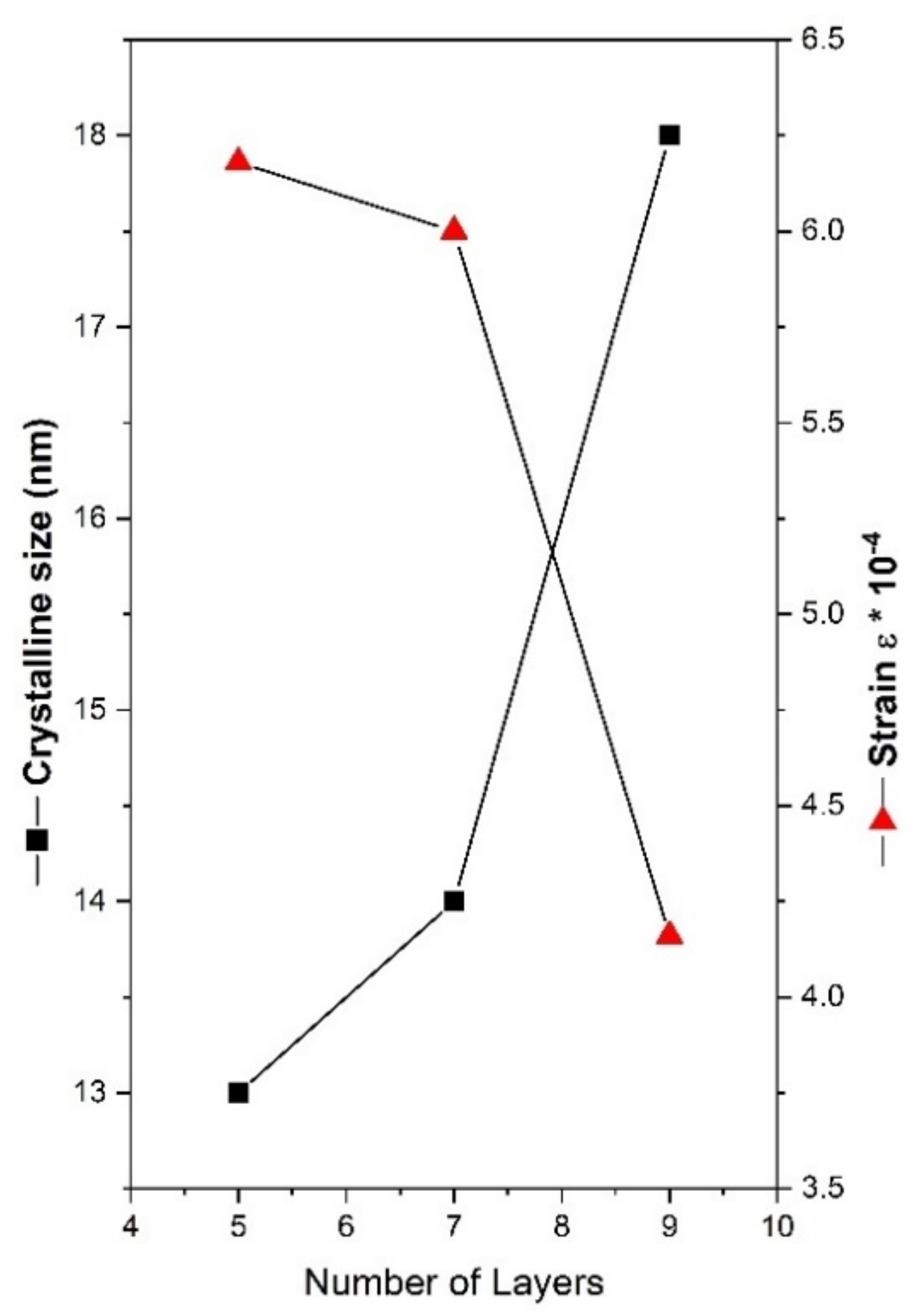
3.1. X-ray Diffraction
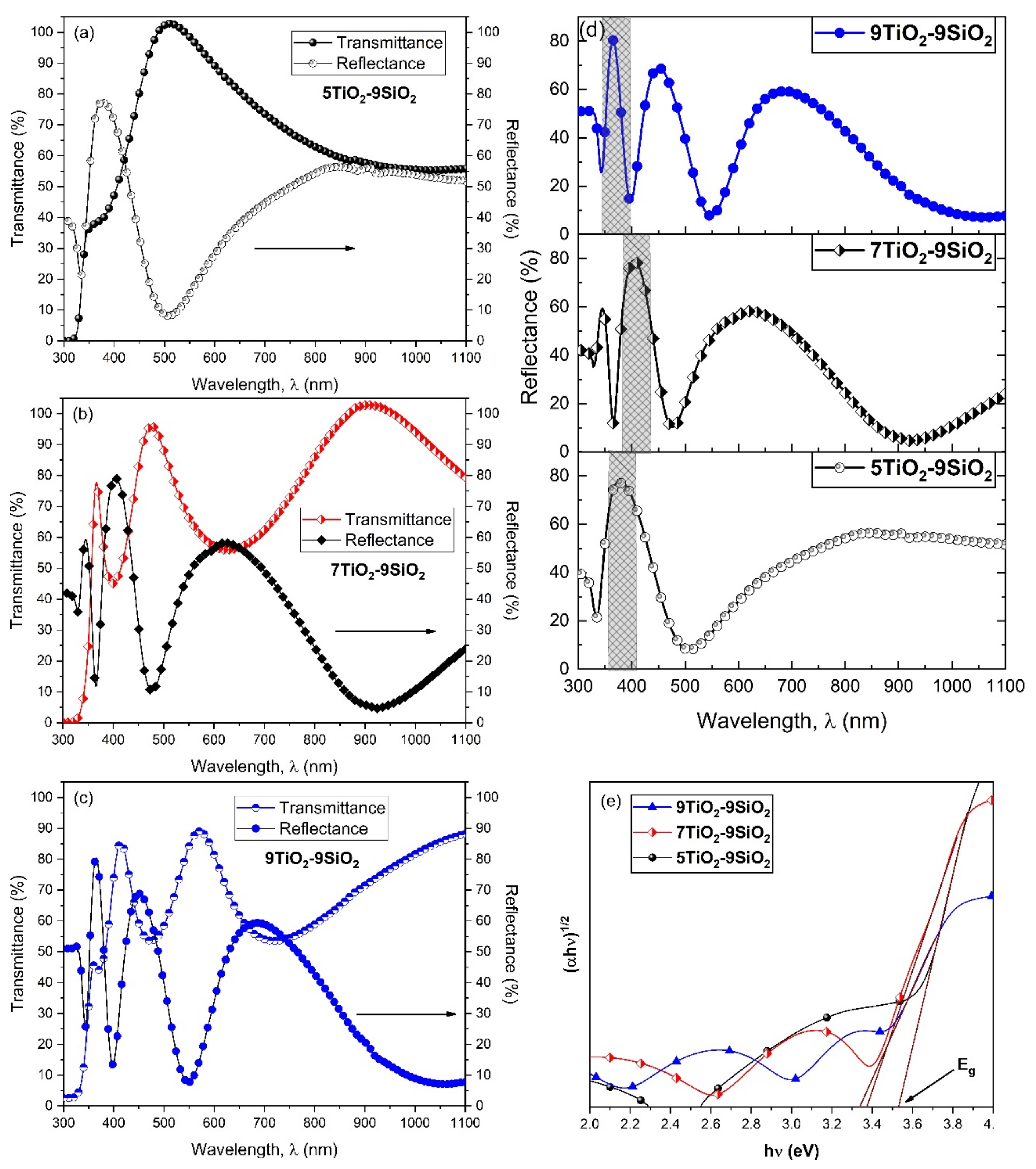
The XRD patterns of the thin films of TiO2 deposited on mesoporous SiO2 thin films are shown in Figure 2. The JCPDS-ICDD powder diffraction database was used to identify the crystal phases and matching miller indices. The JCPDF number for TiO2 is 00-21-1272. The anatase phase of TiO2 predominated in all the samples’ patterns; no other phase was present. The samples diffraction peaks were seen at 2θ values of 25.3°, 37.8°, 38.6°, 48.1°, 53.9°, 55.1°, 62.7°, 68.9°, 70.4°, and 75.1° and could be perfectly correlated with the (101), (004), (112), (200), (105), (211), (204), (116), (220), and (215) crystal planes of anatase TiO2. All peaks were well indexed according to the standard patterns. The increase in the number of TiO2 coatings resulted in thin films that exhibited higher intensities, indicating an increase in crystallinity owing to the higher presence of TiO2 layers on top of SiO2. No phase transformation occurred for any of the samples. Moreover, all samples displayed a preferential orientation growth at (101) the plane (see Figure 2), which can be attributed to the plane’s low surface energy value [18]. According to Zhang et al. [19], the phase transformation of TiO2 only takes place at temperatures above 900 °C. An estimation of average crystallite size was calculated using the Scherrer equation; 5TiO2-9SiO2, 7TiO2-9SiO2, and 9TiO2-9SiO2 samples correspond to 13, 14, and 18 nm, respectively. For these calculations, Equation (1) was used as follows [20]:
d = K λ β cos θ  
λ the wavelength of the radiation (1.54056 for CuK radiation), θ is Bragg’s angle, β the full width at half maximum (FWHM) intensity in radians, d the average thickness of the crystal in a direction normal to the diffracting plane (hkl), and K is Scherrer constant. Equations (2) and (3), respectively, express two additional structural parameters known as the dislocation density (δ) and the microstrain (ε) [21]:
δ = 1 d 2  
ε = β 4 tan θ  
Figure 3 illustrates how the number of layers of TiO2 affected the variance in dislocation density, crystallite size, and strain in the thin films studied. The following values demonstrate that the strain decreases as the number of layers are enhanced and the crystallite size increases. The same trend of the crystallite size was also reported by Lin et al. [22] for ZnO films made with various thicknesses. The relationship between the two variables can be explained by the collective fusing of small crystallite particles into larger ones, which leads to decreased densities of nucleation centers and, in turn, internal strain [23,24].

3.2. UV-Vis

Based on the UV-vis characterization experiments, transmittance (T), and reflectance (R) data on the TiO2-SiO2 thin films were obtained in the 300–1100 nm wavelength window. Figure 4a–c shows that transmittance spectra are characterized by maxima and minima values of different orders. As the film thickness increases (to 5, 7, and 9 layers), the location of a particular transmittance extrema (maxima) shifts towards longer wavelengths. Similar results have been reported for five TiO2 layers on SiO2 [25]. Also, the thin films under investigation displayed a dramatic decline in transmittance in the ultraviolet spectrum. It was found that the absorption edge of the transmittance moves towards red in the ultraviolet region as the film thickness grows for TiO2 thin films produced with the same withdrawal speed. Figure 4d shows the optical reflectance as a function of wavelength (λ). When there is an increase in the number of layers, the reflectance rises, which is more significant within the visible region. The band gap between conduction (CB) and valence bands (VB), a crucial optical characteristic of thin films, is calculated using the well-known Tauc equation, as given in Equation (4) [26]:
α h ν = A h ν E g n
Here, the constant A is related to the effective masses (electrons and holes), the input photon energy is represented by hν, the optical bandgap is represented by E g , and the exponent n is dependent on the kind of traνnsition. When n = 2 denotes permitted indirect transitions, 3 denotes forbidden indirect transitions, 1/2 denotes permissible direct transitions and 3/2 for forbidden direct transitions. When the line is intercepted at the energy axis (α = 0) yields the band gap (Figure 4e). Here, it can be shown that the E g values decrease as the number of TiO2 layers increases. The E g value for 9TiO2-9SiO2 was found to be 3.34 eV, as shown in Figure 4e, which is comparable to observations reported by other groups [27,28,29]. The bandgap energy in Figure 4e for 5TiO2 is 3.53 eV, and in this regard, it has been reported that for powders light absorption (as well as the bandgap of TiO2), does not change when several layers of TiO2 are present. For interacting semiconductor layers, however, it is common to observe a decrease in the band gap due to an increase in the grain size of TiO2 layers [30]. Also, some sub-bands form due to defect levels in the forbidden band of TiO2, thereby reducing the “band-gap energy” [31].

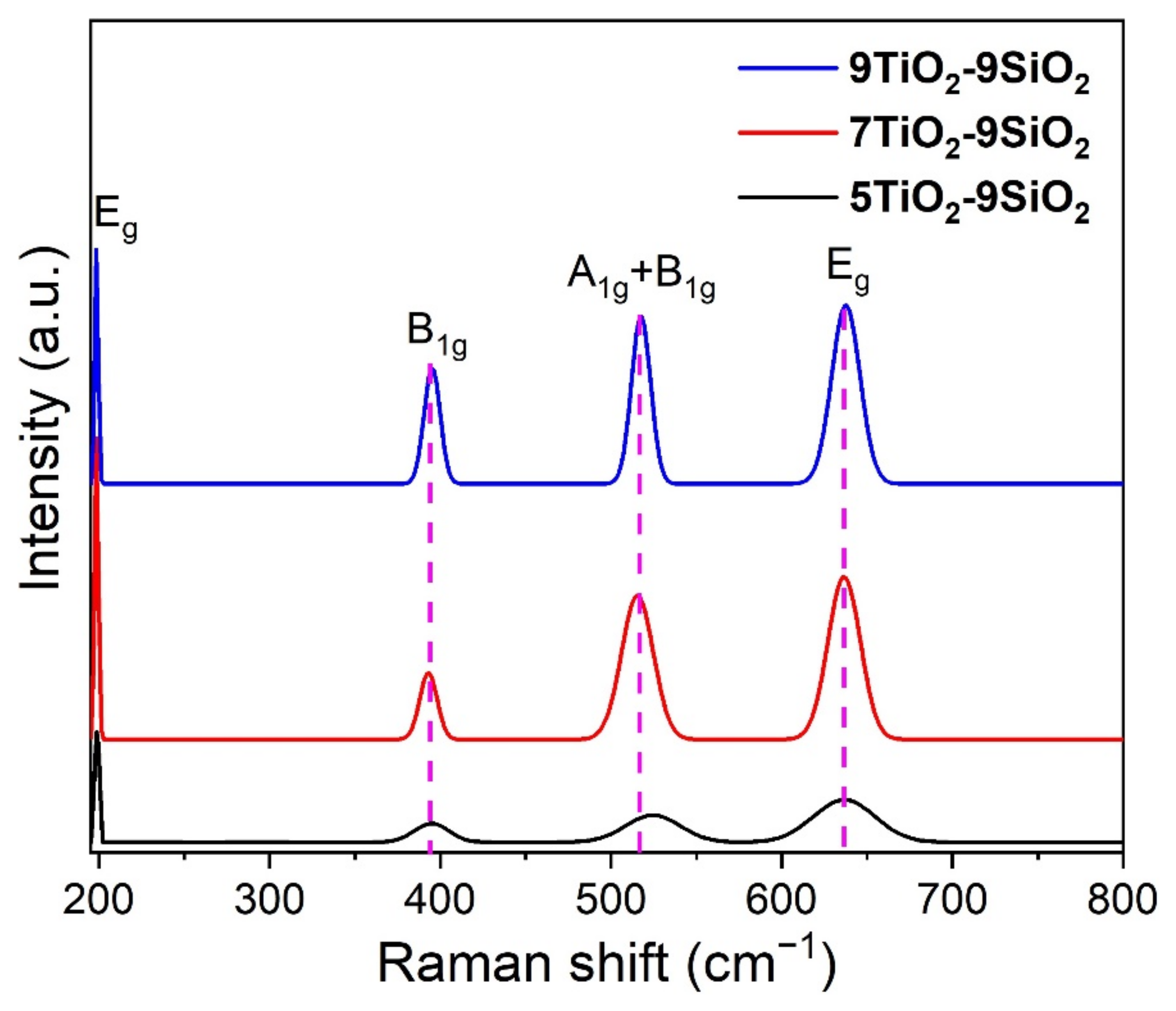
3.3. Raman Spectroscopy

Raman measurements of the layers of TiO2 deposited on mesoporous SiO2 were investigated as described in the experimental section. The resulting Raman data in the 190–800 cm−1 range (Figure 5) show that the anatase titania vibrational modes E g , B1g, A1g+B1g, and E g have been assigned to peaks at 197, 394, 516, and 637 cm−1 in all samples, respectively [32,33]. While the peaks located at 197 and 637 cm−1 agree with the E g mode (attributed to the symmetric stretching vibration of O-Ti-O) and a B1g mode corresponds to the peak at 394 cm−1 (which is due to the symmetric bending vibration of O-Ti-O), the A1g mode arises from the asymmetric bending vibration of this same bond. The latter mode also overlaps with the remaining B1g mode, producing the emission of a signal with a peak at 516 cm−1. This mode was extensively investigated by Otakar et al. [33]. The intensity of the peaks is normally affected by the number of layers [34]. The Raman spectra obtained indicate that the surface of the TiO2 thin films is characterized by a pure anatase phase without the production of impurity phases, because there are no rutile (447 and 612 cm−1) [35] or brookite (246 and 449 cm−1) [36] phase peaks present. As was previously discussed, these results are consistent with XRD data.

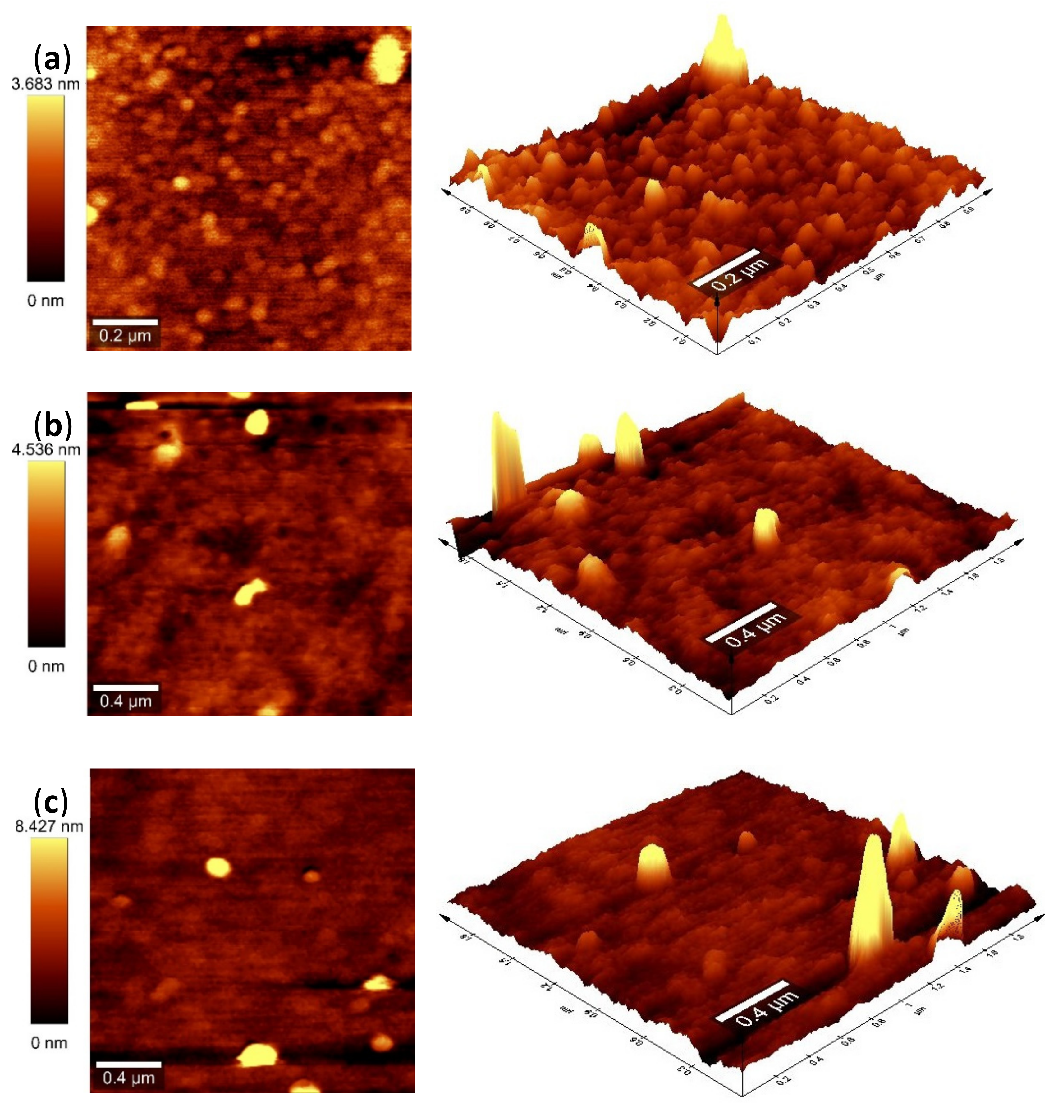
3.4. Atomic Force Microscopy (AFM)

The TiO2-SiO2 thin films that were deposited on Corning glass are depicted in Figure 6 in both two- and three-dimensional AFM pictures. The surface morphologies of the films under study reveals porous structures that, interestingly, are characterized by different roughness. Figure 6a shows that 5TiO2-9SiO2 films are composed by monodisperse spherical particles of a diameter 3.683 nm with a mesoporous structure [37,38]. The main benefit of the reverse micellar route by hydrolysis of titanium isopropoxide to produce TiO2 nanoparticles is monodispersity [39]. In this way, the hydration of surfactant polar heads by water molecules is in competition with the hydrolysis process. Growth restrictions and homogeneous particle sizes are caused by the surfactant molecule restructuring that surround the polar species produced during hydrolysis [37]. It is also observed from Figure 6b,c that the 7TiO2-9SiO2 and 9TiO2-9SiO2 thin films also have granular microstructures which are composed of ~4.53 nm and ~8.43 nm spheric crystals, respectively. AFM image analysis showed the values of surface roughness in addition to crystal diameter. The root mean square roughness values (Rrms) of 5TiO2-9SiO2, 7TiO2-9SiO2 and 9TiO2-9SiO2 correspond to 0.508, 0.177 and 0.076 nm, respectively.

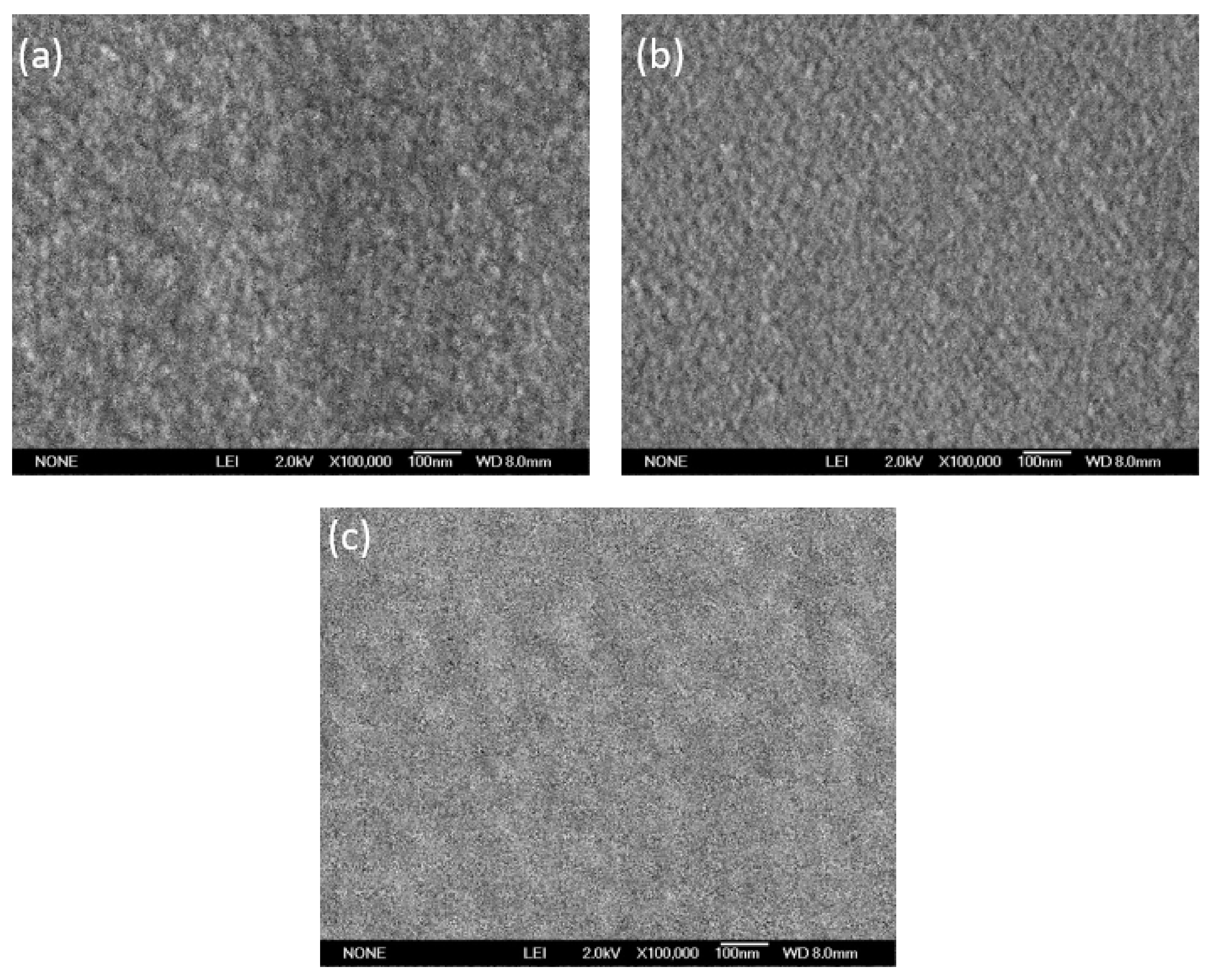
3.5. Scanning Electron Microscope (SEM)

Figure 7 shows the micrographs of thin films. The films under study were annealed at 550 °C; it was observed that the shapes of the formed grains appear to vary according to the number of layers. The most significant differences between the three samples were observed for five layers of TiO2 (Figure 7a), seven layers (Figure 7b), and nine layers (Figure 7c). We observed that by increasing the thickness of the TiO2 films, crack formation did not take place, suggesting not only a relatively strong structure, but also that an increase in the film thickness did not lead to detachment of the deposited layers. For the 5TiO2-9SiO2 thin film (Figure 7a), less closely packed TiO2 particles were dispersed, and a sizable particle increase was observed. As the deposition of the layers in the 7TiO2-9SiO2 sample (Figure 7b) increased, densely packed and uniform nanoscale particles were observed; similar results have been reported in previous studies of TiO2/SiO2 films [40]. The image of the 9TiO2-9SiO2 thin film (Figure 7c) shows an extremely smooth surface involving tiny and dense grains positioned on the surface of the film. These results are comparable to those mentioned by Binyu Yu et al. [41].

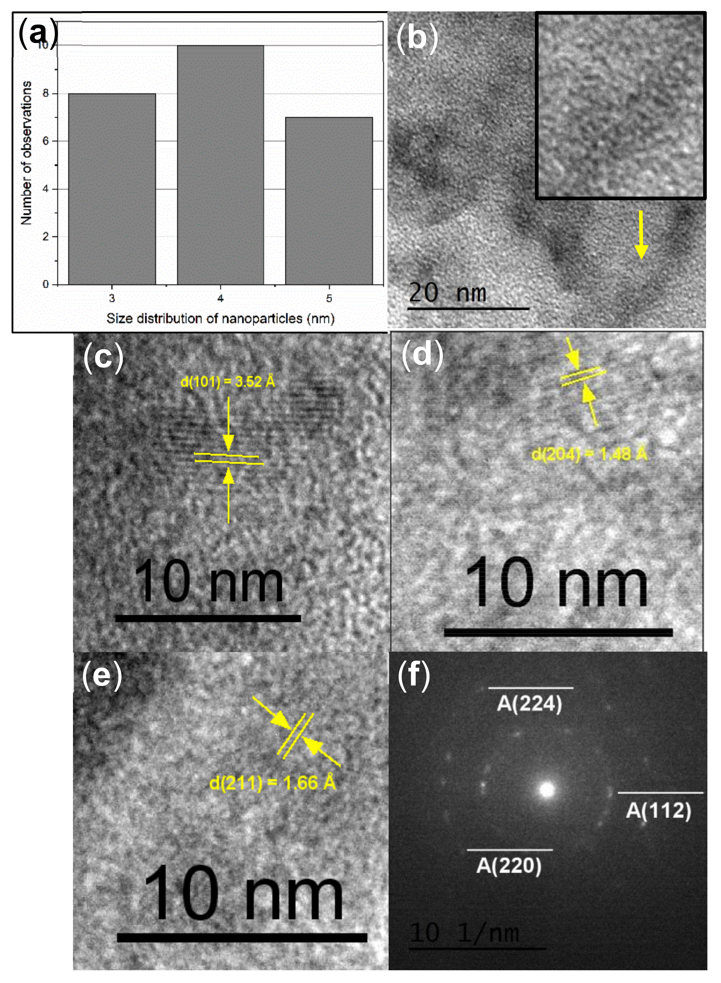
3.6. High Resolution Transmission Electron Spectroscopy (HRTEM)

7TiO2-9SiO2 thin films were examined using High-resolution TEM (HRTEM) to evaluate their crystalline or amorphous. Size distribution analysis shown in Figure 8a reveals that the average diameter and standard deviation of 7TiO2-9SiO2 nanoparticles on the surface of the film are about 3–5 nm—a value range that is not consistent with that calculated from XRD experiments. The Scherrer equation, however, is well known to produce a good approximation, and in this regard, the disordered wormhole-like pore structure of the dip-coating prepared sample was confirmed by TEM (see Figure 8b). This material is a good illustration of the type of molecular sieve in which the atomic organization is disordered similarly to amorphous or mesoporous silica, and the channel structure displays a disordered pattern of micropores with a high specific surface area. High-resolution TEM (HRTEM) images of 7TiO2-9SiO2 in Figure 8c–e revealed the crystalline nature of the nanostructures under study with lattice fringe spacing of 3.52 Å, 1.48 Å, and 1.66 Å, respectively. These can be indexed to (101), (204), and (211) planes of anatase TiO2. Figure 8f, on the other hand, shows the transmission electron diffraction pattern of a 7TiO2-9SiO2 sample. From electron diffraction measurements, the interplanar distances (d) of 7TiO2-9SiO2 samples were determined to be 2.33 Å, 1.33 Å and 1.16 Å. This result corresponds to anatase phase of TiO2. The interplanar distance and the diffraction planes were identified using the powder diffraction files (PDF) #00-021-1272.

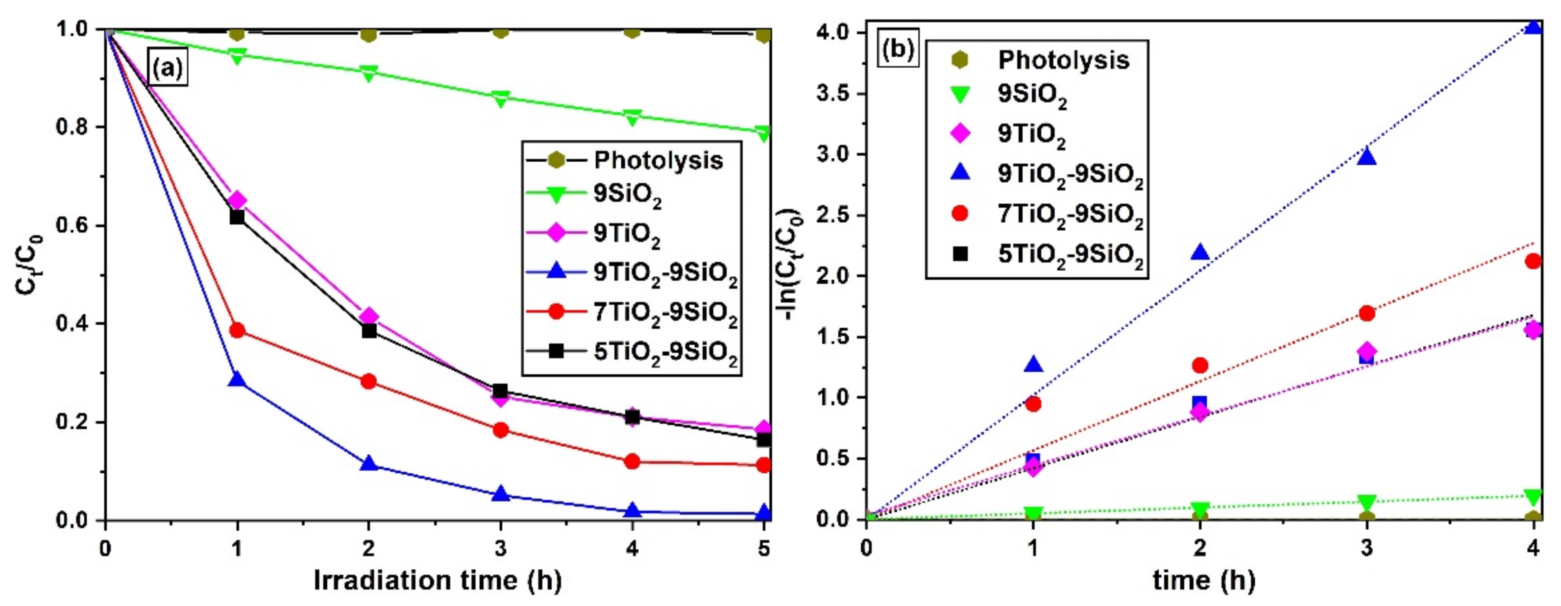
3.7. Degradation of MB with SiO2-TiO2 Photocatalyst under UV Irradiation

The main by-products and most worrying pollutants in the textile industry are organic dyes, which are known to degrade when exposed to high levels of photocatalytic activity (PA) in mesoporous TiO2. It is particularly important to consider a good excitation during photocatalysis, as the energy of the E g must be exceeded. The TiO2 anatase phase has an E g of 3.2 eV, and the corresponding wavelength value of 387 nm showed that light with shorter wavelengths is needed for this project; a wavelength value of 254 nm was selected. TiO2 is excited by UV radiation, resulting in valence band holes that oxidize OH- ions or H2O to produce the hydroxyl radical (·OH) species. The compound is an extremely potent oxidant that easily oxidizes most organic molecules, converting them to CO2, water, and salts [42]. Nevertheless, to improve the absorption efficiency of the TiO2, it must be hydrated with some additive, such as P2O5, carbon, or SiO2 [43]. In this work we have deposited SiO2 thin films on Corning glass substrates, subsequently, various layers of TiO2 were deposited. The opportunity for the hydroxyl radical (·OH) and dye molecules to react during the PA can be enhanced if the thin films absorb more color molecules. The decision was made to utilize the photodegradation of MB to assess the PA of TiO2-SiO2 thin films for dye discoloration applications. UV/Vis spectroscopy was used to determine the solution’s time-dependent MB concentration. Figure 9a plots the normalized MB concentration under UV radiation as a function of time in the absence of any photocatalyst, in the presence of SiO2, and utilizing various concentrations of thin films. The ratio of Ct/C0 at time t = 0 is calculated as 1, using C0 as the initial MB concentration, and Ct corresponds to the concentration of unreacted dye at various times. Figure 9a clearly shows that while photolysis does not result in noticeable dye discoloration, MB concentration decreases roughly 20% after 5h for SiO2 films, reaching substantially more extensive and faster discoloration performances when using TiO2-SiO2 films. Since 5TiO2-9SiO2 materials showed similar activity to that observed for 9TiO2 thin films (in which SiO2 is not present) and since the photocatalytic activity of TiO2-SiO2 increases as the number TiO2 layers on SiO2 is larger, it is possible to suggest that SiO2 acts not only as TiO2 support in these PA films but as a functional semiconductor layer in the hetero-semiconducting film. As observed from the data in Figure 9a, increasing the number of TiO2 layers results in faster discoloration kinetic curves [44,45]. A detailed investigation of the function that particle size plays in pure TiO2 photocatalysts under UV light (wavelength 310–330 nm) was made by Zhang et al. They discovered that the kinetics of the electron/hole recombination process depended critically on particle size [44]. According to Afshar et al., the challenges brought on by the drawbacks of pure titanium powder require the manufacture of modified titania. They found that an increased surface area and interaction regions between the SiO2 and the titanium nanoparticles could result in a combined impact that can be the primary cause of the high activity of TiO2-SiO2 [45].
In gas-solid systems, the Langmuir-Hinshelwood (L-H) model has been successfully used to explain the kinetics of heterogeneous catalysis. This model was expanded upon by Al-Ekabi and Serpone [46] to include heterogeneous catalysis of a liquid-solid system. In order to obtain quantitative information on the photocatalytic activity of the as-prepared products, the kinetics of photocatalytic degradation of MB was also investigated. The degradation of MB can be described using the pseudo-first-order Langmuir–Hinshelwood kinetic model as shown below:
r = d C d t = k C n
where C is the concentration of the solution, k is the reaction rate constant, and n is the order of the reaction. Since photocatalytic oxidation is governed by a first-order reaction, the Equation (6) is obtained:
d C d t = k C
Integrating the Equation (6), and using the following initial conditions, t = 0, C = C0, C′ = ln C0, we obtain the Equation (8) in which the reaction rate constant, k, allows for analysis of the efficiency of the dye degradation process.
ln C = k t + C
ln C t C 0 = k t
where the apparent first-order rate constant is denoted by k . With increasing TiO2-SiO2 catalyst loading, it was discovered that the rate constant k increased (Table 1). Multiple heterogeneous photocatalytic systems have used this kinetic model successfully. In Figure 9b, the curves for SiO2 and TiO2-SiO2 with varied layers are presented as −ln(Ct/C0) vs. t. In the presence of TiO2, the SiO2 thin films photocatalytic activity is enhanced [47]. SiO2 thin films have the ability to become acidic, which increases the amount of surface hydroxyl groups [48]. Moreover, surface hydroxyl groups have the ability to take up photoinduced holes from TiO2 to produce OH radicals, which can then oxidize absorbed molecules. Hence, Bronsted acidity can be mostly responsible for the increased TiO2-SiO2 activity, which is consistent with the earlier result by Lu et al. [49]. Simultaneously, it was found that the photocatalytic activity of SiO2 could be significantly improved by depositing TiO2 thin films on it. As seen in Figure 9b, photocatalysts made of 9TiO2-9SiO2 are substantially more active than SiO2 at degrading MB.

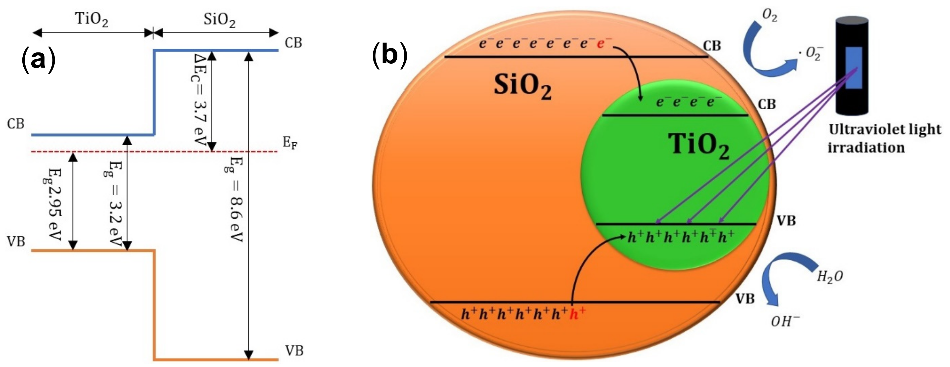
3.8. Photocatalytic Mechanism

Figure 10a shows a band diagram illustrating the energy levels of the conduction and valence bands for TiO2 and SiO2. It is important to point out that the conduction band energy of TiO2 is lower than that of SiO2; therefore, photo-excited electrons on both semiconductor layers are readily transferred to the conduction band of TiO2. Inspection of the energy band positions and scheme in Fig 10 also shows that photo-generated holes are promoted to the valence band of TiO2 where interphasial oxidation reactions may occur (in Figure 10b this hole-induced oxidation mechanism for methylene blue (MB) is depicted).
In this way, when the photocatalyst absorbs a photon with energy equal to or greater than the band gap energy, the photogenerated electrons and holes are efficiently separated by the space-charge layer, with the holes being transported to the TiO2 surface. The primary photon energy-derived elements that interact with H2O or OH- adsorbed on the surface to make ·OH are called photogenerated holes [50,51,52]. As can be seen from Figure 10b and the equations that follow:
TiO 2 + h ν h + + e
h + + H 2 O · OH + H +
h + + OH · OH
The superoxide radicals (·O2), which are highly oxidant species, are created when the photogenerated electrons interact with the O2 on the surface. In fact, these reactions produce a variety of active free radicals with high oxidizing characteristics, such as (·OH, ·O2, and HOO·). It should be highlighted, too, that the high rate of photogenerated e h+ recombination makes less effective photodegradation of challenging contaminants. According to [53,54], the interaction between TiO2 and SiO2 improves the separation of charge carriers (e and h+) and makes it easier for them to transfer between one another. As a result, the suppression of electron-hole recombination is only partially effective, leading to an increase in photoactivity.

4. Conclusions

The TiO2-SiO2 thin films’ structural, optical, and photocatalytic properties are synthesized and evaluated in this work, as well as the significance and importance of TiO2 modified SiO2 substrates. It has been demonstrated that TiO2-SiO2 thin films have high photocatalytic performance for the discoloration of Methylene Blue solutions, and likely for many diverse types of organic contaminants in aqueous effluents. The presence of the TiO2 layers on top of SiO2 thin films improved the photocatalytic properties of the films, due to the photo-generated electrons gathered in the TiO2 conduction band and were drawn to the SiO2 trap level, which inhibited the recombination of electrons and holes. The presence of nine layers of TiO2 in the surface of SiO2 yielded superior photocatalytic activity to the other samples. In the end, effective degradation of the model dye was achieved, which is crucial for the detoxification of water. In the future, by further controlling nanocrystals sizes and layers and mesopore sizes precisely, we can expect enhanced photocatalytic properties.

Author Contributions

Y.d.J.A.-S.: Conceived and designed the experiments, Research, Writing—original draft. M.T.-A.: Analyzed and interpreted the data, analysis tools or data. S.G.-H.: Research, proofreading. L.A.G.: Proofreading, Supervision. A.M.-L.: Conceptualization, Research, Supervision, Proofreading and editing. All authors have read and agreed to the published version of the manuscript.

Funding

This research received no external funding.

Data Availability Statement

The datasets used and/or analyzed during the current study are available from the corresponding author on reasonable request.

Acknowledgments

The authors would like to thank all members of the NanoBiotechnology and Photocatalysis Laboratory at Airport Campus of the Autonomous University of Querétaro.

Conflicts of Interest

The authors declare that they have no known competing financial interests or personal relationships that could have appeared to influence the work reported in this paper.

References

  1. Vaiano, V.; Sacco, O.; Sannino, D.; Ciambelli, P. Nanostructured N-doped TiO2 coated on glass spheres for the photocatalytic removal of organic dyes under UV or visible light irradiation. Appl. Catal. B 2015, 170, 153–161. [Google Scholar] [CrossRef]
  2. Bayomie, O.S.; Kandeel, H.; Shoeib, T.; Yang, H.; Youssef, N.; El-Sayed, M.M.H. Novel approach for effective removal of methylene blue dye from water using fava bean peel waste. Sci. Rep. 2020, 10, 7824. [Google Scholar] [CrossRef] [PubMed]
  3. Guidolin, T.O.; Possolli, N.M.; Polla, M.B.; Wermuth, T.B.; de Oliveira, T.F.; Eller, S.; Montedo, O.R.K.; Arcaro, S.; Cechinel, M.A.P. Photocatalytic pathway on the degradation of methylene blue from aqueous solutions using magnetite nanoparticles. J. Clean. Prod. 2021, 318, 128556. [Google Scholar]
  4. Ladole, M.R.; Pokale, P.B.; Patil, S.S.; Belokar, P.G.; Pandit, A.B. Laccase immobilized peroxidase mimicking magnetic metal organic frameworks for industrial dye degradation. Bioresour. Technol. 2020, 317, 124035. [Google Scholar] [CrossRef] [PubMed]
  5. Fu, Y.; Wang, L.; Peng, W.; Fan, Q.; Li, Q.; Dong, Y.; Liu, Y.; Boczkaj, G.; Wang, Z. Enabling simultaneous redox transformation of toxic chromium(VI) and arsenic (III) in aqueous media—A review. J. Hazard. Mater. 2021, 417, 126041. [Google Scholar] [CrossRef] [PubMed]
  6. Landge, V.K.; Sonawane, S.H.; Sivakumar, M.; Sonawane, S.S.; Babu, G.U.B.; Boczkaj, G. S-scheme heterojunction Bi2O3-ZnO/Bentonite clay composite with enhanced photocatalytic performance. Sustain. Energy Technol. Assess. 2021, 45, 101194. [Google Scholar] [CrossRef]
  7. Rayaroth, M.P.; Aravindakumar, C.T.; Shah, N.S.; Boczkaj, G. Advanced oxidation processes (AOPs) based wastewater treatment—Unexpected nitration side reactions—A serious environmental issue: A review. Chem. Eng. J. 2022, 430, 133002. [Google Scholar] [CrossRef]
  8. Chen, D.; Cheng, Y.; Zhou, N.; Chen, P.; Wang, Y.; Li, K.; Huo, S.; Cheng, P.; Peng, P.; Zhang, R.; et al. Photocatalytic degradation of organic pollutants using TiO2-based photocatalysts: A review. J. Clean. Prod. 2020, 268, 121725. [Google Scholar] [CrossRef]
  9. Radha, E.; Komaraiah, D.; Sayanna, R.; Sivakuma, J. Photoluminescence and photocatalytic activity of rare earth ions doped anatase TiO2 thin films. J. Lumin. 2022, 244, 118727. [Google Scholar] [CrossRef]
  10. Fouzia, A.; Rabah, B. The influence of doping lead and annealing temperature on grown of nanostructures of TiO2 thin films prepared by a sol-gel method. Mater. Sci. Eng. B 2021, 265, 114982. [Google Scholar] [CrossRef]
  11. Kamarulzaman, U.A.; Rahman, M.Y.A.; Su’ait, M.S.; Umar, A.A. Effect of annealing treatment on multilayer TiO2 films on the performance of dye-sensitized solar cells. Optik 2020, 218, 164976. [Google Scholar] [CrossRef]
  12. Lukong, V.T.; Ukoba, K.; Yoro, K.O.; Jen, T.C. Annealing temperature variation and its influence on the self-cleaning properties of TiO2 thin films. Heliyon 2022, 8, e09460. [Google Scholar] [CrossRef]
  13. Garlisi, C.; Palmisano, G. Radiation-free superhydrophilic and antifogging properties of e-beam evaporated TiO2 films on glass. Appl. Surf. Sci. 2017, 420, 83–93. [Google Scholar] [CrossRef]
  14. Rajput, R.B.; Jamble, S.N.; Kale, R.B. A review on TiO2/SnO2 heterostructures as a photocatalyst for the degradation of dyes and organic pollutants. J. Environ. Manag. 2022, 307, 114533. [Google Scholar] [CrossRef]
  15. Zhou, L.; Yan, S.; Tian, B.; Zhang, J.; Anpo, M. Preparation of TiO2–SiO2 film with high photocatalytic activity on PET substrate. Mater. Lett. 2006, 60, 396. [Google Scholar] [CrossRef]
  16. Ennaoui, A.; Sankapal, B.R.; Skryshevsky, V.; Lux-Steiner, M.C. TiO2 and TiO2–SiO2 thin films and powders by one-step soft-solution method: Synthesis and characterizations. Sol. Energy Mater. Sol. Cells 2006, 90, 1533–1541. [Google Scholar] [CrossRef]
  17. Chang, W.; Yan, L.; Liu, B.; Sun, R. Photocatalyic activity of double pore structure TiO2/SiO2 monoliths. Ceram. Int. 2017, 43, 5881–5886. [Google Scholar] [CrossRef]
  18. Ghosh, T.B.; Dhabal, S.; Datta, A.K. On crystallite size dependence of phase stability of nano-crystalline TiO2. J. Appl. Phys. 2003, 94, 4577–4582. [Google Scholar] [CrossRef]
  19. Zhang, J.; Huang, Z.; Xu, Y.; Kang, F. Carbon-coated TiO2 composites for the photocatalytic degradation of low concentration benzene. New Carbon Mater. 2011, 26, 63–70. [Google Scholar] [CrossRef]
  20. Torchynska, T.V.; Vazquez, A.L.Q.; Polupan, G.; Matsumoto, Y.; Khomenkova, L.; Shcherbyna, L. Correlation between the photoluminescence and different types of Si nano-clusters in amorphous silicon. J. Non-Cryst. Solids 2008, 354, 2186–2189. [Google Scholar] [CrossRef]
  21. Demirkol, U.; Pat, S.; Mohammadigharehbagh, R.; Musaoğlu, C.; Özgür, M.; Elmas, S.; Özen, S.; Korkmaz, Ş. Determination of the structural, morphological, and optical properties of graphene doped SnO thin films deposited by using thermionic vacuum arc technique. Phys. B Condens. Matter 2019, 569, 14–19. [Google Scholar] [CrossRef]
  22. Lin, S.S.; Huang, J.L. Effect of thickness on the structural and optical properties of ZnO films by r.f. magnetron sputtering. Surf. Coat. Technol. 2004, 185, 222–227. [Google Scholar] [CrossRef]
  23. Khan, M.I.; Imran, S.; Shahnawaz, D.; Saleem, M.; Rehman, S.U. Annealing effect on the structural, morphological, and electrical properties of TiO2/ZnO bilayer thin films. Results Phys. 2018, 8, 249–252. [Google Scholar] [CrossRef]
  24. Miled, I.B.; Jlassi, M.; Sta, I.; Dhaouadi, M.; Hajji, M.; Mousdis, G.; Kompitsas, M.; Ezzaouia, H. Influence of In-doping on microstructure, optical and electrical properties of sol–gel derived CdO thin films. J. Mater. Sci. Mater. Electron. 2018, 29, 11286–11295. [Google Scholar] [CrossRef]
  25. Away, R.D.Y.; Takai-Yamashita, C.; Ban, T.; Ohya, Y. Photocatalytic properties of TiO2-SiO2 sandwich multilayer films prepared by sol-gel dip-coating. Thin Solid Film. 2021, 720, 138522. [Google Scholar] [CrossRef]
  26. Kaveh, R.; Mokhtarifar, M.; Bagherzadeh, M.; Lucotti, A.; Diamanti, M.V.; Pedeferri, M. Magnetically Recoverable TiO2/SiO2/γ-Fe2O3/rGO Composite with Significantly Enhanced UV-Visible Light Photocatalytic Activity. Molecules 2020, 25, 2996. [Google Scholar] [CrossRef]
  27. Hao, B.; Guo, J.; Zhang, L.; Ma, H. Magnetron sputtered TiO2/CuO heterojunction thin films for efficient photocatalysis of Rhodamine B. J. Alloy. Compd. 2022, 903, 163851. [Google Scholar] [CrossRef]
  28. Amano, F.; Nakata, M.; Yamamoto, A.; Tanaka, T. Rutile titanium dioxide prepared by hydrogen reduction of Degussa P25 for highly efficient photocatalytic hydrogen evolution. Catal. Sci. Technol. 2016, 6, 5693–5699. [Google Scholar] [CrossRef]
  29. Xie, W.; Li, R.; Xu, Q. Enhanced photocatalytic activity of Se-doped TiO2 under visible light irradiation. Sci. Rep. 2018, 8, 8752. [Google Scholar] [CrossRef]
  30. Khan, M.I.; Bhatti, K.A.; Qindeel, R.; Althobaiti, H.S.; Alonizan, N. Structural, electrical and optical properties of multilayer TiO2 thin films deposited by sol–gel spin coating. Results Phys. 2017, 7, 1437–1439. [Google Scholar] [CrossRef]
  31. Fakhrutdinova, E.D.; Shabalina, A.V.; Gerasimova, M.A.; Nemoykina, A.L.; Vodyankina, O.V.; Svetlichnyi, V.A. Highly Defective Dark Nano Titanium Dioxide: Preparation via Pulsed Laser Ablation and Application. Materials 2020, 13, 2054. [Google Scholar] [CrossRef] [PubMed]
  32. Martínez, H.; Cáceres, M.F.; Martínez, F.; Páez-Mozo, E.A.; Valangec, S.; Castellanos, N.J.; Molina, D.; Barrault, J.; Arzoumanian, H. Photo-epoxidation of cyclohexene, cyclooctene and 1-octene with molecular oxygen catalyzed by dichloro dioxo-(4,4′-dicarboxylato-2,2′-bipyridine) molybdenum(VI) grafted on mesoporous TiO2. J. Mol. Catal. A Chem. 2016, 423, 248–255. [Google Scholar] [CrossRef]
  33. Frank, O.; Zukalova, M.; Laskova, B.; Kürti, J.; Koltai, J.; Kavan, L. Raman spectra of titanium dioxide (anatase, rutile) with identified oxygen isotopes (16, 17, 18). Phys. Chem. Chem. Phys. 2012, 14, 14567–14572. [Google Scholar] [CrossRef]
  34. Ekoi, E.J.; Gowen, A.; Dorrepaal, R.; Dowling, D.P. Characterisation of titanium oxide layers using Raman spectroscopy and optical profilometry: Influence of oxide properties. Results Phys. 2019, 12, 1574–1585. [Google Scholar] [CrossRef]
  35. Porto, S.P.S.; Fleury, P.A.; Damen, T.C. Raman Spectra of TiO2, MgF2, ZnF2, FeF2, MnF2. Phys. Rev. 1967, 154, 522–526. [Google Scholar] [CrossRef]
  36. Tompsett, G.A.; Bowmaker, G.A.; Cooney, R.P.; Metson, J.B.; Rodgers, K.A.; Seakins, J.M. The Raman spectrum of brookite, TiO2 (Pbca, Z = 8). J. Raman Spectrosc. 1995, 26, 57–62. [Google Scholar] [CrossRef]
  37. Stathatos, E.; Lianos, P.; DelMonte, F.; Levy, D.; Tsiourvas, D. Formation of TiO2 Nanoparticles in Reverse Micelles and Their Deposition as Thin Films on Glass Substrates. Langmuir 1997, 13, 4295–4300. [Google Scholar] [CrossRef]
  38. Yu, J.C.; Yu, J.; Zhao, J. Enhanced photocatalytic activity of mesoporous and ordinary TiO2 thin films by sulfuric acid treatment. Appl. Catal. B Environ. 2002, 36, 31–43. [Google Scholar] [CrossRef]
  39. Stathatos, E.; Lianos, P.; Falaras, P.; Siokou, A. Photocatalytically Deposited Silver Nanoparticles on Mesoporous TiO2 Films. Langmuir 2000, 16, 2398–2400. [Google Scholar] [CrossRef]
  40. Haapanen, J.; Aromaa, M.; Teisala, H.; Tuominen, M.; Stepien, M.; Saarinen, J.J.; Heikkila, M.; Toivakka, M.; Kuusipalo, J.; Makela, J.M. Binary TiO2/SiO2 nanoparticle coating for controlling the wetting properties of paperboard. Mater. Chem. Phys. 2015, 149–150, 230–237. [Google Scholar] [CrossRef]
  41. Yu, B.; Leung, K.M.; Guo, Q.; Lau, W.M.; Yang, J. Synthesis of Ag-TiO2 composite nano thin film for antimicrobial application. Nanotechnology 2011, 22, 115603. [Google Scholar] [CrossRef]
  42. Pelaez, M.; Nolan, N.T.; Pillai, S.C.; Seery, M.K.; Falaras, P.; Kontos, A.G.; Dunlop, P.S.M.; Hamilton, J.W.J.; Byrne, J.A.; O’Shea, K.; et al. A review on the visible light active titanium dioxide photocatalysts for environmental applications. Appl. Catal. B Environ. 2012, 125, 331–349. [Google Scholar] [CrossRef]
  43. Suzuki, N.; Jiang, X.; Radhakrishnan, L.; Takai, K.; Shimasaki, K.; Huang, Y.-T.; Miyamoto, N.; Yamauchi, Y. Hybridization of Photoactive Titania Nanoparticles with Mesoporous Silica Nanoparticles and Investigation of Their Photocatalytic Activity. Bull. Chem. Soc. Jpn. 2011, 84, 812–817. [Google Scholar] [CrossRef]
  44. Zhang, Z.; Wang, C.; Zakaria, R.; Ying, J. Role of Particle Size in Nanocrystalline TiO2-Based Photocatalysts. J. Phys. Chem. B 1998, 102, 10871–10878. [Google Scholar] [CrossRef]
  45. Afshar, S.; Jahromi, H.S.; Jafari, N.; Ahmadi, Z.; Hakamizadeh, M. Degradation of malachite green oxalate by UV and visible lights irradiation using Pt/TiO2/SiO2 nanophotocatalyst. Sci. Iran. 2011, 18, 772–779. [Google Scholar] [CrossRef]
  46. Al-Ekabi, H.; Serpone, N. Kinetic studies in heterogeneous photocatalysis. 1. Photocatalytic degradation of chlorinated phenols in aerated aqueous solution over TiO2 supported on glass matrix. J. Phys. Chem. 1988, 92, 5726–5731. [Google Scholar] [CrossRef]
  47. Yadav, H.M.; Kim, J.S. Fabrication of SiO2/TiO2 double layer thin films with self- cleaning and photocatalytic properties. J. Mater. Sci. Mater. Electron. 2016, 27, 10082–10088. [Google Scholar] [CrossRef]
  48. Fu, X.; Clark, L.A.; Yang, Q.; Anderson, M.A. Enhanced photocatalytic performance of titania-based binary metal oxides: TiO2/SiO2 and TiO2/ZrO2. Environ. Sci. Technol. 1996, 30, 647–653. [Google Scholar] [CrossRef]
  49. Lu, J.; Kosuda, M.; Van Duyne, R.P.; Stair, P.C. Surface acidity and properties of TiO2/SiO2 catalysts prepared by atomic layer deposition: UV-visible diffuse reflectance, DRIFTS, and visible Raman spectroscopy. J. Phys. Chem. C 2009, 113, 12412–12418. [Google Scholar] [CrossRef]
  50. Gao, R.Q.; Sun, Q.; Fang, Z.; Li, G.T.; Jia, M.Z.; Hou, X.M. Preparation of nano-TiO2/diatomite-based porous ceramics and their photocatalytic kinetics for formaldehyde degradation. Int. J. Miner. Metall. Mater. 2018, 25, 73–79. [Google Scholar] [CrossRef]
  51. Gnanaprakasam, A.; Sivakumar, V.M.; Sivayogavalli, P.L.; Thirumarimurugan, M. Characterization of TiO2 and ZnO nanoparticles and their applications in photocatalytic degradation of azodyes. Ecotoxicol. Environ. Saf. 2015, 121, 121–125. [Google Scholar] [CrossRef] [PubMed]
  52. Guo, Q.; Zhou, C.; Ma, Z.; Yang, X. Fundamentals of TiO2 Photocatalysis: Concepts, Mechanisms, and Challenges. Adv. Mater. 2019, 31, e1901997. [Google Scholar] [CrossRef] [PubMed]
  53. Nabih, S.; Shalan, A.E.; Serea, E.S.A.; Goda, M.A.; Sanad, M.F. Photocatalytic performance of TiO2@SiO2 nanocomposites for the treatment of different organic dyes. J. Mater. Sci. Mater. Electron. 2019, 30, 9623–9633. [Google Scholar] [CrossRef]
  54. Gholami, T.; Bazarganipour, M.; Salavati-Niasari, M.; Bagheri, S. Photocatalytic degradation of methylene blue on TiO2@SiO2 core/shell nanoparticles: Synthesis and characterization. J. Mater. Sci. Mater. Electron. 2015, 26, 6170–6177. [Google Scholar] [CrossRef]
Figure 1. (a) Sequential steps of the sol–gel dip-coating method for thin film deposition. (b) Dip coating system assembled in the NanoBiotechnology and Photocatalysis Laboratory—UAQ. This system is used for the production of various thin films.
Nanomaterials 13 01403 g001
Figure 2. X-ray diffraction patterns for samples of TiO2 over SiO2 annealed. The tetragonal phase is linked to thin films of TiO2 that correspond to the (hkl) indices.
Nanomaterials 13 01403 g002
Figure 3. Crystallite size and strain of TiO2-SiO2 thin films based on the quantity of dip-coating layers.
Nanomaterials 13 01403 g003
Figure 4. Determination of E g energy for TiO2-SiO2 thin films. (ac) Spectral dependence of T(λ) and R(λ) coefficients, (d) UV–Visible reflectance spectra of TiO2-SiO2 thin films, (e) E g determined by optical method using (αhν)1/2 vs. hν plots of thin films deposited with different numbers of TiO2-SiO2 layers.
Nanomaterials 13 01403 g004
Figure 5. Raman spectrum of TiO2-SiO2 thin films heated to 550 °C in air (anatase).
Nanomaterials 13 01403 g005
Figure 6. 2- and 3-dimensional images of TiO2-SiO2 thin films with different numbers of layers. (a) 5TiO2-9SiO2 (5 layers), (b) 7TiO2-9SiO2 (7 layers), and (c) 9TiO2-9SiO2 (9 layers).
Nanomaterials 13 01403 g006
Figure 7. SEM pictures of: (a) sample 5TiO2-9SiO2; (b) sample 7TiO2-9SiO2; (c) sample 9TiO2-9SiO2.
Nanomaterials 13 01403 g007
Figure 8. TEM micrography of sample 7TiO2-9SiO2 (a) Size distribution of 7TiO2-9SiO2 nanoparticles on thin films. (b) The disordered wormhole-like pore structure, (ce) High-resolution TEM micrograph of 7TiO2-9SiO2 thin films; crystalline planes are observed. This Figure shows the inter-planar distance obtained from various zones of the sample. (f) SAED pattern of 7TiO2-9SiO2 thin films indexed using anatase TiO2 crystallographic parameters.
Nanomaterials 13 01403 g008
Figure 9. (a) Normalized concentration of MB vs UV-light irradiation time in the presence of TiO2-SiO2 thin films. (b) Reaction kinetics of MB photocatalytic degradation at different loadings of TiO2-SiO2 catalyst.
Nanomaterials 13 01403 g009
Figure 10. (a) TiO2-SiO2 Band diagram. ∆CB and ∆VB denote the conduction and valence band offset between SiO2 and TiO2, respectively, and EF denote the Fermi level. (b) Photodegradation mechanism of TiO2-SiO2 under UV light irradiation.
Nanomaterials 13 01403 g010
Table 1. Results of the photodegradation of MB.
Sample k (h−1) R2Degradation (%)
9SiO20.0480.99721
9TiO20.4060.98282
5TiO2-9SiO20.3970.98283
7TiO2-9SiO20.4980.95689
9TiO2-9SiO20.9780.99398
Disclaimer/Publisher’s Note: The statements, opinions and data contained in all publications are solely those of the individual author(s) and contributor(s) and not of MDPI and/or the editor(s). MDPI and/or the editor(s) disclaim responsibility for any injury to people or property resulting from any ideas, methods, instructions or products referred to in the content.

