
Noble-Metal Nanoparticle-Embedded Silicon Nanogratings via Single-Step Laser-Induced Periodic Surface Structuring
 , , , and
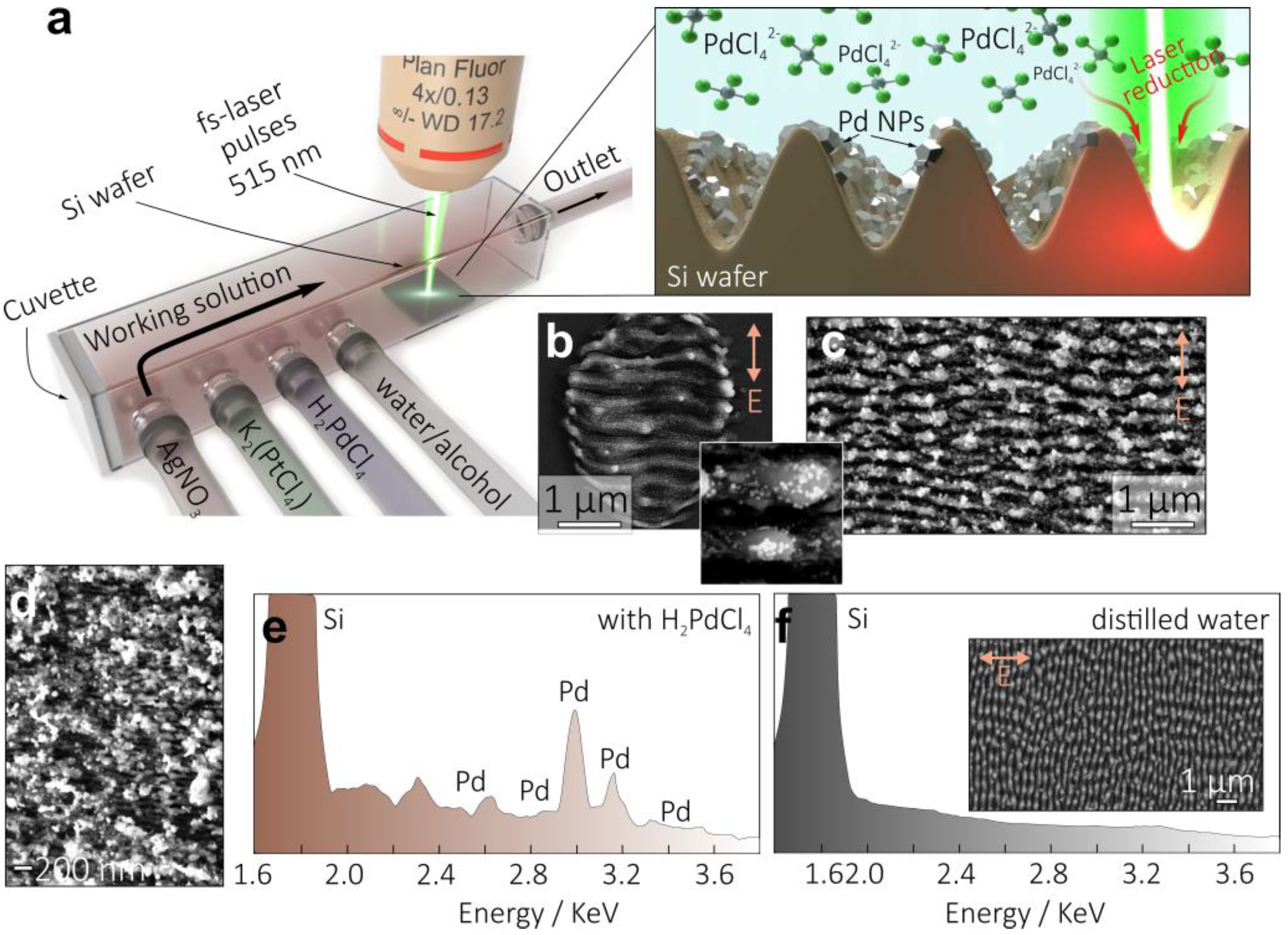
Abstract
:1. Introduction
2. Materials and Methods
2.1. Materials
2.2. Laser-Assisted Fabrication of Nanoparticle-Decorated Si Nanogratings
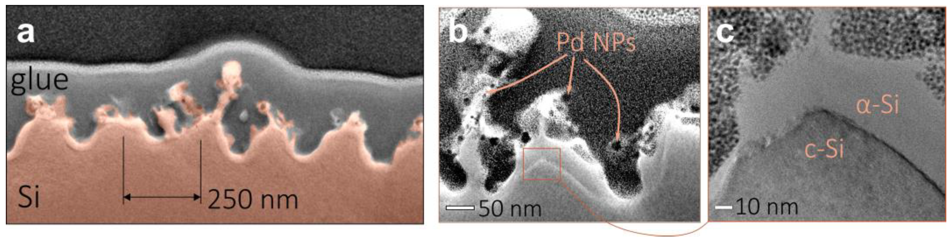
2.3. Structural Characterization of Nanoparticle-Decorated Si Nanogratings
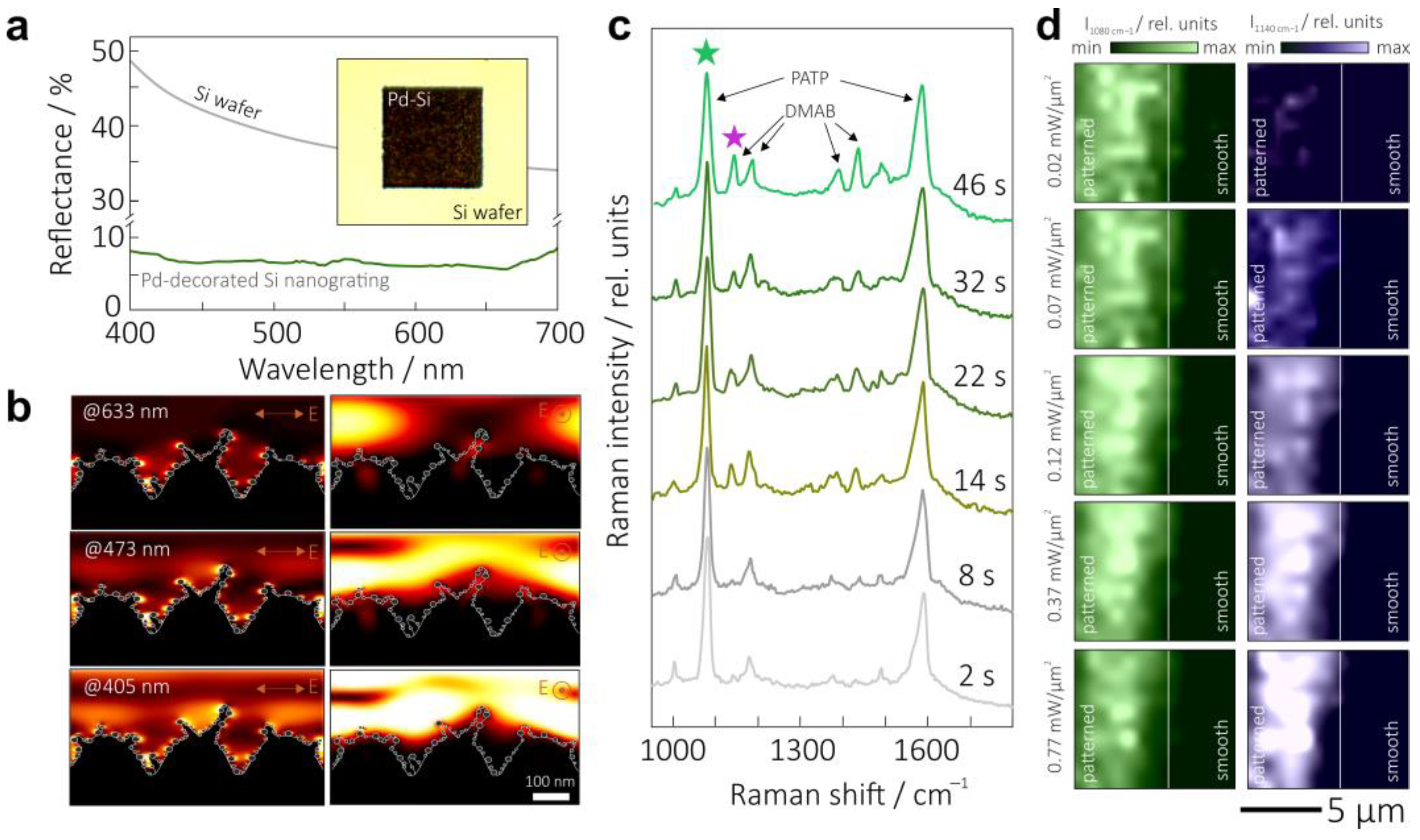
2.4. Optical and Raman Characterization of Nanoparticle-Decorated Si Nanogratings
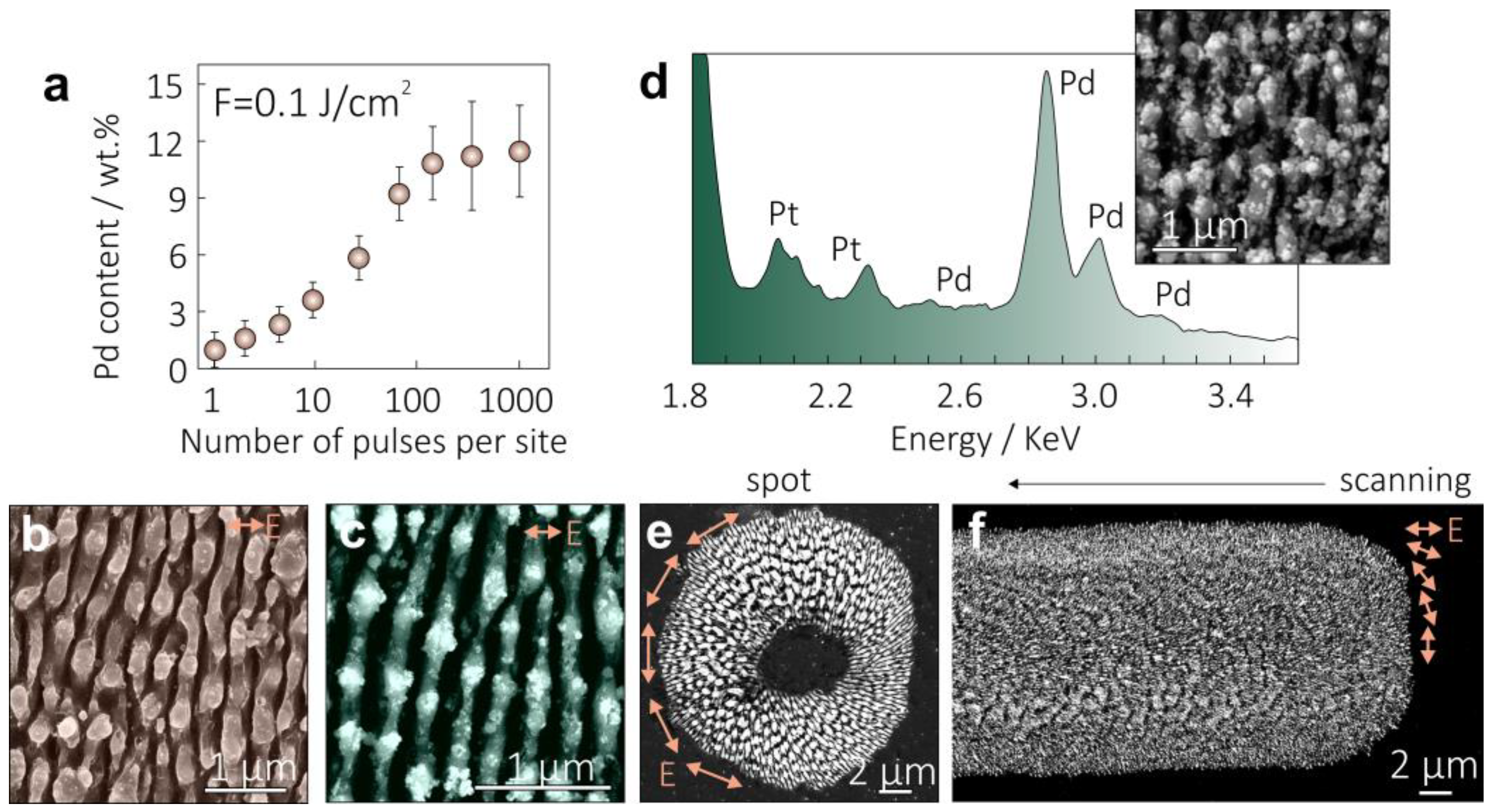
3. Results
4. Conclusions
Author Contributions
Funding
Data Availability Statement
Conflicts of Interest
References
- Campelo, J.M.; Luna, D.; Luque, R.; Marinas, J.M.; Romero, A.A. Sustainable Preparation of Supported Metal Nanoparticles and Their Applications in Catalysis. ChemSusChem 2009, 2, 18–45. [Google Scholar] [CrossRef]
- Astruc, D.; Lu, F.; Aranzaes, J.R. Nanoparticles as Recyclable Catalysts: The Frontier between Homogeneous and Heterogeneous Catalysis. Angew. Chemie Int. Ed. 2005, 44, 7852–7872. [Google Scholar] [CrossRef]
- Narayanan, R.; El-Sayed, M.A. Catalysis with Transition Metal Nanoparticles in Colloidal Solution: Nanoparticle Shape Dependence and Stability. J. Phys. Chem. B 2005, 109, 12663–12676. [Google Scholar] [CrossRef]
- Ilunga, A.K.; Meijboom, R. Catalytic Oxidation of Methylene Blue by Dendrimer Encapsulated Silver and Gold Nanoparticles. J. Mol. Catal. A Chem. 2016, 411, 48–60. [Google Scholar] [CrossRef]
- Chen, S.; Kucernak, A. Electrocatalysis under Conditions of High Mass Transport Rate: Oxygen Reduction on Single Submicrometer-Sized Pt Particles Supported on Carbon. J. Phys. Chem. B 2004, 108, 3262–3276. [Google Scholar] [CrossRef]
- Claus, P.; Hofmeister, H. Electron Microscopy and Catalytic Study of Silver Catalysts: Structure Sensitivity of the Hydrogenation of Crotonaldehyde. J. Phys. Chem. B 1999, 103, 2766–2775. [Google Scholar] [CrossRef]
- Gilroy, K.D.; Ruditskiy, A.; Peng, H.-C.; Qin, D.; Xia, Y. Bimetallic Nanocrystals: Syntheses, Properties, and Applications. Chem. Rev. 2016, 116, 10414–10472. [Google Scholar] [CrossRef]
- Mitsai, E.; Kuchmizhak, A.; Pustovalov, E.; Sergeev, A.; Mironenko, A.; Bratskaya, S.; Linklater, D.P.P.; Balčytis, A.; Ivanova, E.; Juodkazis, S. Chemically Non-Perturbing SERS Detection of a Catalytic Reaction with Black Silicon. Nanoscale 2018, 10, 9780–9787. [Google Scholar] [CrossRef] [Green Version]
- Schauermann, S.; Nilius, N.; Shaikhutdinov, S.; Freund, H.-J. Nanoparticles for Heterogeneous Catalysis: New Mechanistic Insights. Acc. Chem. Res. 2013, 46, 1673–1681. [Google Scholar] [CrossRef]
- Hansen, T.W.; DeLaRiva, A.T.; Challa, S.R.; Datye, A.K. Sintering of Catalytic Nanoparticles: Particle Migration or Ostwald Ripening? Acc. Chem. Res. 2013, 46, 1720–1730. [Google Scholar] [CrossRef]
- Cuenya, B.R. Synthesis and Catalytic Properties of Metal Nanoparticles: Size, Shape, Support, Composition, and Oxidation State Effects. Thin Solid Films 2010, 518, 3127–3150. [Google Scholar] [CrossRef]
- Xu, D.; Lv, H.; Liu, B. Encapsulation of Metal Nanoparticle Catalysts Within Mesoporous Zeolites and Their Enhanced Catalytic Performances: A Review. Front. Chem. 2018, 6, 550. [Google Scholar] [CrossRef] [PubMed]
- Liu, B.; Kuo, C.-H.; Chen, J.; Luo, Z.; Thanneeru, S.; Li, W.; Song, W.; Biswas, S.; Suib, S.L.; He, J. Ligand-Assisted Co-Assembly Approach toward Mesoporous Hybrid Catalysts of Transition-Metal Oxides and Noble Metals: Photochemical Water Splitting. Angew. Chemie Int. Ed. 2015, 54, 9061–9065. [Google Scholar] [CrossRef] [PubMed]
- Liu, B.; Wang, P.; Lopes, A.; Jin, L.; Zhong, W.; Pei, Y.; Suib, S.L.; He, J. Au–Carbon Electronic Interaction Mediated Selective Oxidation of Styrene. ACS Catal. 2017, 7, 3483–3488. [Google Scholar] [CrossRef]
- Avramenko, V.A.; Bratskaya, S.Y.; Karpov, P.A.; Mayorov, V.Y.; Mironenko, A.Y.; Palamarchuk, M.S.; Sergienko, V.I. Macroporous Catalysts for Liquid-Phase Oxidation on the Basis of Manganese Oxides Containing Gold Nanoparticles. Dokl. Phys. Chem. 2010, 435, 193–197. [Google Scholar] [CrossRef]
- Borodaenko, Y.; Syubaev, S.; Khairullina, E.; Tumkin, I.; Gurbatov, S.; Mironenko, A.; Mitsai, E.; Zhizhchenko, A.; Modin, E.; Gurevich, E.L.; et al. On-Demand Plasmon Nanoparticle-Embedded Laser-Induced Periodic Surface Structures (LIPSSs) on Silicon for Optical Nanosensing. Adv. Opt. Mater. 2022, 10, 2201094. [Google Scholar] [CrossRef]
- Sun, X.; Li, Y. Colloidal Carbon Spheres and Their Core/Shell Structures with Noble-Metal Nanoparticles. Angew. Chemie 2004, 116, 607–611. [Google Scholar] [CrossRef]
- Mironenko, A.Y.; Sergeev, A.A.; Nazirov, A.E.; Modin, E.B.; Voznesenskiy, S.S.; Bratskaya, S.Y. H2S Optical Waveguide Gas Sensors Based on Chitosan/Au and Chitosan/Ag Nanocomposites. Sens. Actuators B Chem. 2016, 225, 348–353. [Google Scholar] [CrossRef]
- Pestov, A.; Nazirov, A.; Modin, E.; Mironenko, A.; Bratskaya, S. Mechanism of Au(III) Reduction by Chitosan: Comprehensive Study with 13C and 1H NMR Analysis of Chitosan Degradation Products. Carbohydr. Polym. 2015, 117, 70–77. [Google Scholar] [CrossRef]
- Mironenko, A.; Modin, E.; Sergeev, A.; Voznesenskiy, S.; Bratskaya, S. Fabrication and Optical Properties of Chitosan/Ag Nanoparticles Thin Film Composites. Chem. Eng. J. 2014, 244, 457–463. [Google Scholar] [CrossRef]
- Borodaenko, Y.; Gurbatov, S.; Tutov, M.; Zhizhchenko, A.; Kulinich, S.A.; Kuchmizhak, A.; Mironenko, A. Direct Femtosecond Laser Fabrication of Chemically Functionalized Ultra-Black Textures on Silicon for Sensing Applications. Nanomaterials 2021, 11, 401. [Google Scholar] [CrossRef] [PubMed]
- Dostovalov, A.; Bronnikov, K.; Korolkov, V.; Babin, S.; Mitsai, E.; Mironenko, A.; Tutov, M.; Zhang, D.; Sugioka, K.; Maksimovic, J.; et al. Hierarchical Anti-Reflective Laser-Induced Periodic Surface Structures (LIPSSs) on Amorphous Si Films for Sensing Applications. Nanoscale 2020, 12, 13431–13441. [Google Scholar] [CrossRef]
- Pavliuk, G.; Pavlov, D.; Mitsai, E.; Vitrik, O.; Mironenko, A.; Zakharenko, A.; Kulinich, S.A.; Juodkazis, S.; Bratskaya, S.; Zhizhchenko, A.; et al. Ultrasensitive SERS-Based Plasmonic Sensor with Analyte Enrichment System Produced by Direct Laser Writing. Nanomaterials 2019, 10, 49. [Google Scholar] [CrossRef] [PubMed] [Green Version]
- Mironenko, A.Y.; Tutov, M.V.; Sergeev, A.A.; Mitsai, E.V.; Ustinov, A.Y.; Zhizhchenko, A.Y.; Linklater, D.P.; Bratskaya, S.Y.; Juodkazis, S.; Kuchmizhak, A.A. Ultratrace Nitroaromatic Vapor Detection via Surface-Enhanced Fluorescence on Carbazole-Terminated Black Silicon. ACS Sens. 2019, 4, 2879–2884. [Google Scholar] [CrossRef]
- Mitsai, E.; Naffouti, M.; David, T.; Abbarchi, M.; Hassayoun, L.; Storozhenko, D.; Mironenko, A.; Bratskaya, S.; Juodkazis, S.; Makarov, S.; et al. Si 1−x Ge x Nanoantennas with a Tailored Raman Response and Light-to-Heat Conversion for Advanced Sensing Applications. Nanoscale 2019, 11, 11634–11641. [Google Scholar] [CrossRef]
- Bonse, J.; Krüger, J.; Höhm, S.; Rosenfeld, A. Femtosecond Laser-Induced Periodic Surface Structures. J. Laser Appl. 2012, 24, 042006. [Google Scholar] [CrossRef]
- Öktem, B.; Pavlov, I.; Ilday, S.; Kalaycıoğlu, H.; Rybak, A.; Yavaş, S.; Erdoğan, M.; Ilday, F.Ö. Nonlinear Laser Lithography for Indefinitely Large-Area Nanostructuring with Femtosecond Pulses. Nat. Photonics 2013, 7, 897–901. [Google Scholar] [CrossRef]
- Flamm, D.; Grossmann, D.G.; Sailer, M.; Kaiser, M.; Zimmermann, F.; Chen, K.; Jenne, M.; Kleiner, J.; Hellstern, J.; Tillkorn, C.; et al. Structured Light for Ultrafast Laser Micro- and Nanoprocessing. Opt. Eng. 2021, 60, 025105. [Google Scholar] [CrossRef]
- Stratakis, E.; Bonse, J.; Heitz, J.; Siegel, J.; Tsibidis, G.D.; Skoulas, E.; Papadopoulos, A.; Mimidis, A.; Joel, A.-C.; Comanns, P.; et al. Laser Engineering of Biomimetic Surfaces. Mater. Sci. Eng. R Rep. 2020, 141, 100562. [Google Scholar] [CrossRef]
- Papadopoulos, A.; Skoulas, E.; Mimidis, A.; Perrakis, G.; Kenanakis, G.; Tsibidis, G.D.; Stratakis, E. Biomimetic Omnidirectional Antireflective Glass via Direct Ultrafast Laser Nanostructuring. Adv. Mater. 2019, 31, 1901123. [Google Scholar] [CrossRef]
- Livakas, N.; Skoulas, E.; Stratakis, E. Omnidirectional Iridescence via Cylindrically- Polarized Femtosecond Laser Processing. Opto-Electron. Adv. 2020, 3, 190035. [Google Scholar] [CrossRef]
- Liu, M.; Li, M.-T.; Xu, S.; Yang, H.; Sun, H.-B. Bioinspired Superhydrophobic Surfaces via Laser-Structuring. Front. Chem. 2020, 8, 835. [Google Scholar] [CrossRef] [PubMed]
- Khatri, O.P.; Ichii, T.; Murase, K.; Sugimura, H. UV induced covalent assembly of gold nanoparticles in linear patterns on oxide free silicon surface. J. Mater. Chem. 2012, 22, 16546–16551. [Google Scholar] [CrossRef]
- Nguyen, C.M.; Frias Batista, L.M.; John, M.G.; Rodrigues, C.J.; Tibbetts, K.M. Mechanism of Gold–Silver Alloy Nanoparticle Formation by Laser Coreduction of Gold and Silver Ions in Solution. J. Phys. Chem. B 2021, 125, 907–917. [Google Scholar] [CrossRef] [PubMed]
- Nag, A.; Frias Batista, L.M.; Tibbetts, K.M. Synthesis of Air-Stable Cu Nanoparticles Using Laser Reduction in Liquid. Nanomaterials 2021, 11, 814. [Google Scholar] [CrossRef] [PubMed]
- Peng, Y.; Cao, J.; Sha, Y.; Yang, W.; Li, L.; Liu, Z. Laser Solid-Phase Synthesis of Single-Atom Catalysts. Light Sci. Appl. 2021, 10, 168. [Google Scholar] [CrossRef]
- Broadhead, E.J.; Tibbetts, K.M. Fabrication of Gold–Silicon Nanostructured Surfaces with Reactive Laser Ablation in Liquid. Langmuir 2020, 36, 10120–10129. [Google Scholar] [CrossRef] [PubMed]
- Lin, C.-H.; Jiang, L.; Chai, Y.-H.; Xiao, H.; Chen, S.-J.; Tsai, H.-L. One-Step Fabrication of Nanostructures by Femtosecond Laser for Surface-Enhanced Raman Scattering. Opt. Express 2009, 17, 21581. [Google Scholar] [CrossRef]
- Li, C.; Hu, J.; Jiang, L.; Xu, C.; Li, X.; Gao, Y.; Qu, L. Shaped Femtosecond Laser Induced Photoreduction for Highly Controllable Au Nanoparticles Based on Localized Field Enhancement and Their SERS Applications. Nanophotonics 2020, 9, 691–702. [Google Scholar] [CrossRef]
- Beresna, M.; Gecevičius, M.; Kazansky, P.G.; Gertus, T. Radially Polarized Optical Vortex Converter Created by Femtosecond Laser Nanostructuring of Glass. Appl. Phys. Lett. 2011, 98, 201101. [Google Scholar] [CrossRef]
- Borodaenko, Y.; Syubaev, S.; Gurbatov, S.; Zhizhchenko, A.; Porfirev, A.; Khonina, S.; Mitsai, E.; Gerasimenko, A.V.; Shevlyagin, A.; Modin, E.; et al. Deep Subwavelength Laser-Induced Periodic Surface Structures on Silicon as a Novel Multifunctional Biosensing Platform. ACS Appl. Mater. Interfaces 2021, 13, 54551–54560. [Google Scholar] [CrossRef]
- Bronnikov, K.; Dostovalov, A.; Cherepakhin, A.; Mitsai, E.; Nepomniaschiy, A.; Kulinich, S.A.; Zhizhchenko, A.; Kuchmizhak, A. Large-Scale and Localized Laser Crystallization of Optically Thick Amorphous Silicon Films by Near-IR Femtosecond Pulses. Materials 2020, 13, 5296. [Google Scholar] [CrossRef]
- Bonse, J. Quo Vadis LIPSS?—Recent and Future Trends on Laser-Induced Periodic Surface Structures. Nanomaterials 2020, 10, 1950. [Google Scholar] [CrossRef] [PubMed]
- Buividas, R.; Mikutis, M.; Juodkazis, S. Surface and Bulk Structuring of Materials by Ripples with Long and Short Laser Pulses: Recent Advances. Prog. Quantum Electron. 2014, 38, 119–156. [Google Scholar] [CrossRef]
- Gurevich, E.L.; Gurevich, S.V. Laser Induced Periodic Surface Structures Induced by Surface Plasmons Coupled via Roughness. Appl. Surf. Sci. 2014, 302, 118–123. [Google Scholar] [CrossRef] [Green Version]
- Sipe, J.E.; Young, J.F.; Preston, J.S.; van Driel, H.M. Laser-Induced Periodic Surface Structure. I. Theory. Phys. Rev. B 1983, 27, 1141–1154. [Google Scholar] [CrossRef]
- Gurevich, E.L.; Levy, Y.; Bulgakova, N.M. Three-Step Description of Single-Pulse Formation of Laser-Induced Periodic Surface Structures on Metals. Nanomaterials 2020, 10, 1836. [Google Scholar] [CrossRef]
- Baranauskaite, V.E.; Novomlinskii, M.O.; Tumkin, I.I.; Khairullina, E.M.; Mereshchenko, A.S.; Balova, I.A.; Panov, M.S.; Kochemirovsky, V.A. In Situ Laser-Induced Synthesis of Gas Sensing Microcomposites Based on Molybdenum and Its Oxides. Compos. Part B Eng. 2019, 157, 322–330. [Google Scholar] [CrossRef]
- Panov, M.S.; Khairullina, E.M.; Vshivtcev, F.S.; Ryazantsev, M.N.; Tumkin, I.I. Laser-Induced Synthesis of Composite Materials Based on Iridium, Gold and Platinum for Non-Enzymatic Glucose Sensing. Materials 2020, 13, 3359. [Google Scholar] [CrossRef] [PubMed]
- Khairullina, E.M.; Tumkin, I.I.; Stupin, D.D.; Smikhovskaia, A.V.; Mereshchenko, A.S.; Lihachev, A.I.; Vasin, A.V.; Ryazantsev, M.N.; Panov, M.S. Laser-Assisted Surface Modification of Ni Microstructures with Au and Pt toward Cell Biocompatibility and High Enzyme-Free Glucose Sensing. ACS Omega 2021, 6, 18099–18109. [Google Scholar] [CrossRef]
- Frias Batista, L.M.; Kunzler, K.; John, M.G.; Clark, B.; Bullock, A.; Ferri, J.; Gupton, B.F.; Tibbetts, K.M. Laser Synthesis of Uncapped Palladium Nanocatalysts. Appl. Surf. Sci. 2021, 557, 149811. [Google Scholar] [CrossRef]
- Fan, G.; Ren, S.; Qu, S.; Guo, Z.; Wang, Q.; Wang, Y.; Gao, R. Mechanisms for Fabrications and Nonlinear Optical Properties of Pd and Pt Nanoparticles by Femtosecond Laser. Opt. Commun. 2013, 295, 219–225. [Google Scholar] [CrossRef]
- Nakashima, N.; Yamanaka, K.; Saeki, M.; Ohba, H.; Taniguchi, S.; Yatsuhashi, T. Metal Ion Reductions by Femtosecond Laser Pulses with Micro-Joule Energy and Their Efficiencies. J. Photochem. Photobiol. A Chem. 2016, 319–320, 70–77. [Google Scholar] [CrossRef] [Green Version]
- Shanthi, K.; Vimala, K.; Gopi, D.; Kannan, S. Fabrication of a PH Responsive DOX Conjugated PEGylated Palladium Nanoparticle Mediated Drug Delivery System: An In Vitro and In Vivo Evaluation. RSC Adv. 2015, 5, 44998–45014. [Google Scholar] [CrossRef]
- Saeki, M.; Taguchi, T.; Nakashima, N.; Ohba, H. Wet Separation between Palladium(II) and Molybdenum(IV) Ions by Using Laser-Induced Particle Formation: Enhancement of Recovery Efficiency of Palladium by Laser Condition. J. Photochem. Photobiol. A Chem. 2015, 299, 189–193. [Google Scholar] [CrossRef]
- Quinson, J.; Kacenauskaite, L.; Schröder, J.; Simonsen, S.B.; Theil Kuhn, L.; Vosch, T.; Arenz, M. UV-Induced Syntheses of Surfactant-Free Precious Metal Nanoparticles in Alkaline Methanol and Ethanol. Nanoscale Adv. 2020, 2, 2288–2292. [Google Scholar] [CrossRef] [PubMed]
- Mehrabanian, M.; Morselli, D.; Caputo, G.; Scarpellini, A.; Palazon, F.; Athanassiou, A.; Fragouli, D. Laser-Induced in Situ Synthesis of Pd and Pt Nanoparticles on Polymer Films. Appl. Phys. A 2016, 122, 1075. [Google Scholar] [CrossRef]
- Saeki, M.; Matsumura, D.; Yomogida, T.; Taguchi, T.; Tsuji, T.; Saitoh, H.; Ohba, H. In Situ Time-Resolved XAFS Studies on Laser-Induced Particle Formation of Palladium Metal in an Aqueous/EtOH Solution. J. Phys. Chem. C 2019, 123, 817–824. [Google Scholar] [CrossRef]
- Li, F.; Shang, Y.; Ding, Z.; Weng, H.; Xiao, J.; Lin, M. Efficient Extraction and Separation of Palladium (Pd) and Ruthenium (Ru) from Simulated HLLW by Photoreduction. Sep. Purif. Technol. 2017, 182, 9–18. [Google Scholar] [CrossRef]
- Li, Z.; Di, M.; Wei, W.; Leng, L.; Li, Z.; He, C.; Tan, Q.; Xu, Q.; Horton, J.H.; Li, L.; et al. Alkali Ion-Promoted Palladium Subnanoclusters Stabilized on Porous Alumina Nanosheets with Enhanced Catalytic Activity for Benzene Oxidation. Nano Res. 2022, 15, 5912–5921. [Google Scholar] [CrossRef]
- Enneiymy, M.; Fioux, P.; Le Drian, C.; Matei Ghimbeu, C.; Becht, J.-M. Palladium Nanoparticles Embedded in Mesoporous Carbons as Efficient, Green and Reusable Catalysts for Mild Hydrogenations of Nitroarenes. RSC Adv. 2020, 10, 36741–36750. [Google Scholar] [CrossRef]
- Pérez, J.; Serrano, J.L.; Sánchez, G.; Lozano, P.; da Silva, I.; Alcolea, A. From Coordination Complexes to Potential Heterogeneous Catalysts via Solid-State Thermal Decomposition: Precursor, Atmosphere and Temperature as Tuning Variables. ChemistrySelect 2019, 4, 8365–8371. [Google Scholar] [CrossRef]
- Enneiymy, M.; Le Drian, C.; Matei Ghimbeu, C.; Becht, J.-M. Reusable Magnetic Pd x Co y Nanoalloys Confined in Mesoporous Carbons for Green Suzuki–Miyaura Reactions. RSC Adv. 2018, 8, 17176–17182. [Google Scholar] [CrossRef] [Green Version]
- Jóźwiak, W.K.; Maniecki, T.P. Influence of Atmosphere Kind on Temperature Programmed Decomposition of Noble Metal Chlorides. Thermochim. Acta 2005, 435, 151–161. [Google Scholar] [CrossRef]
- Skoulas, E.; Manousaki, A.; Fotakis, C.; Stratakis, E. Biomimetic Surface Structuring Using Cylindrical Vector Femtosecond Laser Beams. Sci. Rep. 2017, 7, 45114. [Google Scholar] [CrossRef] [Green Version]
- Wang, T.; Lin, L.; Zhang, N. Compound Structures of Periodic Holes and Curved Ripples Fabricated by the Interference between the Converging Surface Plasmon Polaritons and Femtosecond Laser. Appl. Sci. 2022, 12, 2543. [Google Scholar] [CrossRef]
- Maalouf, M.; Abou Khalil, A.; Di Maio, Y.; Papa, S.; Sedao, X.; Dalix, E.; Peyroche, S.; Guignandon, A.; Dumas, V. Polarization of Femtosecond Laser for Titanium Alloy Nanopatterning Influences Osteoblastic Differentiation. Nanomaterials 2022, 12, 1619. [Google Scholar] [CrossRef]
- Lou, K.; Qian, S.-X.; Wang, X.-L.; Li, Y.; Gu, B.; Tu, C.; Wang, H.-T. Two-Dimensional Microstructures Induced by Femtosecond Vector Light Fields on Silicon. Opt. Express 2012, 20, 120. [Google Scholar] [CrossRef] [PubMed]
- Huang, Y.-F.; Zhu, H.-P.; Liu, G.-K.; Wu, D.-Y.; Ren, B.; Tian, Z.-Q. When the Signal Is Not from the Original Molecule To Be Detected: Chemical Transformation of Para -Aminothiophenol on Ag during the SERS Measurement. J. Am. Chem. Soc. 2010, 132, 9244–9246. [Google Scholar] [CrossRef]


Disclaimer/Publisher’s Note: The statements, opinions and data contained in all publications are solely those of the individual author(s) and contributor(s) and not of MDPI and/or the editor(s). MDPI and/or the editor(s) disclaim responsibility for any injury to people or property resulting from any ideas, methods, instructions or products referred to in the content. |
© 2023 by the authors. Licensee MDPI, Basel, Switzerland. This article is an open access article distributed under the terms and conditions of the Creative Commons Attribution (CC BY) license (https://creativecommons.org/licenses/by/4.0/).
Share and Cite
Borodaenko, Y.; Khairullina, E.; Levshakova, A.; Shmalko, A.; Tumkin, I.; Gurbatov, S.; Mironenko, A.; Mitsai, E.; Modin, E.; Gurevich, E.L.; et al. Noble-Metal Nanoparticle-Embedded Silicon Nanogratings via Single-Step Laser-Induced Periodic Surface Structuring. Nanomaterials 2023, 13, 1300. https://doi.org/10.3390/nano13081300
Borodaenko Y, Khairullina E, Levshakova A, Shmalko A, Tumkin I, Gurbatov S, Mironenko A, Mitsai E, Modin E, Gurevich EL, et al. Noble-Metal Nanoparticle-Embedded Silicon Nanogratings via Single-Step Laser-Induced Periodic Surface Structuring. Nanomaterials. 2023; 13(8):1300. https://doi.org/10.3390/nano13081300
Chicago/Turabian StyleBorodaenko, Yulia, Evgeniia Khairullina, Aleksandra Levshakova, Alexander Shmalko, Ilya Tumkin, Stanislav Gurbatov, Aleksandr Mironenko, Eugeny Mitsai, Evgeny Modin, Evgeny L. Gurevich, and et al. 2023. "Noble-Metal Nanoparticle-Embedded Silicon Nanogratings via Single-Step Laser-Induced Periodic Surface Structuring" Nanomaterials 13, no. 8: 1300. https://doi.org/10.3390/nano13081300