Article

Controlled Growth Cu2S Nanoarrays with High-Performance Photothermal Properties

1
Ministry of Education Key Laboratory for Non-equilibrium Synthesis and Modulation of Condensed Matter, School of Physics, Xi’an Jiaotong University, Xi’an 710049, China
2
China Academy of Space Technology, Beijing 100094, China
*
Author to whom correspondence should be addressed.
Nanomaterials 2023, 13(7), 1260; https://doi.org/10.3390/nano13071260
Submission received: 16 March 2023 / Revised: 30 March 2023 / Accepted: 1 April 2023 / Published: 3 April 2023
(This article belongs to the Topic Innovative Materials for Energy Conversion and Storage)

Abstract

:
The controlled growth of Cu2S nanoarrays was constructed by a facile two-step impregnation synthesis route. The as-synthesized Cu2S/CuO@Cu samples were precisely characterized in terms of surface morphology, phase, composition, and oxidation states. At the laser irradiation of 808 nm, Cu2S/CuO@Cu heated up to 106 °C from room temperature in 120 s, resulting in an excellent photothermal conversion performance. The Cu2S/CuO@Cu exhibited excellent cycling performance—sustaining the photothermal performance during five heating-cooling cycles. The finite difference time domain (FDTD) simulation of optical absorption and electric field distributions assured the accuracy and reliability of the developed experimental conditions for acquiring the best photothermal performance of Cu2S/CuO@Cu.

1. Introduction

Semiconductor nanomaterials have gained worldwide attention, due to their diverse designs and excellent physical and chemical performance [1]. Among them, chalcogenides possessing unique optical and electronic properties have been emerging as prominent research areas in materials science, chemistry, and nanotechnology [2,3]. Specifically, typical chalcogenides such as MoS2, Cu2S, WS2, TaS2, MoSe2 and WSe2 have been demonstrated to be suitable candidates in electronics [4], sensors [5], energy storage and conversion [6], biomedicine [7], and solar cell applications [8].
Photothermal materials play a crucial role in photothermal therapy [9], solar heat collection [10], photothermal seawater evaporation [11], and photothermal catalysis [12]. So far, noble metal nanomaterials [13], carbon based materials [14], semiconductors, and organic materials [15] have been used for photothermal applications. In particular, semiconductor photothermal materials offer simple preparation, low price, high stability, and easy functionalization. For instance, copper sulfide (Cu2-xS (0 x 1)) as a p-type semiconductor exhibited unique electronic and optical properties; the bandgap of Cu2-xS varies from 1.1 eV to 2.0 eV (depending on the atomic composition) [16]. As a plasmonic material, it absorbs near-infrared (NIR) light and converts it into heat due to d-d transition of copper ion and non-radiative relaxation [17]. The broad absorption in the NIR region has made Cu2-xS, such as CuS, Cu2S, and Cu7S4, great candidates in the photothermal field [18,19,20]. For instance, researchers have found that under irradiation of 980 nm, modified-CuS nanoflowers were able to attain a temperature of 63.1 °C within 5 min [18]. In particular, Cu2S has the features of low cost, abundance, recyclability, low toxicity, good stability, and intrinsic plasmonic properties [21], leading to uses in the fields of electronics, optoelectronics, photoelectrochemicals, biosensors, and photothermal materials. It has been found that the morphology of Cu2S can be directly controlled to satisfy the demands of different functions. For example, Cu2S with various morphologies has been reported, such as nanoparticles [22], nanosheets [23], hollow cage structures [24] and thin films [25]. Among them, Cu2S nanoparticles, which can be modified in size and morphology, show high photothermal conversion ability in the NIR region [26]. Wang et al. [27] prepared membranes embedded with Cu2S nanoparticles, which exhibited excellent photothermal conversion performance. Gu et al. [17] proposed a design of Cu2S/Cu mesh that shows a quick temperature rise from 28 °C to 44 °C in 1 min under the irradiation of a xenon lamp (1 kWm−2).
Generally, Cu2S nanoparticles are prepared by the impregnation method and solvothermal method, which often include heating and a long reaction time. Herein, we report the facile synthesis of Cu2S nanoparticles/CuO nanowires@Cu (Cu2S/CuO@Cu) using a two-step impregnation method. The reaction process was carried out at room temperature and lasted less than one hour. The as-prepared Cu2S/CuO@Cu demonstrated excellent photothermal conversion ability. Under the laser irradiation of 808 nm, the surface temperature of Cu2S/CuO@Cu heated up to 106.0 °C from room temperature. Moreover, the photothermal conversion process of Cu2S/CuO@Cu was also studied through numerical simulation—using the finite difference time domain (FDTD) of optical absorption and electric field distribution.

2. Materials and Methods

2.1. Materials

Cu foil (0.3 mm, 3 N) was purchased from Sinopharm Chemical Reagent. Sodium hydroxide (NaOH), ammonium persulfate (APS), nitric acid (HNO3), and sodium sulfide nonahydrate (Na2S·9H2O) were purchased from Aladdin Reagents. All these chemicals were analytical reagents and used without further purification.

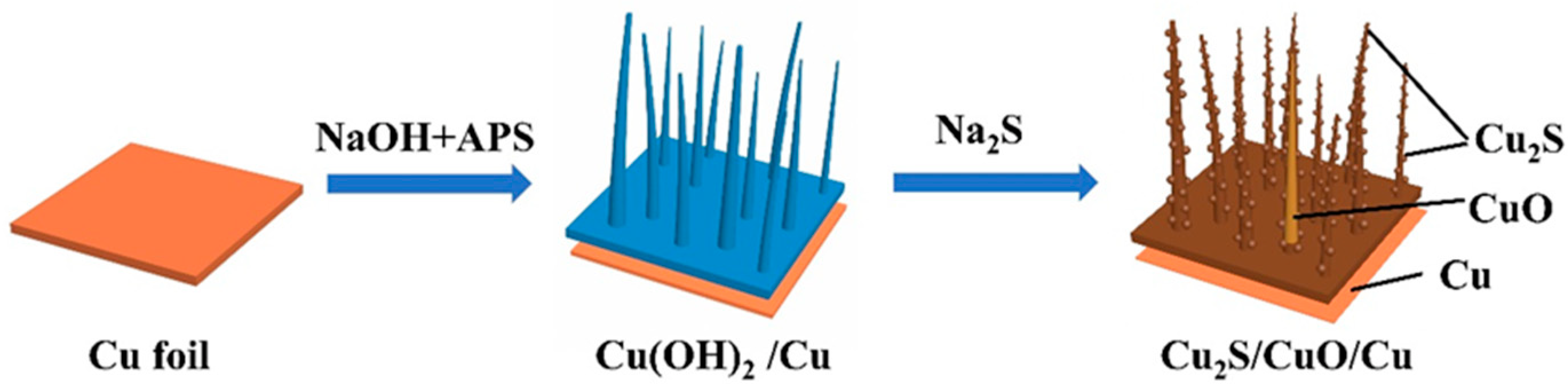
2.2. Preparation of Cu2S/CuO@Cu

Cu2S/CuO@Cu was fabricated by the impregnation method. Initially, Cu foil (1 × 1 cm2) was ultrasonically washed in a 2 M HNO3 aqueous solution for 1 min and cleaned in ethanol and deionized water before use. The cleaned Cu foil was immersed in 2 M aqueous solution of NaOH and 0.125 M APS for 15 min, and then cleaned by ethanol and deionized water sequentially. It was dried in air at 60 °C to obtain Cu(OH)2@Cu, which was named as CC-0. Next, Cu(OH)2@Cu was immersed in an aqueous solution of Na2S·9H2O for 30 min, washed with ethanol and deionized water several times, and dried in air at 60 °C. As per the used concentration of Na2S·9H2O, i.e., 1 M, 0.5 M, 0.25 M, 0.1 M, the sample was named as CCC-1, 2, 3, 4.

2.3. Sample Characterization

The surface of Cu2S/CuO@Cu was investigated using a transmission electron microscope (TEM—Talos F200X, Thermo Scientific, Waltham, MA, USA) and scanning electron microscope (SEM—JEOL JSM-7000F, Akishima, Japan). X-ray diffraction (XRD) measurement was performed to explore the crystalline structure of the samples using a diffractometer (D8 ADVANCE, Bruker, Mannheim, Germany) with Cu Kα radiation (1.54178 Å). X-ray photoelectron spectroscopy (XPS) measurements were carried out to investigate the chemical composition of Cu2S/CuO@Cu using a Thermo Fisher ESCALAB Xi+ instrument equipped with a monochromatic Al Kα X-ray source operating at 400 W. The adventitious C 1s peak (284.8 eV) was used as the binding energy reference. Raman spectra of the synthesized samples were recorded by HR800 spectrometer with a 532 nm laser source. Visible-infrared (vis-NIR) spectroscopic investigation of the sample was conducted using a UV-vis spectrophotometer (U-4100, Hitachi, Japan).

2.4. Photothermal Test

A 4.24 W Xenon lamp (LR-ISP808/4000mW-BH81497) was used as the light source, and the power density irradiated on the sample was calibrated as 0.025–3 W/cm2. The temperature of the sample was measured by Fluke Thermography (Ti10-14070064). The experimental setup for the photothermal test is shown in Figure S1.

2.5. FDTD Simulation

FDTD solution was utilized to set up the structure, and to simulate the optical absorption and distribution of the electric field. A total-field/scattered field (TFSF) source (400–1200 nm) was used as an incident field into the simulation region. Perfectly matched layer (PML) boundary was utilized to calculate the absorption cross-section. In our calculations, we have kept the mesh resolution as 10 nm.

3. Results and Discussion

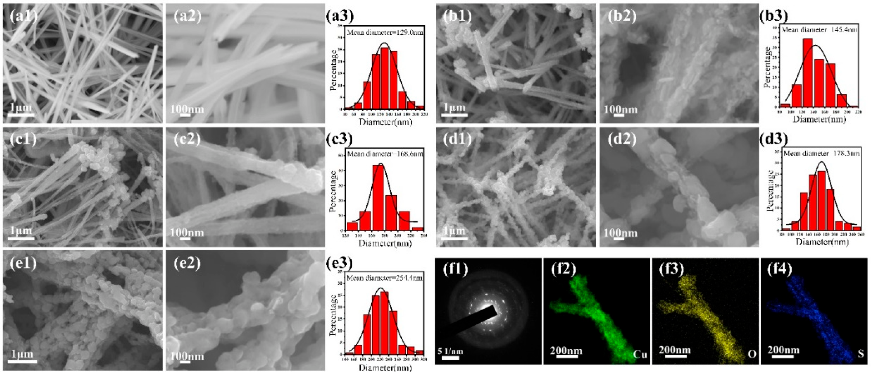
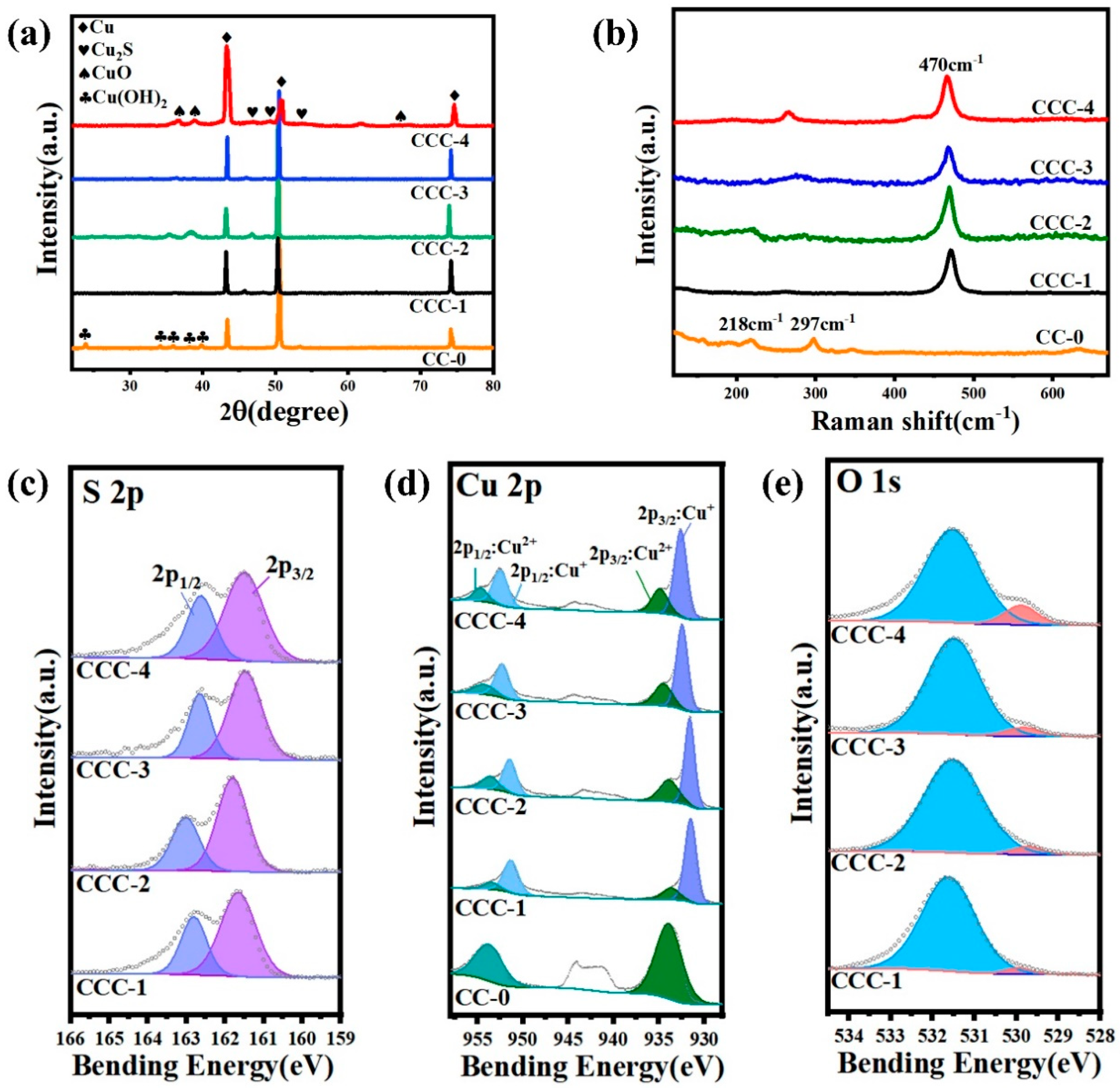
3.1. Characterization of Cu2S/CuO@Cu

The two-step impregnation procedure of Cu2S/CuO@Cu is schematically displayed in Figure 1. Under the effect of a strong alkaline solution, the crystallization of Cu(OH)2 nanowires occurs on the anodized Cu foil. The Cu(OH)2 nanowires were oxidized and formed CuO nanowire structures on the surface. The surface was further vulcanized to form Cu2S nanoparticles. The surface morphologies of Cu2S/CuO@Cu and Cu(OH)2@Cu are shown in Figure 2. From SEM images of Cu(OH)2 nanowires (Figure 2a1–a3), the wire shape of Cu(OH)2 is confirmed, and the nanowires exhibit size distributions of about 50–210 nm. Through vulcanization by Na2S, the Cu(OH)2 nanowires were converted to CuO nanowires covered with Cu2S nanoparticles. The components of Cu2S/CuO@Cu were further confirmed through elemental mapping (Figure 2f2–f4). With the growing concentration of Na2S, the diameter of the Cu2S nanowires is increased accordingly, as well as the size and number of Cu2S nanoparticles. The average Cu2S nanospheres diameters of CCC-1, 2, 3, 4 were measured to be 145.4 nm, 158.6 nm, 177.3 nm, and 254.5 nm, respectively.
The crystalline phases of Cu2S/CuO@Cu and Cu(OH)2@Cu were identified by XRD. As shown in Figure 3, the diffraction peaks of Cu(OH)2@Cu confirm the existence of Cu(OH)2 nanowires and Cu substrates; the diffraction peaks of Cu2S/CuO@Cu are ascribed to the following phases: Cu2S—nanoparticles, Cu2O—nanowires and Cu—substrates, indicating that the Cu(OH)2 nanowires were oxidized to Cu2O nanowires and then vulcanized to Cu2S nanoparticles on the surface.
The chemical composition of Cu2S/CuO@Cu was analyzed using the outcomes of XPS performed on CC-0 and CCC-x (x:1–4). Survey of the XPS spectrum clearly demonstrates that Cu2S/CuO@Cu is mainly composed of Cu, S, and O elements. Additionally, Cu(OH)2@Cu was also studied by XPS for comparative analysis, confirming the presence of Cu and O elements. To analyze the chemical valence of Cu2S/CuO@Cu, high-resolution Cu 2p spectra were investigated. The Cu 2p spectrum of CC-0 exhibits two binding energies at 934.0 eV and 954.4 eV, which are associated with Cu 2p3/2 and Cu 2p1/2 of Cu2+. For the CCC-x sample, the Cu 2p spectrum exhibits four peaks, in which two peaks at 932.6 eV—Cu 2p3/2 and 952.6 eV—Cu 2p1/2 of Cu+, and two others peaking at 934.7 eV and 954.7 eV, are ascribed to Cu 2p3/2 and Cu 2p1/2 of Cu2+. The XPS spectrum of S 2p is deconvoluted into two peaks, resulting in S 2p3/2 at 161.5 eV and S 2p1/2 at 162.6 eV, respectively. In addition, the O 1s spectrum presents two deconvoluted peaks at around 529.8 eV and 531.6 eV, which correspond to the absorbed oxygen from the environment and O2- binding with Cu2+ in CCC-x. Raman spectroscopy is an effective tool for studying molecular structure within nanostructures. Figure 3b shows the Raman spectrum of CCC-x; a strong and sharp band at 470 cm−1 is attributed to the vibrational mode of S-S bond stretching, confirming the Cu2S phase.
In order to evaluate the optical characteristics of Cu2S/CuO@Cu, the vis-NIR absorption spectrum was collected, as shown in Figure 4. The absorption spectrum shows low absorption in the visible region and strong absorbance in the NIR region, which means that the Cu2S/CuO@Cu has a strong response to NIR irradiation. It could be clearly visualized that the absorption spectrum was red-shifted as the concentration of Na2S was reduced from 1.0 M to 0.1 M.

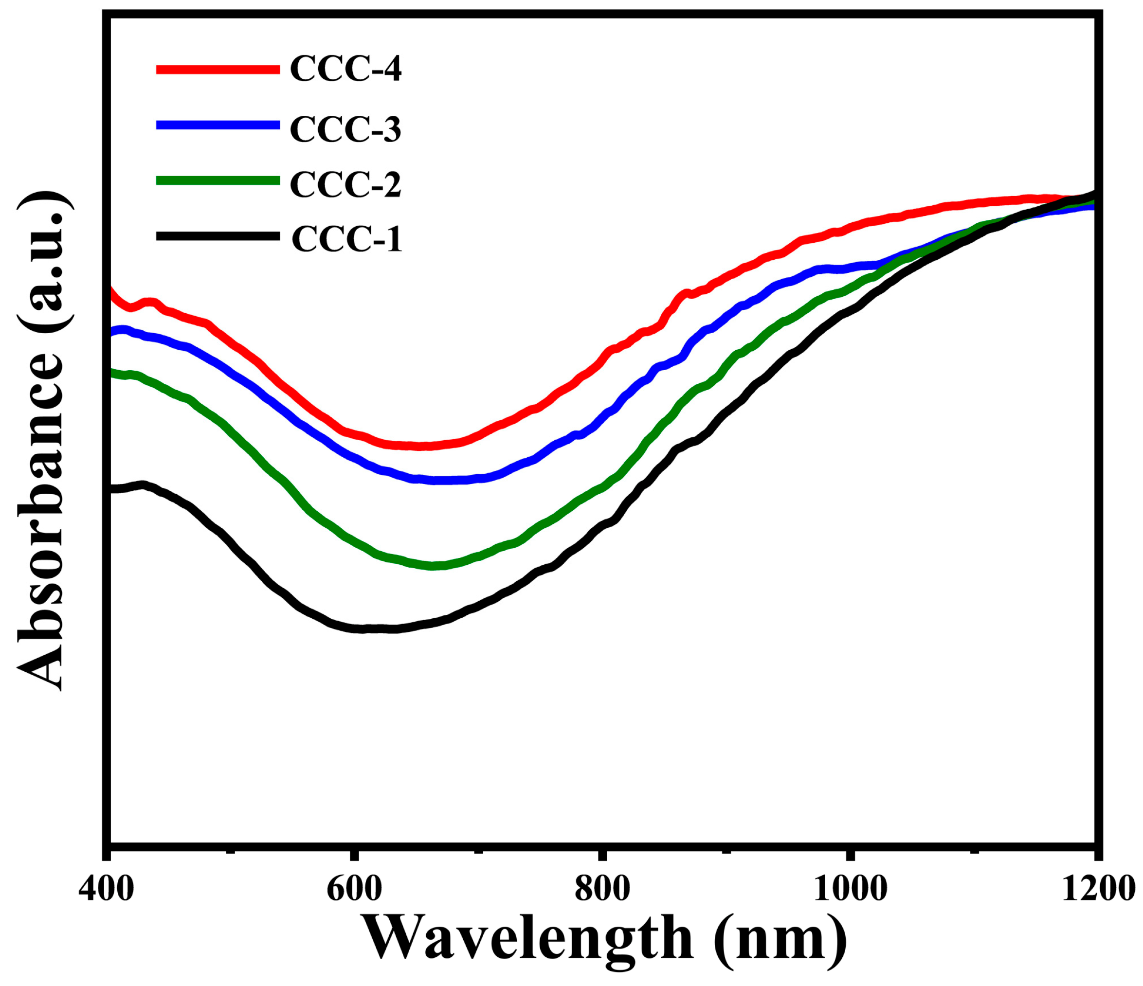
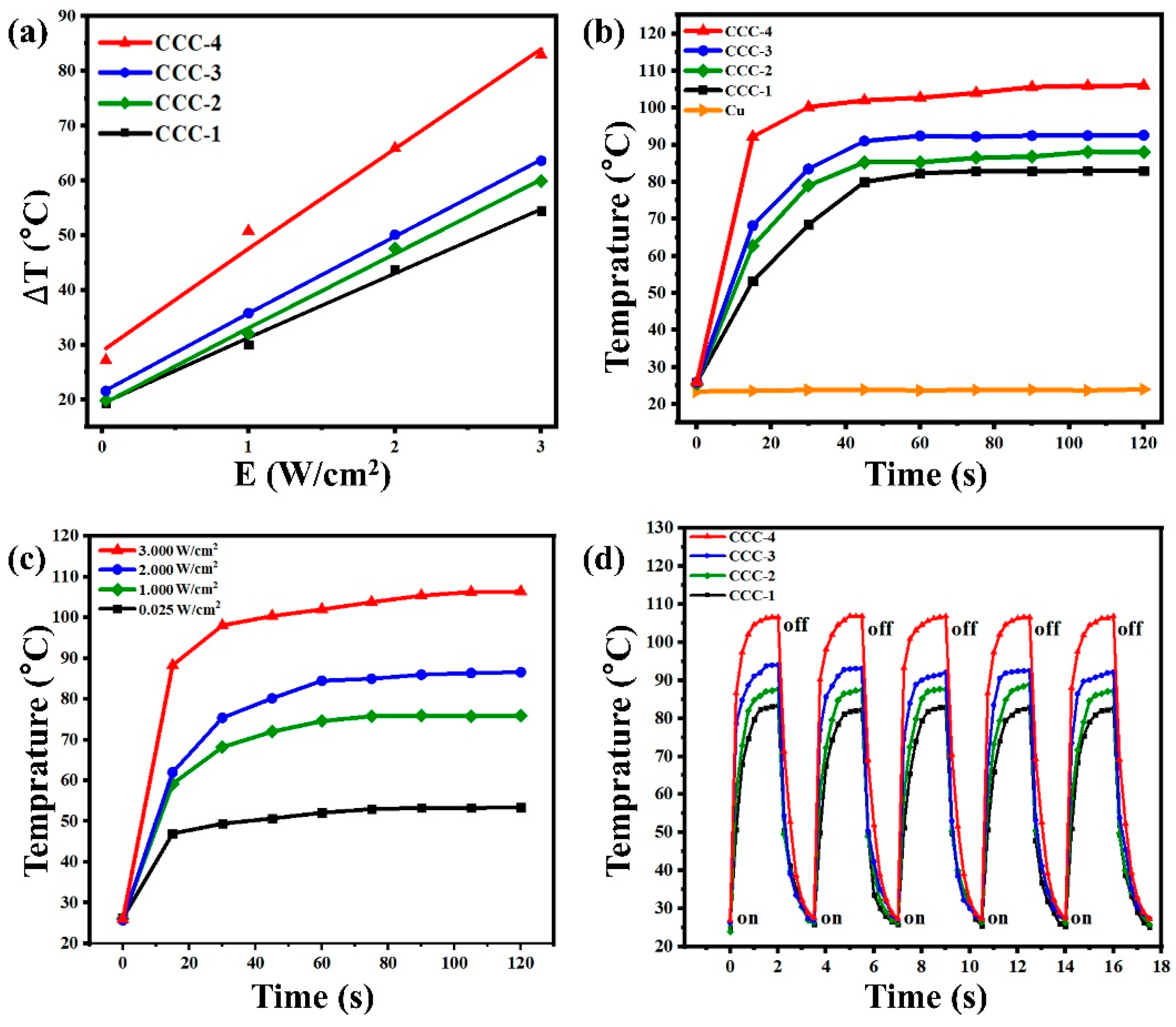
3.2. Photothermal Performance of Cu2S/CuO@Cu

At 808 nm laser irradiation, the laser-induced photothermal effect on Cu2S/CuO@Cu was studied at room temperature. The experiment was conducted using four different power densities (0.025 Wcm−2, 1.0 Wcm−2, 2.0 Wcm−2, 3.0 Wcm−2) of laser irradiation, as shown in Figure 5. As the power density rises, the temperature increases gradually. At 0.025 Wcm−2, samples CCC-x heated up from room temperature to 44.6 °C, 44.9 °C, 46.7 °C, and 54.4 °C within 120 s, respectively. Further, at 3.0 Wcm−2, the samples heated up to 83.0 °C, 88.1 °C, 92.6 °C, and 106.0 °C within 120 s. In all cases, a steep temperature rise was observed within the first 20 s of irradiation, indicating the fast optical response capability of Cu2S/CuO@Cu. The temperature of sample CCC-4 reached 84.0 °C, which is much higher than previously reported [28]. Notably, pure Cu foil at the power density of 3.0 Wcm−2 shows only 0.6 °C temperature gradient in 120 s. The photothermal stability of Cu2S/CuO@Cu was demonstrated through five cycles of laser irradiation. As shown in Figure 5d, the photothermal capability remains the same after five cycles of heating and cooling (heating 120 s and cooling 90 s for one cycle); this result confirms the excellent photothermal stability of Cu2S/CuO@Cu.

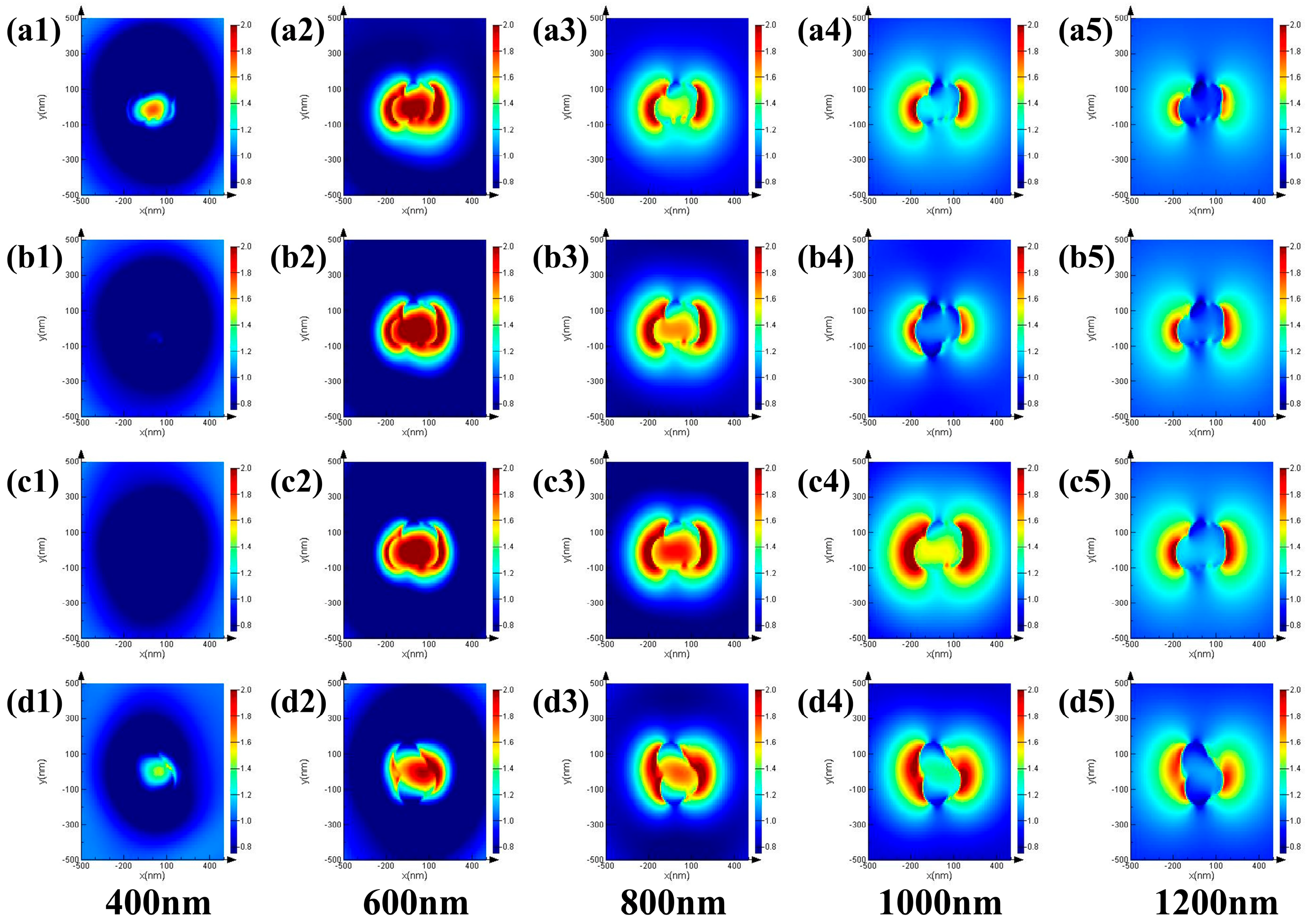
3.3. Numerical Simulation of Cu2S/CuO@Cu

FDTD simulation of optical absorption and electric field distributions was studied to investigate the photothermal role of Cu2S/CuO@Cu. Figure S2 shows the comparison of the absorbance results obtained from FDTD simulation with the experimental measurements. The results are consistent, indicating the accuracy of the proposed model for purposes of investigating the electric field distribution of Cu2S/CuO@Cu. The structural model of Cu2S/CuO@Cu was constructed (Figure S3), and the electric field distributions (E/E0) of Cu2S/CuO@Cu were simulated at an incident light with a wavelength of 400–1200 nm. E and E0 were specified as reinforced electric field and incident electric field, respectively. Figure 6 shows the cross-sectional view of the electric field distributions of Cu2S/CuO@Cu.
As the simulated irradiation wavelength was increased from 400 nm to 1200 nm, the electric field distribution of Cu2S/CuO@Cu increased at first and then decreased. At 800 nm of irradiation, both the area and intensity of the electric field distribution were high; 808 nm laser light stimulated the strongest photothermal effect of Cu2S/CuO@Cu. Moreover, from the electric field distributions of CCC-x (x:1, 2, 3, 4), as the size of Cu2S nanosphere and nanowire size increased, the electric field distribution increased, leading to higher photothermal performance. Among all the Cu2S/CuO@Cu samples, CCC-4 demonstrated the highest electric field distribution numerically, which is consistent with the conducted experiment.

4. Conclusions

In summary, we have developed a simple two-step impregnation method to synthesize Cu2S nanoparticles grown on Cu-based substrate with controlled size by adjusting the concentration of Na2S. The as-synthesized Cu2S/CuO@Cu exhibited high performance in terms of photothermal conversion ability, with the maximum temperature raised to 106.0 °C from room temperature. The photothermal stability of Cu2S/CuO@Cu was proved through five heating-cooling cycles. Moreover, FDTD simulation of optical absorption and electric field distributions proved that the developed experimental condition enables the best photothermal performance of Cu2S/CuO@Cu.

Supplementary Materials

The following supporting information can be downloaded at: https://www.mdpi.com/article/10.3390/nano13071260/s1, Figure S1: Experimental setup for the photothermal experiment: (a) side view and (b) vertical view.; Figure S2: FDTD simulation (circle) and experimental data (solid line) of optical absorbance of CCC-x.; Figure S3: Structural model of the Cu2S/CuO@Cu in the FDTD simulation.

Author Contributions

Conceptualization, C.K.; investigation, H.M. and Y.W.; resources, Z.Y. and C.Z.; data curation, H.M. and Y.W.; writing—original draft preparation, H.M. and Y.W.; writing—review and editing, C.K.; supervision, C.K.; project administration, C.K.; funding acquisition, C.K. All authors have read and agreed to the published version of the manuscript.

Funding

This research was funded by [Shccig-Qinling Program] grant number [2021JLM-27], [Lanzhou University-Jinchuan Group Chemical Co., Ltd. Chemical Environmental Protection Industry Joint Laboratory] grant number [(20)0837].

Data Availability Statement

The data are not publicly available due to the relevant project regulations.

Conflicts of Interest

The authors declare no conflict of interest.

References

  1. Mathuri, S.; Zhu, Y.; Margoni, M.M.; Li, X. Semiconducting Nanoparticles: Single Entity Electrochemistry and Photoelectrochemistry. Front. Chem. 2021, 9, 688320. [Google Scholar] [CrossRef]
  2. Joe, J.; Yang, H.; Bae, C.; Shin, H. Metal Chalcogenides on Silicon Photocathodes for Efficient Water Splitting: A Mini Overview. Catalysts 2019, 9, 149. [Google Scholar] [CrossRef] [Green Version]
  3. Tan, C.; Lai, Z.; Zhang, H. Ultrathin Two-Dimensional Multinary Layered Metal Chalcogenide Nanomaterials. Adv. Mater. 2017, 29, 1701392. [Google Scholar] [CrossRef]
  4. Chen, Y.; Kivisaari, P.; Pistol, M.E.; Anttu, N. Optimization of the short-circuit current in an InP nanowire array solar cell through opto-electronic modeling. Nanotechnology 2016, 27, 435404. [Google Scholar] [CrossRef] [Green Version]
  5. Du, C.; Huang, H.; Jian, J.; Wu, Y.; Shang, M.; Song, W. Enhanced electrocatalytic hydrogen evolution performance of MoS2 ultrathin nanosheets via Sn doping. Appl. Catal. A Gen. 2017, 538, 1–8. [Google Scholar] [CrossRef]
  6. Cheng, L.; Liu, J.; Gu, X.; Gong, H.; Shi, X.; Liu, T.; Wang, C.; Wang, X.; Liu, G.; Xing, H.; et al. PEGylated WS2 nanosheets as a multifunctional theranostic agent for in vivo dual-modal CT/photoacoustic imaging guided photothermal therapy. Adv. Mater. 2014, 26, 1886–1893. [Google Scholar] [CrossRef]
  7. Xiang, G.; Xia, Q.; Liu, X.; Wang, Y.; Jiang, S.; Li, L.; Zhou, X.; Ma, L.; Wang, X.; Zhang, J. Upconversion nanoparticles modified by Cu2S for photothermal therapy along with real-time optical thermometry. Nanoscale 2021, 13, 7161–7168. [Google Scholar] [CrossRef]
  8. Adjogri, S.J.; Meyer, E.L. Chalcogenide Perovskites and Perovskite-Based Chalcohalide as Photoabsorbers: A Study of Their Properties, and Potential Photovoltaic Applications. Materials 2021, 14, 7857. [Google Scholar] [CrossRef]
  9. Liu, S.; Wang, L.; Zhao, B.; Wang, Z.; Wang, Y.; Sun, B.; Liu, Y. Doxorubicin-loaded Cu2S/Tween-20 nanocomposites for light-triggered tumor photothermal therapy and chemotherapy. RSC Adv. 2020, 10, 26059–26066. [Google Scholar] [CrossRef]
  10. Alami, A.H.; Aokal, K. Enhancement of spectral absorption of solar thermal collectors by bulk graphene addition via high-pressure graphite blasting. Energy Convers. Manag. 2018, 156, 757–764. [Google Scholar] [CrossRef]
  11. Shan, X.; Zhao, A.; Lin, Y.; Hu, Y.; Di, Y.; Liu, C.; Gan, Z. Low-Cost, Scalable, and Reusable Photothermal Layers for Highly Efficient Solar Steam Generation and Versatile Energy Conversion. Adv. Sustain. Syst. 2020, 4, 1900153. [Google Scholar] [CrossRef]
  12. Chen, H.; Shi, R.; Zhang, T. Nanostructured Photothermal Materials for Environmental and Catalytic Applications. Molecules 2021, 26, 7552. [Google Scholar] [CrossRef] [PubMed]
  13. Wang, P. Emerging investigator series: The rise of nano-enabled photothermal materials for water evaporation and clean water production by sunlight. Environ. Sci. Nano 2018, 5, 1078–1089. [Google Scholar] [CrossRef] [Green Version]
  14. Phan, L.M.T.; Vo, T.A.T.; Hoang, T.X.; Cho, S. Graphene Integrated Hydrogels Based Biomaterials in Photothermal Biomedicine. Nanomaterials 2021, 11, 906. [Google Scholar] [CrossRef] [PubMed]
  15. Ou, H.; Li, J.; Chen, C.; Gao, H.; Xue, X.; Ding, D. Organic/polymer photothermal nanoagents for photoacoustic imaging and photothermal therapy in vivo. Sci. China Mater. 2019, 62, 1740–1758. [Google Scholar] [CrossRef] [Green Version]
  16. De Solorzano, I.O.; Prieto, M.; Mendoza, G.; Alejo, T.; Irusta, S.; Sebastian, V.; Arruebo, M. Microfluidic Synthesis and Biological Evaluation of Photothermal Biodegradable Copper Sulfide Nanoparticles. ACS Appl. Mater. Interfaces 2016, 8, 21545–21554. [Google Scholar] [CrossRef] [PubMed] [Green Version]
  17. Gu, Y.; Li, X.; Li, X.; Yao, Z.; Lu, S.; Wu, X. Facile Preparation of Cu2S/Cu Mesh For High-performance Solar Water Evaporation. ChemistrySelect 2021, 6, 7901–7905. [Google Scholar] [CrossRef]
  18. Neelgund, G.M.; Oki, A.; Bandara, S.; Carson, L. Photothermal effect and cytotoxicity of CuS nanoflowers deposited over folic acid conjugated nanographene oxide. J. Mater. Chem. B 2021, 9, 1792–1803. [Google Scholar] [CrossRef]
  19. Yoon, D.; Yoo, S.; Nam, K.S.; Baik, H.; Lee, K.; Park, Q.H. Plasmon Enhanced Direct Bandgap Emissions in Cu7S4 @Au2S@Au Nanorings. Small 2016, 12, 5728–5733. [Google Scholar] [CrossRef]
  20. Poulose, A.C.; Veeranarayanan, S.; Mohamed, M.S.; Nagaoka, Y.; Aburto, R.R.; Mitcham, T.; Ajayan, P.M.; Bouchard, R.R.; Sakamoto, Y.; Yoshida, Y.; et al. Multi-stimuli responsive Cu2S nanocrystals as trimodal imaging and synergistic chemo-photothermal therapy agents. Nanoscale 2015, 7, 8378–8388. [Google Scholar] [CrossRef] [PubMed] [Green Version]
  21. Tian, J.; Qiao, R.; Xiong, K.; Zhang, W.; Chen, L. A bioinspired Au-Cu1.97S/Cu2S film with efficient low-angle-dependent and thermal-assisted photodetection properties. iScience 2021, 24, 102167. [Google Scholar] [CrossRef] [PubMed]
  22. Leal-Perez, J.E.; Flores-Valenzuela, J.; Vargas-Ortíz, R.A.; Alvarado-Beltrán, C.G.; Hurtado-Macias, A.; Almaral-Sánchez, J.L. Synthesis of Cu2S Ultrasmall Nanoparticles in Zeolite 4A Nanoreactor. J. Clust. Sci. 2022, 159, 1–6. [Google Scholar] [CrossRef]
  23. Rao, V.N.; Ravi, P.; Sathish, M.; Sakar, M.; Yang, B.L.; Yang, J.-M.; Kumari, M.M.; Shankar, M.V. Titanate quantum dots-sensitized Cu2S nanocomposites for superficial H2 production via photocatalytic water splitting. Int. J. Hydrog. Energy 2022, 47, 40379–40390. [Google Scholar] [CrossRef]
  24. Wang, L.; Ji, L.; Li, W.; Zhang, K.; Xu, H.; Huang, W.; Yan, N.; Qu, Z. Fabrication of Cu2S hollow nanocages with enhanced high-temperature adsorption activity and recyclability for elemental mercury capture. Chem. Eng. J. 2022, 47, 130935. [Google Scholar] [CrossRef]
  25. Ahmed, H.S.; Mohammed, R.Y. The Effect of Deposition Parameters on Morphological and Optical Properties of Cu2S Thin Films Grown by Chemical Bath Deposition Technique. Photonics 2022, 9, 161. [Google Scholar] [CrossRef]
  26. Zhang, Y.; Hu, L.; Zhang, Y.; Wang, X.; Wang, H. Snowflake-Like Cu2S/MoS2/Pt heterostructure with near infrared photothermal-enhanced electrocatalytic and photoelectrocatalytic hydrogen production. Appl. Catal. B Environ. 2022, 315, 121540. [Google Scholar] [CrossRef]
  27. Wang, X.; Lv, F.; Li, T.; Han, Y.; Yi, Z.; Liu, M.; Chang, J.; Wu, C. Electrospun Micropatterned Nanocomposites Incorporated with Cu2S Nanoflowers for Skin Tumor Therapy and Wound Healing. ACS Nano 2017, 11, 11337–11349. [Google Scholar] [CrossRef]
  28. Zhang, Z.; Suo, H.; Zhao, X.; Sun, D.; Fan, L.; Guo, C. NIR-to-NIR Deep Penetrating Nanoplatforms Y2O3:Nd(3+)/Yb(3+)@SiO2@Cu2S toward Highly Efficient Photothermal Ablation. ACS Appl. Mater. Interfaces 2018, 10, 14570–14576. [Google Scholar] [CrossRef]
Figure 1. Schematic illustration of the fabrication process of Cu2S/CuO@Cu.
Nanomaterials 13 01260 g001
Figure 2. SEM images and size distributions of (a1a3) CC-0, (b1b3) CCC-1, (c1c3) CCC-2, (d1d3) CCC-3, (e1e3) CCC-5; (f1) SAED and (f2f4) elemental mapping of CCC-3.
Nanomaterials 13 01260 g002
Figure 3. (a) XRD pattern, (b) Raman spectra, (ce) XPS spectra of CCC-x and CC-0.
Nanomaterials 13 01260 g003
Figure 4. The optical absorbance of CCC-x.
Nanomaterials 13 01260 g004
Figure 5. (a) Temperature gradient in CCC-x at 0.025, 1.0, 2.0, 3.0 W/cm2 laser irradiation, (b) temperature gradient in CCC-x and Cu at 3.0 W/cm2 laser irradiation for 120 s, (c) temperature gradient in CCC-4 at 0.025, 1.0, 2.0, 3.0 W/cm2 laser irradiation for 120 s, and (d) photothermal cycling test of CCC-x at 3.0 W/cm2 laser irradiation.
Nanomaterials 13 01260 g005
Figure 6. FDTD simulation of electric field distribution of (a1a5) CCC-1, (b1b5) CCC-2, (c1c5) CCC-3, and (d1d5) CCC-4 at different radiation wavelengths (400 nm, 600 nm, 800 nm, 1000 nm, and 1200 nm).
Nanomaterials 13 01260 g006
Disclaimer/Publisher’s Note: The statements, opinions and data contained in all publications are solely those of the individual author(s) and contributor(s) and not of MDPI and/or the editor(s). MDPI and/or the editor(s) disclaim responsibility for any injury to people or property resulting from any ideas, methods, instructions or products referred to in the content.

