
Transverse Magnetic Surface Plasmons in Graphene Nanoribbon Qubits: The Influence of a VO2 Substrate
Abstract
:1. Introduction
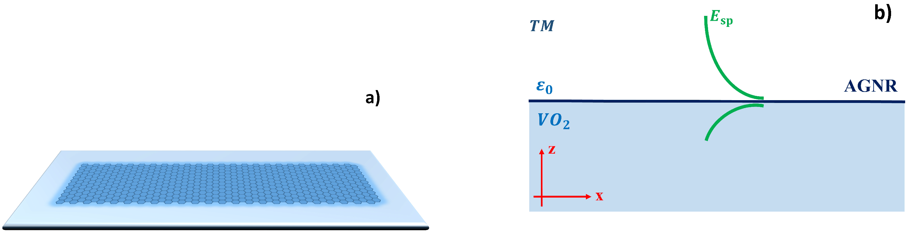
2. Formalism
3. Results and Discussion
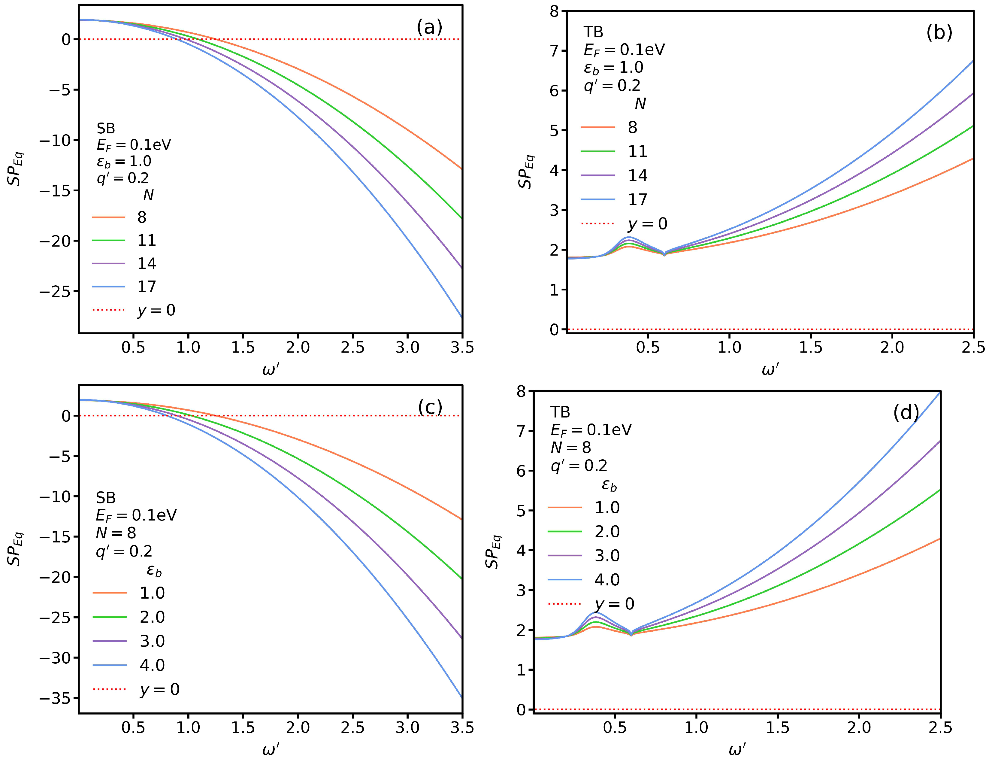
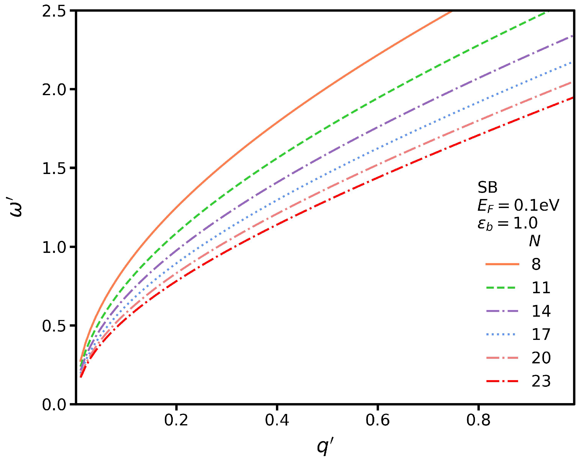
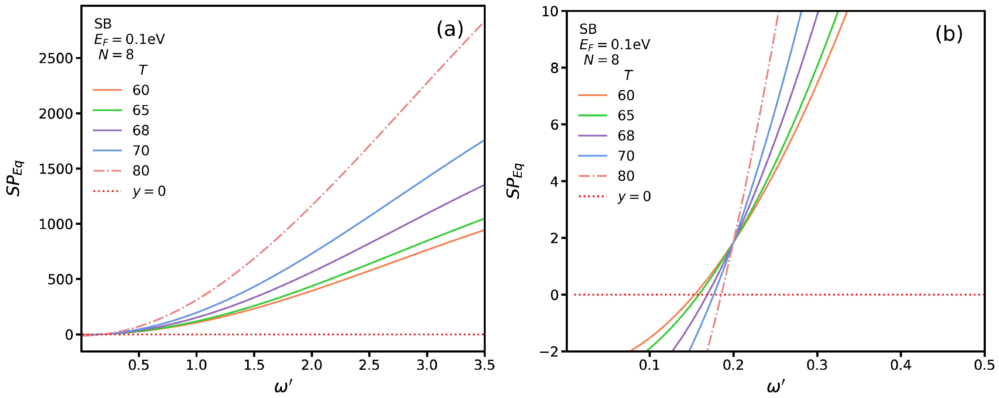
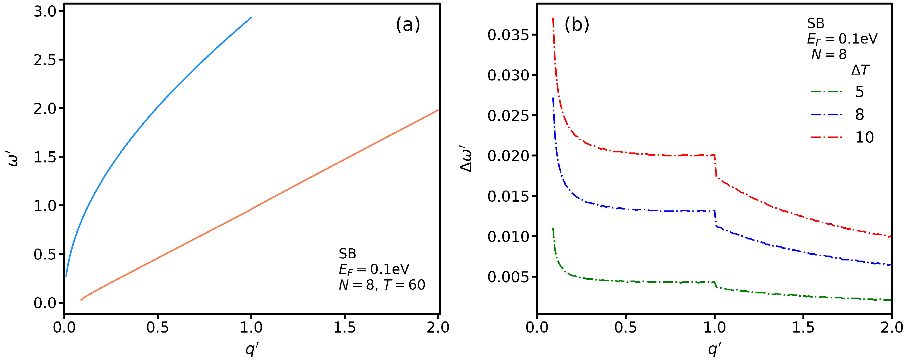
3.1. Substrates with Constant Permittivity
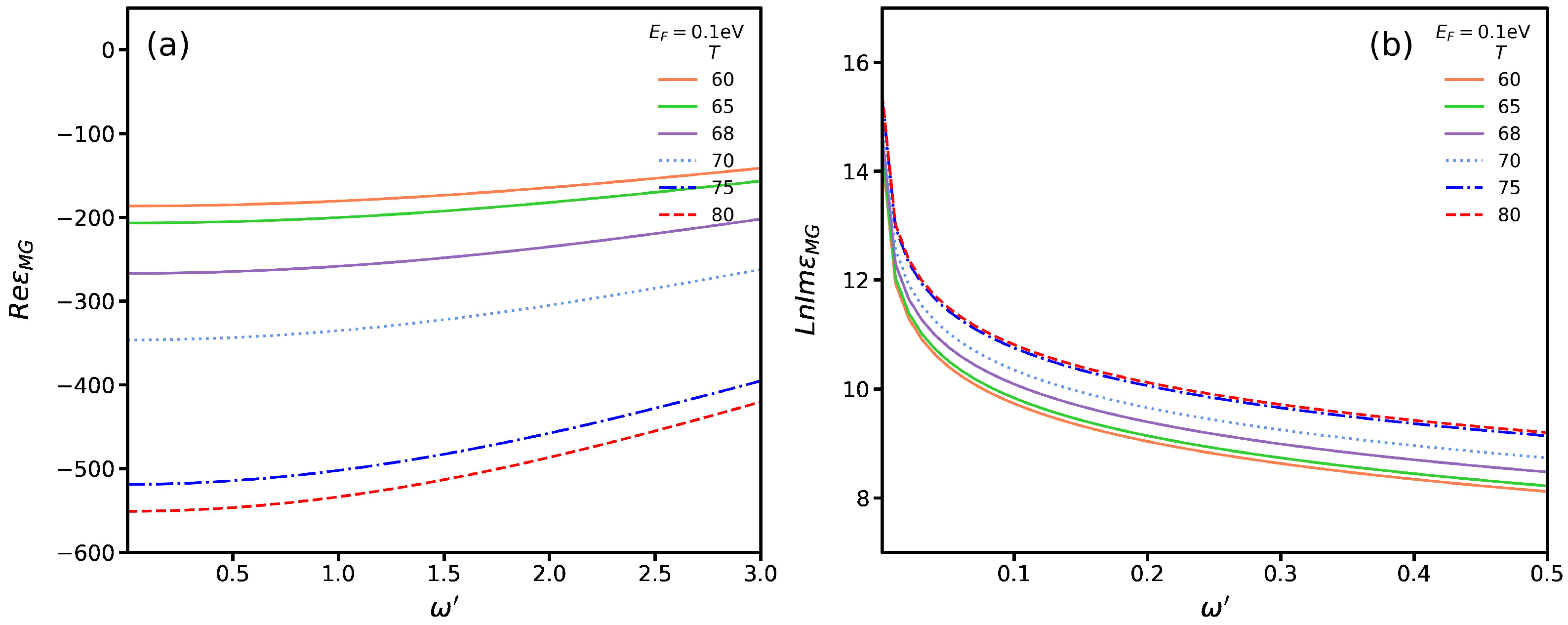
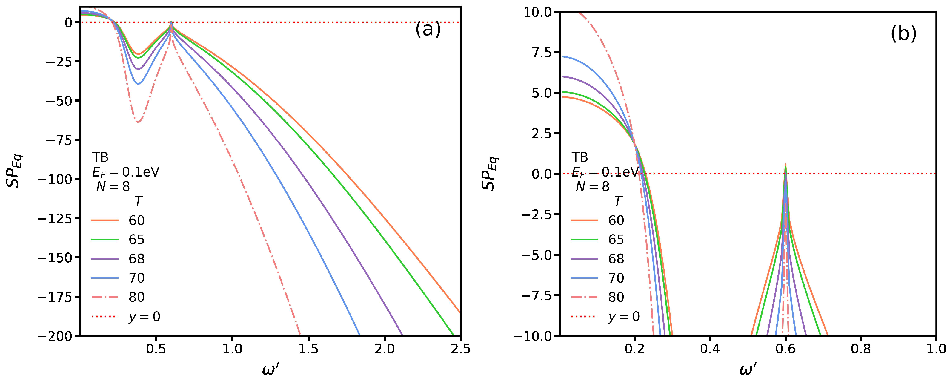
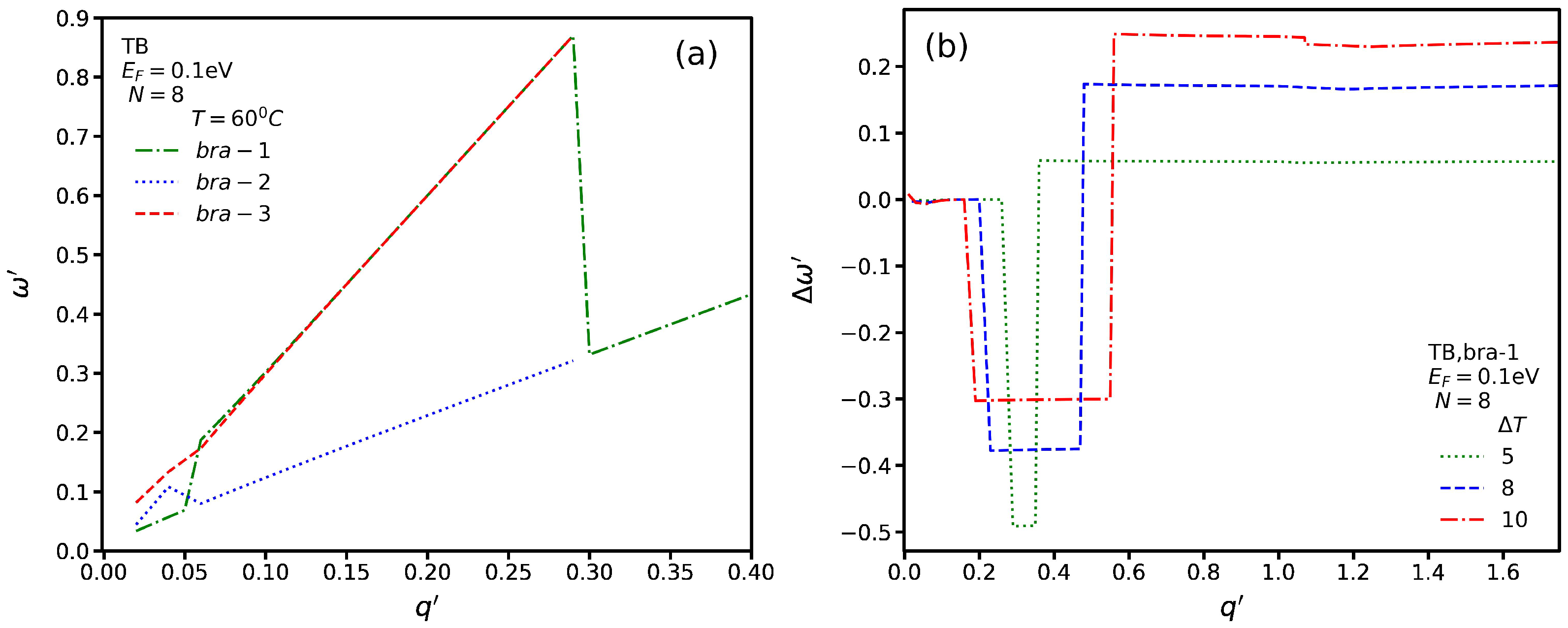
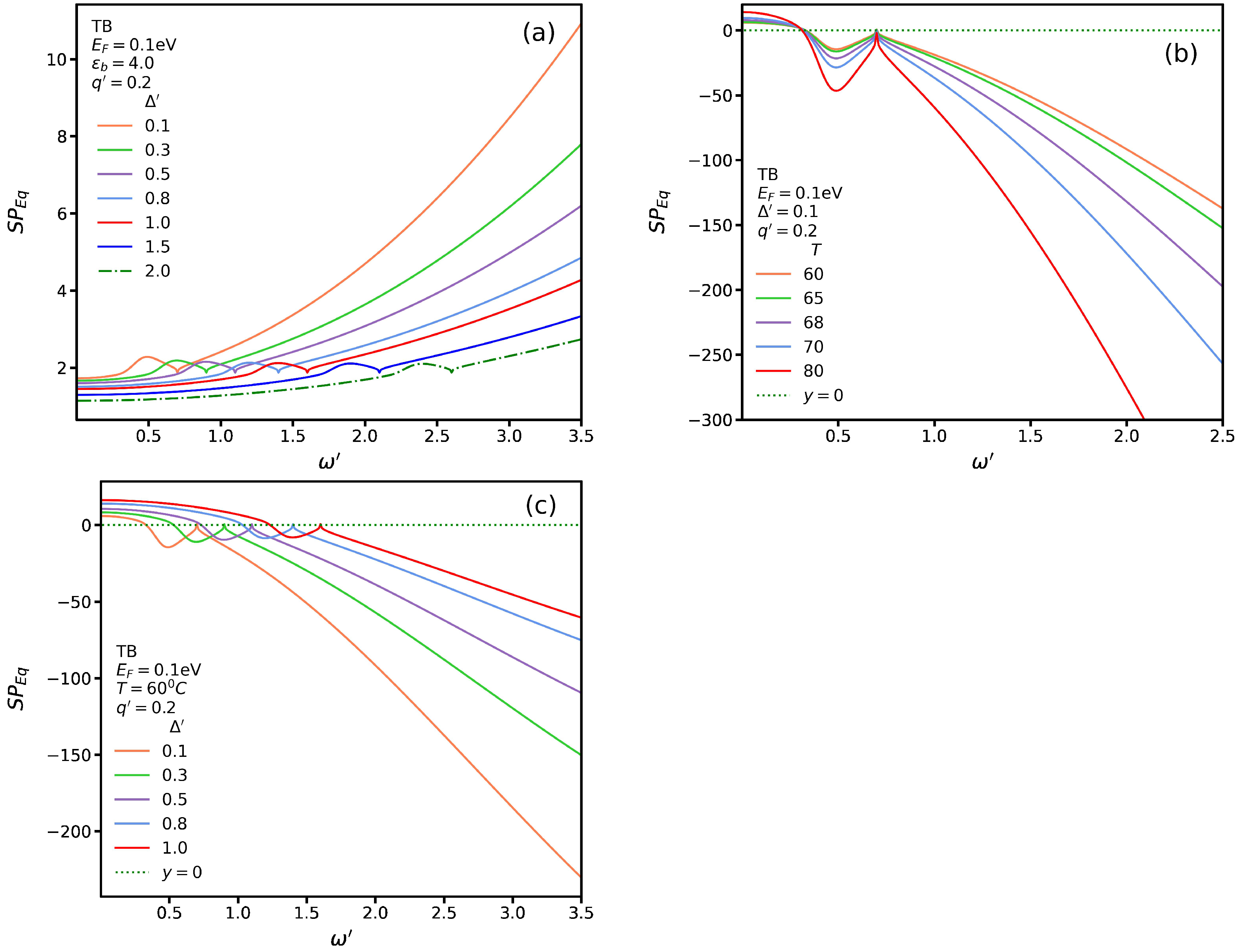
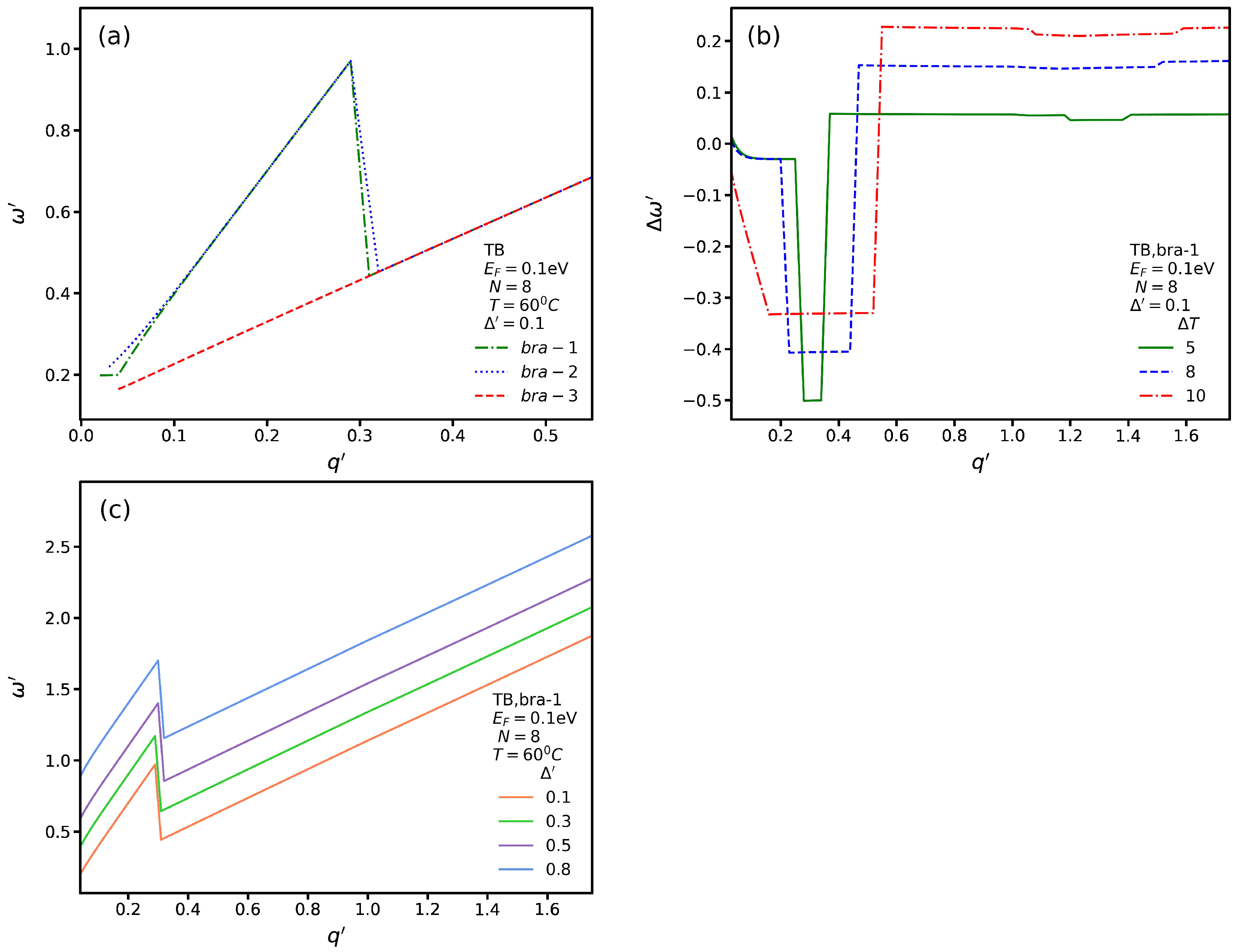
3.2. Substrates with Phase-Change Functionality: VO2
4. Summary
Author Contributions
Funding
Data Availability Statement
Conflicts of Interest
References
- Hilbert, M.; López, P. The World’s Technological Capacity to Store, Communicate, and Compute Information. Science 2011, 332, 60–65. [Google Scholar] [CrossRef] [PubMed]
- Francis, X.; Diebold, A. Personal Perspective on the Origin(s) and Development of ’Big Data’: The Phenomenon, the Term, and the Discipline, Second Version. Ssrn Electron. J. 2012. [Google Scholar] [CrossRef]
- Sabina, L. Scientific Research and Big Data. In The Stanford Encyclopedia of Philosophy; Summer Edition 2020; Stanford University: Stanford, CA, USA, 2020; Available online: https://plato.stanford.edu/archives/sum2020/entries/science-big-data/ (accessed on 1 October 2022).
- Fathi, M.; Kashani, M.H.; Jameii, S.M.; Mahdipour, E. Big Data Analytics in Weather Forecasting: A Systematic Review. Arch. Comput. Methods Eng. 2021, 29, 1247–1275. [Google Scholar] [CrossRef]
- Yan, Z.; Ismail, H.; Chen, L.; Zhao, X.; Wang, L. The application of big data analytics in optimizing logistics: A developmental perspective review. J. Data Inf. Manag. 2019, 1, 33–43. [Google Scholar] [CrossRef]
- Cockcroft, S.; Russell, M. Big Data Opportunities for Accounting and Finance Practice and Research. Aust. Account. Rev. 2018, 28, 323–333. [Google Scholar] [CrossRef]
- Tan, J.; Osborne, B. Analisys of big data from space. Int. Arch. Photogramm. Remote. Sens. Spat. Inf. Sci. 2017, XLII-2/W7, 1367–1371. [Google Scholar] [CrossRef]
- Tormay, P. Big Data in Pharmaceutical R&D: Creating a Sustainable R&D Engine. Pharm. Med. 2015, 29, 87–92. [Google Scholar] [CrossRef]
- O’Leary, D.E. Artificial Intelligence and Big Data. IEEE Intell. Syst. 2013, 28, 96–99. [Google Scholar] [CrossRef]
- Danda, B. Rawat and Ronald Doku and Moses Garuba, Cybersecurity in Big Data Era: From Securing Big Data to Data-Driven Security. IEEE Trans. Serv. Comput. 2011, 14, 2055–2072. [Google Scholar] [CrossRef]
- Meindl, J.D.; Chen, Q.; Davis, J.A. Limits on Silicon Nanoelectronics for Terascale Integration. Science 2001, 293, 2044–2049. [Google Scholar] [CrossRef]
- Keyes, R.W. Fundamental limits of silicon technology. Proc. IEEE 2001, 89, 227–239. [Google Scholar] [CrossRef]
- Sodan, A.C.; Machina, J.; Deshmeh, A.; Macnaughton, K.; Esbaugh, B. Parallelism via Multithreaded and Multicore CPUs. Computer 2010, 43, 24–32. [Google Scholar] [CrossRef]
- Zhong, H.-S.; Wang, H.; Deng, Y.-H.; Chen, M.-C.; Peng, L.-C.; Luo, Y.-H.; Qin, J.; Wu, D.; Ding, X.; Hu, Y.; et al. Quantum computational advantage using photons. Science 2020, 370, 1460–1463. [Google Scholar] [CrossRef]
- Gibney, E. Hello quantum world! Google publishes landmark quantum supremacy claim. Nature 2019, 574, 461–462. [Google Scholar] [CrossRef]
- Kalfus, W.D.; Lee, D.F.; Ribeill, G.J.; Fallek, S.D.; Wagner, A.; Donovan, B.; Riste, D.; Ohki, T.A. High-Fidelity Control of Superconducting Qubits Using Direct Microwave Synthesis in Higher Nyquist Zones. IEEE Trans. Quantum Eng. 2020, 1, 1–12. [Google Scholar] [CrossRef]
- Kjaergaard, M.; Schwartz, M.E.; Braumüller, J.; Krantz, P.; Wang, J.I.-J.; Gustavsson, S.; Oliver, W.D. Superconducting Qubits: Current State of Play. Annu. Rev. Condens. Matter Phys. 2020, 11, 369–395. [Google Scholar] [CrossRef]
- Chen, Z.; Satzinger, K.J.; Atalaya, J.; Korotkov, A.N.; Dunsworth, A.; Sank, D.; Quintana, C.; McEwen, M.; Barends, R.; Klimov, P.V. Exponential suppression of bit or phase errors with cyclic error correction. Nature 2021, 595, 383–387. [Google Scholar] [CrossRef]
- Calafell, I.A.; Cox, J.D.; Radonjić, M.; Saavedra, J.R.M.; de Abajo, F.J.G.; Rozema, L.A.; Walther, P. Quantum computing with graphene plasmons. npj Quantum Inf. 2019, 5, 37. [Google Scholar] [CrossRef]
- Shangguan, Q.; Chen, Z.; Yang, H.; Cheng, S.; Yang, W.; Yi, Z.; Wu, X.; Wang, S.; Yi, Y.; Wu, P. Design of Ultra-Narrow Band Graphene Refractive Index Sensor. Sensors 2022, 22, 6483. [Google Scholar] [CrossRef]
- Cheng, Z.; Liao, J.; He, B.; Zhang, F.; Zhang, F.; Huang, X.; Zhou, L. One-Step Fabrication of Graphene Oxide Enhanced Magnetic Composite Gel for Highly Efficient Dye Adsorption and Catalysis. Acs Sustain. Chem. Eng. 2015, 3, 1677–1685. [Google Scholar] [CrossRef]
- Shangguan, Q.; Zhao, Y.; Song, Z.; Wang, J.; Yang, H.; Chen, J.; Liu, C.; Cheng, S.; Yang, W.; Yi, Z. High sensitivity active adjustable graphene absorber for refractive index sensing applications. Diam. Relat. Mater. 2022, 128, 109273. [Google Scholar] [CrossRef]
- Zhang, Z.; Cai, R.; Long, F.; Wang, J. Development and application of tetrabromobisphenol A imprinted electrochemical sensor based on graphene/carbon nanotubes three-dimensional nanocomposites modified carbon electrode. Talanta 2015, 134, 435–442. [Google Scholar] [CrossRef] [PubMed]
- Constant, T.J.; Hornett, S.M.; Chang, D.E.; Hendry, E. All-optical generation of surface plasmons in graphene. Nat. Phys. 2015, 12, 124–127. [Google Scholar] [CrossRef]
- Bao, Q.; Loh, K.P. Graphene Photonics, Plasmonics, and Broadband Optoelectronic Devices. ACS Nano 2012, 6, 3677–3694. [Google Scholar] [CrossRef]
- Ju, L.; Geng, B.; Horng, J.; Girit, C.; Martin, M.; Hao, Z.; Bechtel, H.A.; Liang, X.; Zettl, A.; Shen, Y.R.; et al. Graphene plasmonics for tunable terahertz metamaterials. Nat. Nanotechnol. 2011, 6, 630–634. [Google Scholar] [CrossRef]
- Koppens, F.H.L.; Chang, D.E.; de Abajo, F.J.G. Graphene Plasmonics: A Platform for Strong Light—Matter Interactions. Nano Lett. 2011, 11, 3370–3377. [Google Scholar] [CrossRef]
- DRodrigo, a.; Limaj, O.; Janner, D.; Etezadi, D.; de Abajo, F.J.G.; Pruneri, V.; Altug, H. Mid-infrared plasmonic biosensing with graphene. Science 2015, 349, 165–168. [Google Scholar] [CrossRef]
- Woessner, A.; Lundeberg, M.B.; Gao, Y.; Principi, A.; Alonso-González, P.; Carrega, M.; Watanabe, K.; Taniguchi, T.; Vignale, G.; Polini, M.; et al. Highly confined low-loss plasmons in graphene–boron nitride heterostructures. Nat. Mater. 2014, 14, 421–425. [Google Scholar] [CrossRef]
- Low, T.; Avouris, P. Low and Phaedon Avouris, Graphene Plasmonics for Terahertz to Mid-Infrared Applications. ACS Nano 2014, 8, 1086–1101. [Google Scholar] [CrossRef]
- Mittendorff, M.; Winnerl, S.; Murphy, T.E. 2D THz Optoelectronics. Adv. Opt. Mater. 2020, 9, 2001500. [Google Scholar] [CrossRef]
- Wang, S.; Yoo, S.; Zhao, S.; Zhao, W.; Kahn, S.; Cui, D.; Wu, F.; Jiang, L.; Utama, M.I.B.; Li, H.; et al. Gate-tunable plasmons in mixed-dimensional van der Waals heterostructures. Nat. Commun. 2021, 12, 5039. [Google Scholar] [CrossRef]
- Zhang, J.; Zhang, Z.; Song, X.; Zhang, H.; Yang, J. Infrared Plasmonic Sensing with Anisotropic Two-Dimensional Material Borophene. Nanomaterials 2021, 11, 1165. [Google Scholar] [CrossRef]
- Quackenbush, N.F.; Tashman, J.W.; Mundy, J.A.; Sallis, S.; Paik, H.; Misra, R.; Moyer, J.A.; Guo, J.-H.; Fischer, D.A.; Woicik, J.C.; et al. Nature of the Metal Insulator Transition in Ultrathin Epitaxial Vanadium Dioxide. Nano Lett. 2013, 13, 4857–4861. [Google Scholar] [CrossRef]
- Whittaker, L.; Patridge, C.J.; Banerjee, S. Microscopic and Nanoscale Perspective of the Metal-Insulator Phase Transitions of VO2: Some New Twists to an Old Tale. J. Phys. Chem. Lett. 2011, 2, 745–758. [Google Scholar] [CrossRef]
- Wei, J.; Wang, Z.; Chen, W.; Cobden, D.H. New aspects of the metal–insulator transition in single-domain vanadium dioxide nanobeams. Nat. Nanotechnol. 2009, 4, 420–424. [Google Scholar] [CrossRef]
- Eyert, V. VO2: A Novel View from Band Theory. Phys. Rev. Lett. 2011, 107, 016401. [Google Scholar] [CrossRef]
- Haverkort, M.W.; Hu, Z.; Tanaka, A.; Reichelt, W.; Streltsov, S.V.; Korotin, M.A.; Anisimov, V.I.; Hsieh, H.H.; Lin, H.-J.; Chen, C.T.; et al. Orbital-Assisted Metal-Insulator Transition in VO2. Phys. Rev. Lett. 2005, 95, 196404. [Google Scholar] [CrossRef]
- Marezio, M.; McWhan, D.B.; Remeika, J.P.; Dernier, P.D. Structural Aspects of the Metal-Insulator Transitions in Cr-Doped VO2. Phys. Rev. 1972, 5, 2541–2551. [Google Scholar] [CrossRef]
- Bahrami, M.; Vasilopoulos, P. RPA Plasmons in Graphene Nanoribbons: Influence of a VO2 Substrate. Nanomaterials 2022, 12, 2861. [Google Scholar] [CrossRef]
- Jablan, M.; Buljan, H.; Soljaćixcx, M. Plasmonics in graphene at infrared frequencies. Phys. Rev. 2009, 80, 245435. [Google Scholar] [CrossRef] [Green Version]
- De Abajo, F.J.G. Graphene Plasmonics: Challenges and Opportunities. ACS Photonics 2014, 1, 135–152. [Google Scholar] [CrossRef]
- Brahami, M.; Vasilopoulos, P. Exchange, correlation, and scattering effects on surface plasmons in arm-chair graphene nanoribbons. Opt. Express 2017, 25, 16840. [Google Scholar] [CrossRef] [PubMed]
- Bahrami, M.; Vasilopoulos, P. Influence of Impurity Scattering on Surface Plasmons in Graphene in the Lindhard Approximation. Appl. Sci. 2021, 11, 10147. [Google Scholar] [CrossRef]
- Bagheri, M.; Bahrami, M. Plasmons in spatially separated double-layer graphene nanoribbons. J. Appl. Phys. 2014, 115, 174301. [Google Scholar] [CrossRef]
- Whelan, P.R.; Zhou, B.; Bezencenet, O.; Shivayogimath, A.; Mishra, N.; Shen, Q.; Jessen, B.S.; Pasternak, I.; Mackenzie, D.M.; Ji, J.; et al. Case studies of electrical characterisation of graphene by terahertz time-domain spectroscopy. 2D Mater 2021, 8, 022003. [Google Scholar] [CrossRef]
- Zhang, W.; Lin, C.; Liu, K.; Tite, T.; Su, C.; Chang, C.; Lee, Y.; Chu, C.; Wei, K.; Kuo, J.; et al. Opening an Electrical Band Gap of Bilayer Graphene with Molecular Doping. ACS Nano 2011, 5, 7517–7524. [Google Scholar] [CrossRef]
- Shemella, P.; Nayak, S.K. Electronic structure and band-gap modulation of graphene via substrate surface chemistry. Appl. Phys. Lett. 2009, 94, 032101. [Google Scholar] [CrossRef]
- Sławińska, J.; Zasada, I.; Klusek, Z. Energy gap tuning in graphene on hexagonal boron nitride bilayer system. Phys. Rev. 2010, 81, 155433. [Google Scholar] [CrossRef]
- Enderlein, C.; Kim, Y.S.; Bostwick, A.; Rotenberg, E.; Horn, K. The formation of an energy gap in graphene on ruthenium by controlling the interface. New J. Phys. 2010, 12, 033014. [Google Scholar] [CrossRef]
- Kharche, N.; Nayak, S.K. Quasiparticle Band Gap Engineering of Graphene and Graphone on Hexagonal Boron Nitride Substrate. Nano Lett. 2011, 11, 5274–5278. [Google Scholar] [CrossRef] [Green Version]
- Zhou, S.Y.; Gweon, G.-H.; Fedorov, A.V.; First, P.N.; de Heer, W.A.; Lee, D.-H.; Guinea, F.; Neto, A.H.C.; Lanzara, A. Substrate-induced bandgap opening in epitaxial graphene. Nat. Mater. 2007, 6, 770–775. [Google Scholar] [CrossRef]
- Markel, V.A. Introduction to the Maxwell Garnett approximation: Tutorial. J. Opt. Soc. Am. 2016, 33, 1244. [Google Scholar] [CrossRef]
- Leahu, G.; Voti, R.L.; Sibilia, C.; Bertolotti, M. Anomalous optical switching and thermal hysteresis during semiconductor-metal phase transition of VO2 films on Si substrate. Appl. Phys. Lett. 2013, 103, 231114. [Google Scholar] [CrossRef]
- Pirozhenko, I.; Lambrecht, A. Influence of slab thickness on the Casimir force. Phys. Rev. 2008, 77, 013811. [Google Scholar] [CrossRef] [Green Version]


| j | (eV) | ||
|---|---|---|---|
| 1 | |||
| 2 | |||
| 3 | |||
| 4 | |||
| 5 | |||
| 6 | |||
| 7 |
| j | (eV) | ||
|---|---|---|---|
| 1 | |||
| 2 | |||
| 3 | |||
| 4 |
Disclaimer/Publisher’s Note: The statements, opinions and data contained in all publications are solely those of the individual author(s) and contributor(s) and not of MDPI and/or the editor(s). MDPI and/or the editor(s) disclaim responsibility for any injury to people or property resulting from any ideas, methods, instructions or products referred to in the content. |
© 2023 by the authors. Licensee MDPI, Basel, Switzerland. This article is an open access article distributed under the terms and conditions of the Creative Commons Attribution (CC BY) license (https://creativecommons.org/licenses/by/4.0/).
Share and Cite
Bahrami, M.; Vasilopoulos, P. Transverse Magnetic Surface Plasmons in Graphene Nanoribbon Qubits: The Influence of a VO2 Substrate. Nanomaterials 2023, 13, 718. https://doi.org/10.3390/nano13040718
Bahrami M, Vasilopoulos P. Transverse Magnetic Surface Plasmons in Graphene Nanoribbon Qubits: The Influence of a VO2 Substrate. Nanomaterials. 2023; 13(4):718. https://doi.org/10.3390/nano13040718
Chicago/Turabian StyleBahrami, Mousa, and Panagiotis Vasilopoulos. 2023. "Transverse Magnetic Surface Plasmons in Graphene Nanoribbon Qubits: The Influence of a VO2 Substrate" Nanomaterials 13, no. 4: 718. https://doi.org/10.3390/nano13040718