Article

The Effect of Carbon Doping on the Crystal Structure and Electrical Properties of Sb2Te3

1
College of Science, Donghua University, Shanghai 201620, China
2
State Key Laboratory of Functional Materials for Informatics, Shanghai Institute of Microsystem and Information Technology, Chinese Academy of Sciences, Shanghai 200050, China
3
Shanghai Institute of Intelligent Electronics & Systems, Shanghai 200433, China
*
Author to whom correspondence should be addressed.
Nanomaterials 2023, 13(4), 671; https://doi.org/10.3390/nano13040671
Submission received: 27 December 2022 / Revised: 12 January 2023 / Accepted: 21 January 2023 / Published: 9 February 2023

Abstract

:
As a new generation of non-volatile memory, phase change random access memory (PCRAM) has the potential to fill the hierarchical gap between DRAM and NAND FLASH in computer storage. Sb2Te3, one of the candidate materials for high-speed PCRAM, has high crystallization speed and poor thermal stability. In this work, we investigated the effect of carbon doping on Sb2Te3. It was found that the FCC phase of C-doped Sb2Te3 appeared at 200 °C and began to transform into the HEX phase at 25 °C, which is different from the previous reports where no FCC phase was observed in C-Sb2Te3. Based on the experimental observation and first-principles density functional theory calculation, it is found that the formation energy of FCC-Sb2Te3 structure decreases gradually with the increase in C doping concentration. Moreover, doped C atoms tend to form C molecular clusters in sp2 hybridization at the grain boundary of Sb2Te3, which is similar to the layered structure of graphite. And after doping C atoms, the thermal stability of Sb2Te3 is improved. We have fabricated the PCRAM device cell array of a C-Sb2Te3 alloy, which has an operating speed of 5 ns, a high thermal stability (10-year data retention temperature 138.1 °C), a low device power consumption (0.57 pJ), a continuously adjustable resistance value, and a very low resistance drift coefficient.

1. Introduction

With the continuous development of an information society, people's demand for information storage and calculation continues to grow. Phase change random access memory (PCRAM) is greatly welcomed by researchers in industrial electronics, artificial intelligence, and other fields because of its simple process, high integration, non-volatility, multi-level storage, and other characteristics [1]. The non-volatile memory technology 3D-XPoint, developed by Intel and Micron and announced for the first time in August 2015, is a new type of non-volatile memory that can significantly reduce latency, so that more data can be stored near the central processing unit [2], and its essence is PCRAM. Intel claims that its speed and life span are 1000 times that of NAND Flash, its integration density is 10 times that of traditional memory, and its cost is half that of Dynamic Random Access Memory (DRAM) [3].
The key technology of PCRAM lies in phase change materials. PCRAM realizes data storage by using the resistance difference of the phase change material between the amorphous state and the crystalline state. The common Ge2Sb2Te5 (GST) phase change material is the most widely used material at present, but it has the disadvantages of slow speed (~50 ns) and poor thermal stability (~82 °C) [4,5], which cannot meet the requirements of high-speed and high thermal stability PCRAM, thus limiting its application in electronic devices. In order to improve the performance of PCRAM, it is key to find phase change materials with fast reversible phase change speed and high thermal stability. Zuliani et al. explored the region rich in Ge element in the GST ternary diagram, which made the thermal stability of Ge-rich GST meet the specifications of automobile application, but the programming speed loss was about one-third of GST [6]. Diaz et al. improved the bottom electrode contact and thermal stability (1h retention is 230 °C) by adding a GST buffer layer under Ge-rich GST [7]. The high thermal stability of a Ge-rich GST alloy is due to the formation of local tetrahedral Ge-Ge bonds, which leads to a more disordered structure; that is, it is less prone to crystallization, which increases the resistivity of crystalline GST and reduces the RESET power consumption of PCRAM [6]. However, the operation speed of Ge-rich GST is still not satisfied.
In recent years, Sb2Te3 had great application potential in thermoelectrics [8], optoelectronics [9], PCRAM, and neuromorphic applications [10]. Sb2Te3 has a fast reversible phase transition, which is due to its rich Te and vacancies in the face-centered cubic (FCC) phase [11]. Sb2Te3 is considered one of the most advantageous candidate materials for PCRAM, but its thermal stability is poor [12,13,14]. In order to improve thermal stability while maintaining the advantages of its high crystallization speed, doping is a feasible means to improve the thermal stability of Sb2Te3 [15]. Although some dopants can improve the thermal stability of amorphous Sb2Te3, they will cause undesirable phase separation during the erasing and writing of PCRAM, which will seriously limit the crystallization speed and deteriorate the device’s performance [16]. Dopant C is a relatively ideal dopant [17], and doping Sb2Te3 with element C can not only achieve the purpose of fast phase change, high thermal stability, and low power consumption of RESET [18], but also will not cause serious phase separation. Experimental results show that there is an FCC phase in C-doped Sb2Te3 (C-Sb2Te3). Combined with density functional theory, we found that the formation of an FCC-Sb2Te3 structure can gradually decrease with the increase in C doping concentration. The doped C atoms tend to form C molecular clusters in sp2 hybridization at the grain boundary of Sb2Te3. Furthermore, PCRAM device cells based on C-Sb2Te3 were fabricated, which had an operating speed of 5 ns, high thermal stability, a low device power consumption, a continuously adjustable resistance, and an extremely low resistance drift coefficient.

2. Calculations and Experimental Section

2.1. Density Functional Theory (DFT) Methods

In the calculation work, we constructed a 3 × 3 × 3 supercell model of an FCC-Sb2Te3, which contains 180 atoms (72 Sb atoms and 108 Te atoms), and randomly generated 36 Sb cation vacancies in the system. We also constructed an FCC-Sb2Te3 model with 160 atoms of Σ3 twin grain boundary, including 64 Sb atoms, 96 Te atoms, and 32 random Sb cation vacancies. The thickness of the vacuum layer between supercells is 10 Å.
We use the Vienna ab initio simulation package (VASP) for density functional theory calculation. We adopted the projector augmented wave (PAW) potentials for describing the ion–electron interaction, the generalized gradient approximation (GGA) of Perdew-Burke–Ernzerhof (PBE) for exchange–correlation interactions between electrons [15,19,20,21,22,23]. The calculated valence electrons include 2s22p2 of C, 5s25p3 of Sb, and 5s25p4 of Te, and the plane wave cutoff energy is set to 550 eV. With Γ point as the origin, the Monkhorst–Pack method is used to generate 1 × 1 × 1 and 3 × 3 × 1 k-point grids, respectively, and the Gaussian smearing method is used to adjust each orbital occupation. The cutoff energy and k-point grids have been tested, and the atomic structures of these two models are fully optimized. The energy convergence criterion is 10−5 eV, while the atomic force is less than 0.05 eV/Å. We implemented the Crystal Orbital Hamiltonian Population (COHP) bonding analyses using the LOBSTER setup [24].

2.2. Experimental Methods

By magnetron sputtering, the C and Sb2Te3 were co-sputtered onto a SiO2/Si (100) substrate, and the thickness of the film can be controlled by adjusting the sputtering time and sputtering power. The magnetron sputtering power of Sb2Te3 is 20W RF and the power of C is 40W DC. The deposition proceeds with Ar at a flow rate of 20 SCCM, with a background pressure of 3 × 10⁻⁴ Pa. The film was heated in situ at a heating rate of 60 °C/min in a self-made vacuum heating station, and the changes of resistance with time at various temperatures were recorded. Data retention for 10 years (and 100 years) was estimated by the Arrhenius Equation. To explore the electrical behavior of C-Sb2Te3 in memory cells, the PCRAM cells were fabricated with the traditional T-shaped (mushroom-type) structure. The bottom W heat electrode with a diameter of 190 nm was fabricated by 0.13 μm complementary metal oxide semiconductor technology. The bottom W heat electrode is covered with a C-Sb2Te3 film with a thickness of about 135 nm, and 40 nm TiN is deposited as the top electrode. The PCRAM cells were patterned using an etching process. The prototype PCRAM cells were annealed at 300 °C for 10 min in a N2 atmosphere, and then the electrical properties, such as current voltage (I-V), resistance voltage (R-V), and resistance time (R-t), were tested by a self-made test system. The test system consists of an arbitrary waveform generator (Tektronix AWG5002B, Beaverton, OR, USA) and a digital source meter (Keithley-2400, Beaverton, OR, USA). The thin films were continuously annealed at 200–300 °C for 5 min in a N2 atmosphere, and the lattice information of the thin films was explored by X-ray diffraction (XRD, Rigaku, Tokyo, Japan).

3. Results and Discussion

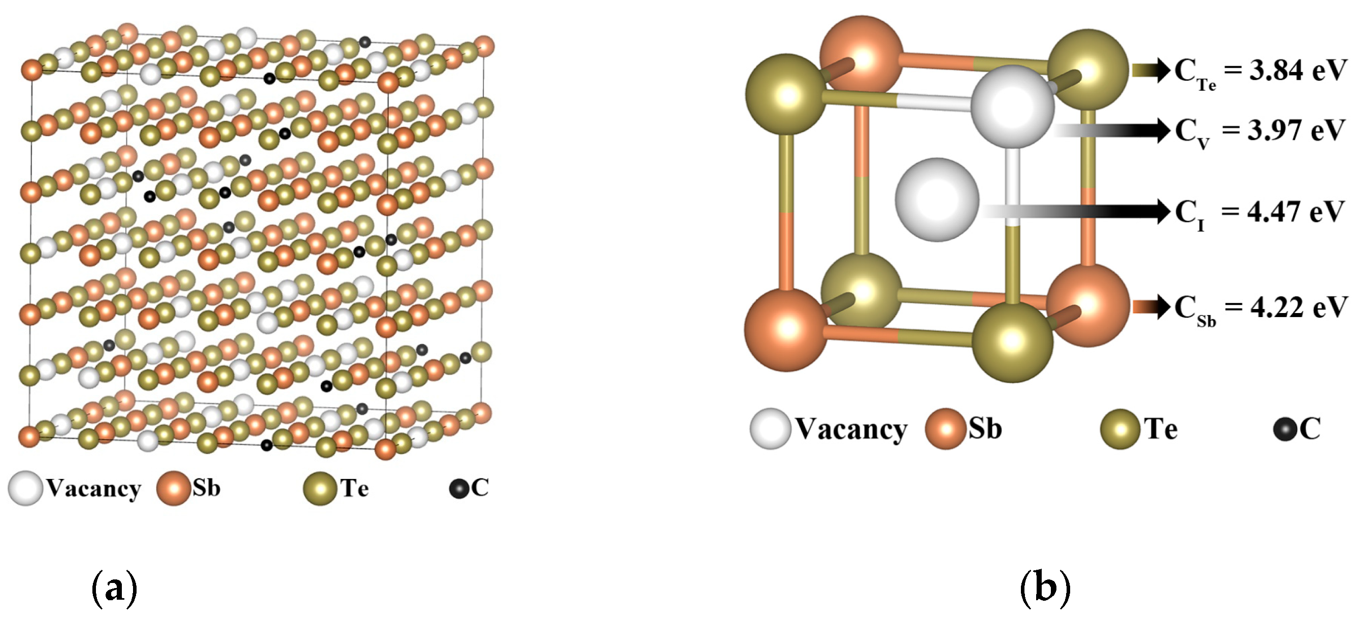
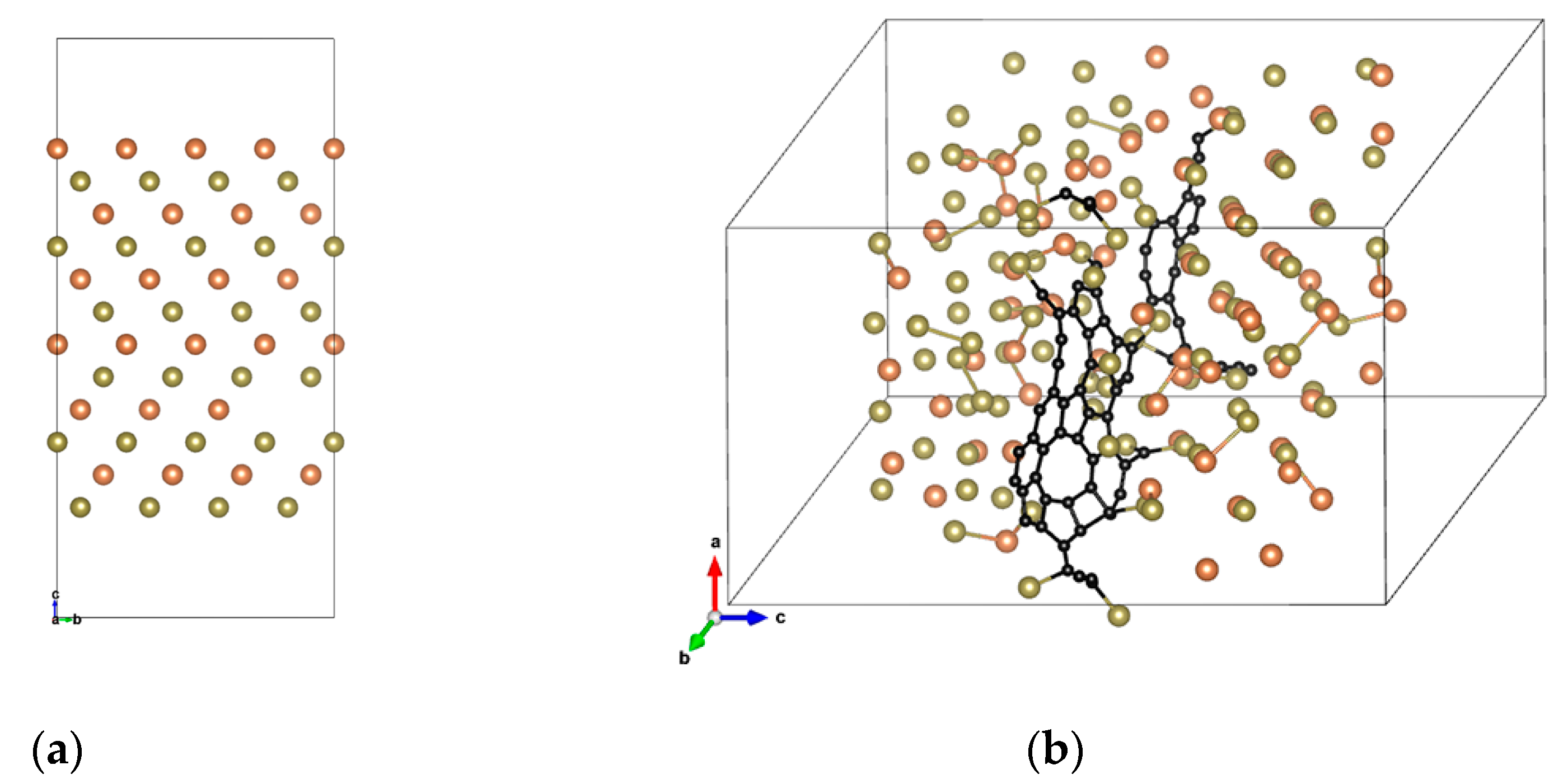
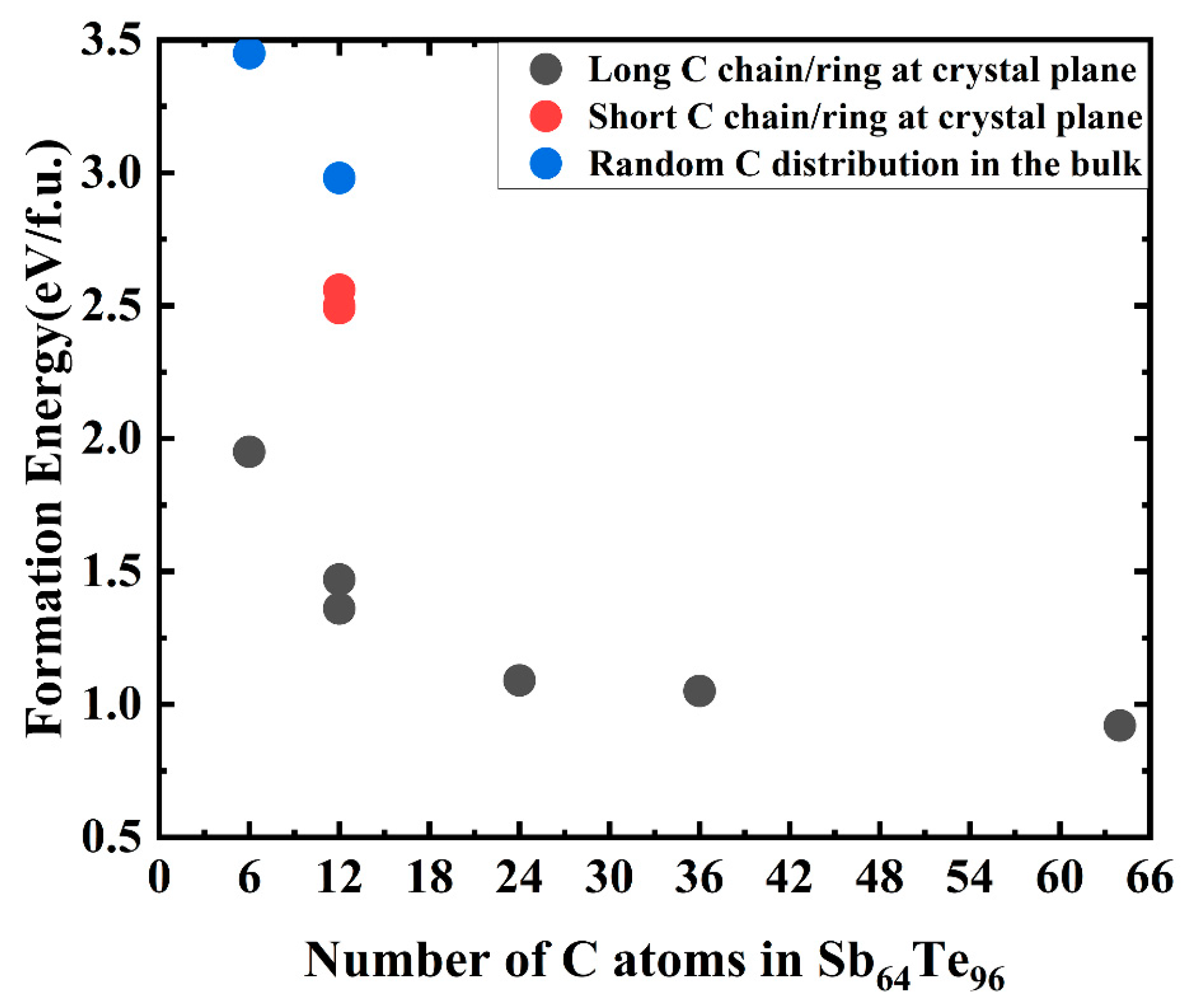
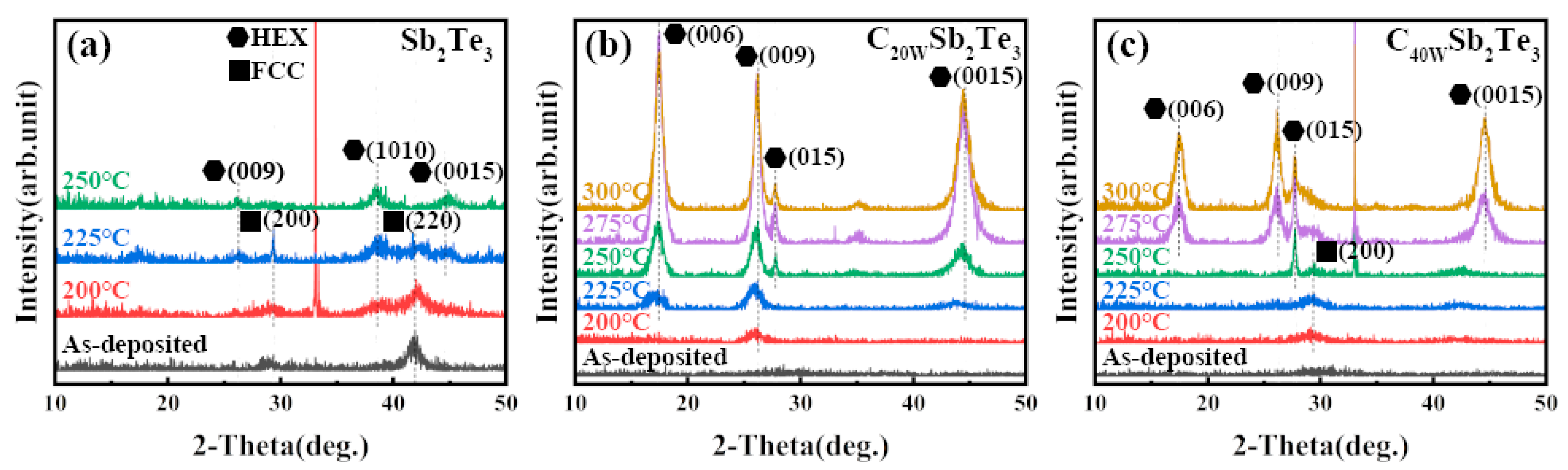
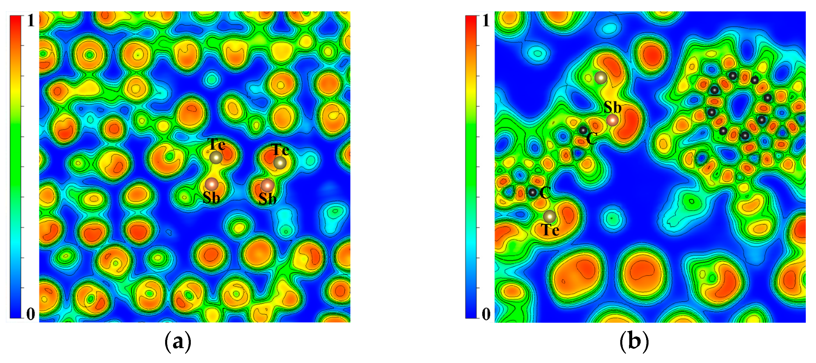
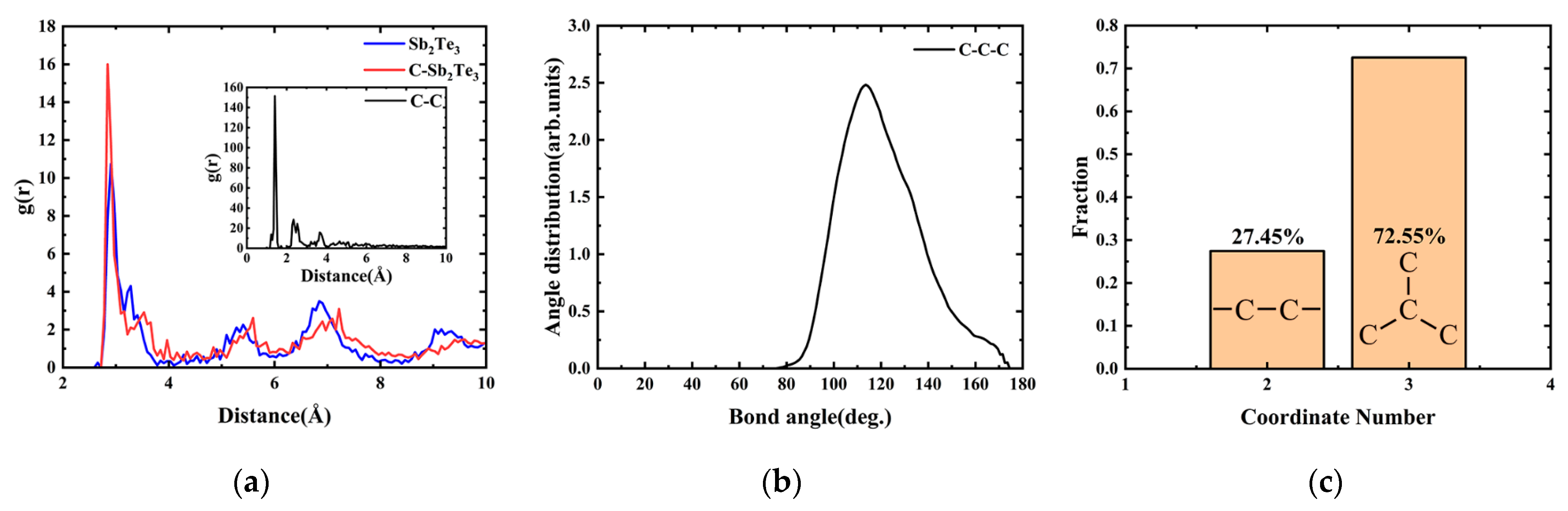
3.1. Atomic Configuration for C-Doped Sb2Te3

In order to determine the position of the C atom in Sb2Te3, we first consider four possible doping ways of the C atom in an FCC-Sb2Te3: replacing the Sb atom (CSb), replacing the Te atom (CTe), occupying Sb cation vacancy (CV), and interstitial doping (CI). On this basis, the formation energy of C doping in an FCC-Sb2Te3 was calculated and compared. The Equation for calculating the formation energy of C doping is as follows [15,20,21,25]:
E f [ X ] = E tot [ X ] E tot [ bulk ] i n i μ i ,
where E tot [ X ] and E tot [ bulk ] are the total energies of a supercell with and without C doping, respectively, and n i represents the number of doped atoms. n i > 0 means adding atoms to the supercell, n i < 0 means removing atoms from the supercell, and μ i means the chemical potential of i substance. In this paper, the chemical potentials of C, Sb, and Te are calculated according to the simple substance trigonal phase.
The FCC-Sb2Te3 supercell used in the calculation contains 36 cation vacancies, 72 Sb atoms, and 108 Te atoms. The FCC-Sb2Te3 model is shown in Figure 1a. The calculation results show that the formation energy of C atoms in every position of the FCC-Sb2Te3 is very high, as shown in Figure 1b, which indicates that the doping system is not easy to form or unstable; that is, the substitution/occupation position of C atoms is unreasonable.
It is found from the article [18,25,26,27,28] that C atoms are not simply doped in these four ways, but form C molecular clusters (such as C chain and/or C ring) on the crystal plane. The Σ3 twin grain boundary in an annealed C-Ge2Sb2Te5 alloy accounts for 7.49% of the total polycrystalline structure [28]. Figure 2a shows the FCC-Sb2Te3 with 160 atoms of Σ3 twin grain boundary, and the thickness of the vacuum layer in the c-axis direction is 10 Å.
After the structural relaxation, we found that the C atoms have a tendency to gradually converge together and form the C chain and/or C ring [29], as shown in Figure 2b. The longer the C chain, the more C rings, and the lower its formation energy. On the contrary, the more dispersed the C atom is, the higher its formation energy is. Figure 3 shows the formation energies of different C doping contents and forms calculated by Equation (1). As can be seen in Figure 3, comparing the formation energy of a single crystal structure (See Figure 1a) and a twin structure (See Figure 2a), the latter is lower, indicating that C atoms are more inclined to stay at the grain boundary than to replace Sb/Te atoms or occupy intervals/Sb cation vacancies in a single crystal. It is further analyzed that with the increase in C doping concentration, or with the increase in C chain and/or C ring, the formation energy of Sb2Te3 can gradually decrease, indicating that C atoms tend to converge to each other to form a C chain and/or C ring, which mainly exists in the form of a C chain and/or C ring at the twin grain boundary, as shown in Figure S1.
It can also be seen in Figure 3 that although the formation energy of C-Sb2Te3 gradually decreases with the increase in C doping concentration, its value is still greater than 0 (the formation energy of C64Sb64Te96 is 0.92 eV/f.u.), indicating that the structure is not easy to form or unstable. Perhaps this is the reason why the FCC structure was not found in the previous reports of Sb2Te3 doped with carbon, yet the hexagonal (HEX) structure was found. Yin et al. reported that there was no FCC structure in the experiment of C-doped Sb2Te3, but the FCC structure was observed in the experiment of N-doped Sb2Te3 [30] and C-N co-doped Sb2Te3 [31]. The samples of pure Sb2Te3 and Sb2Te3 films doped with different carbon contents were prepared, and their crystal structures were analyzed by XRD, as shown in Figure 4. It can be seen in Figure 4 that when Sb2Te3 is at 225 °C, the FCC phase and the HEX phase coexist, which indicates that Sb2Te3 starts to change from the FCC phase to the HEX phase at this time. In C40WSb2Te3, there is no HEX phase at 200 and 225 °C, but the characteristic peak of the FCC phase appears, and the transition from the FCC phase to the HEX phase begins at 250 °C. However, the characteristic peak of the FCC phase was not observed at 225–250 °C in C20WSb2Te3, which indicated that with the increase in C doping concentration, the formation energy of C-Sb2Te3 decreased, so that the FCC phase can appear in C-doped Sb2Te3, and the FCC phase is likely to be stable in the C-Sb2Te3 structure as the C concentration increases. The formation energy of the metastable FCC-Sb2Te3 structure constructed by us is calculated to be 0.04eV/f.u., which is close to kT = 0.026 eV at room temperature. However, the formation energy of the FCC-Sb2Te3 structure is greater than 0, which also indicates that its stability is poor. In order to further understand the chemical stability of the Sb2Te3 structure, we performed the COHP analysis for Sb2Te3, as shown in Figure 5. The upper and lower portions of the -COHP curve indicate bonding (stable) and anti-bonding (unstable) interactions, respectively. From the -COHP of Sb2Te3 in Figure 5, the existence of the anti-bonding state of Sb-Te atoms below Fermi level (Ef) also indicates that the stability of the FCC-Sb2Te3 structure is poor [32], where the cutoff distance of an Sb-Te bond is 3.1 Å [18,28,33,34]. Kolobov et al. theoretically predicted and constructed the structure model of the FCC-Sb2Te3 in 2013 [35], but it was not until 2016 that Zheng et al. observed the structure of the FCC-Sb2Te3 in the experiment for the first time using TEM analysis [34].

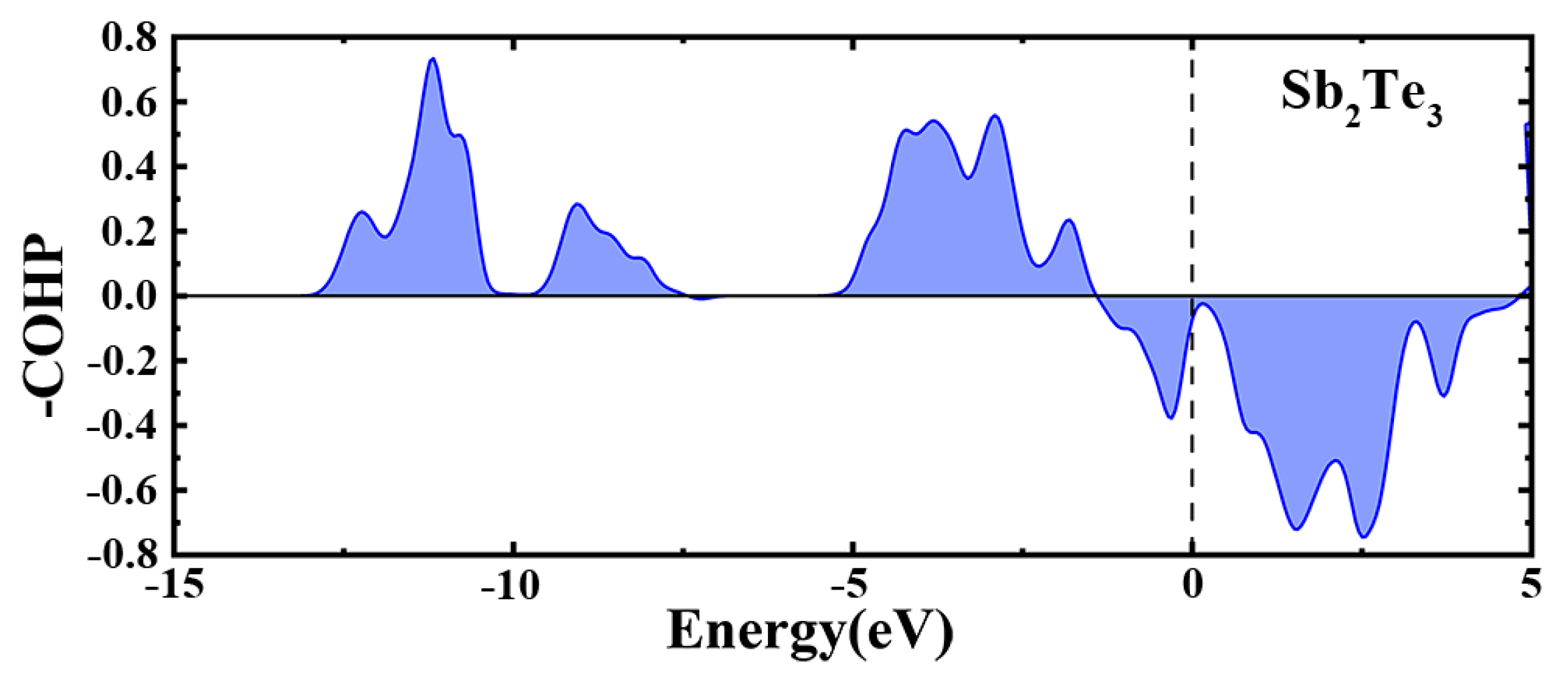
3.2. Electronic Properties and Origin of Change of Crystalline C-doped Sb2Te3

To understand the mechanism of the thermal stability improvement of C-doped Sb2Te3, contour plots of electron localization function (ELF) projected on the same planes for Sb2Te3 and 64C-Sb2Te3 are shown in Figure 6, and the ELF maxima of various bonds are shown in Table 1. It is shown that the ELF maximum of the C-C bond is much higher than that of other bonds, indicating that the strength of the C-C bond is very high, which also proves that C atoms mainly exist in the form of C molecular clusters in Sb2Te3. The ELF maximum values of C-Te and C-Sb bonds are obviously much higher than 0.5, which indicates that C-Te and C-Sb bonds have high strength; that is, there are some molecular clusters containing C-Te and C-Sb. In addition, it also shows that the doping of the C atoms changes the local environment of each element in Sb2Te3 and increases the strength of the Sb-Te covalent bond, thus obviously improving the stability of Sb2Te3 after C doping [36,37].
In order to represent the effect of C element doping on the amorphous thermal stability of Sb2Te3 materials, we tested the failure time of thin film materials at different temperatures. The failure time is considered to be that the film resistance drops to half of the initial resistance at this set temperature T. As shown in Figure 7, the 10-year (and 100-year) data retention is estimated according to the Arrhenius equation:
t = τ exp ( E a k b T ) ,
where t is the failure time of the film at a set temperature T, τ is the preexponential factor, Ea is the activation energy, and Kb is the Boltzmann constant. It can be seen in Figure 7 that the addition of C atoms obviously improves the 10-year (or 100-year) data retention of Sb2Te3.
Figure 8a shows the pair correlation function (PCF) of the C-C bond and the Sb-Te bond in crystal Sb2Te3 and C-Sb2Te3 after structural relaxation. For the first peak, we found that the peak value of the C-C bond is far greater than that of the Sb-Te bond, C-Sb bond, C-Te bond, etc., indicating that C atoms are more inclined to combine with C atoms in Sb2Te3 to form C molecular clusters. To our surprise, the position of the first peak of the C-C bond is 1.406 Å, which is very close to the inter-layer atomic spacing of 1.42 Å in graphite structure [38,39]. In addition, the maximum bond angle distribution of the C-C-C configuration in C molecular clusters is about 105–125°, and the coordination number of C atoms is mainly 3-coordinate, as shown in Figure 8b,c. These indicate that the doped C atoms in Sb2Te3 are not randomly formed when forming C molecular clusters, but tend to form graphite-like layered structures by sp2 hybridization [18,28]. The low PCF peaks of the C-Sb and C-Te bonds in Figure S2 indicate that C atoms bond less with Sb and Te atoms. It is observed that after doping the C atom in Sb2Te3, the position of the first peak value of the Sb-Te bond decreases and the bond length becomes shorter, indicating that the binding between Sb and Te atoms is strengthened, thus making the structure more stable. Meanwhile, the extremely unstable Sb-Sb homobonds are reduced, which also contributes to the enhancement of structural stability, as shown in Figure S2.

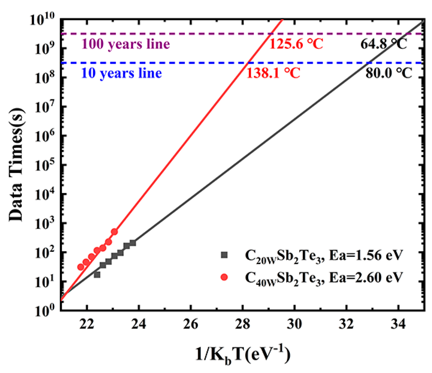
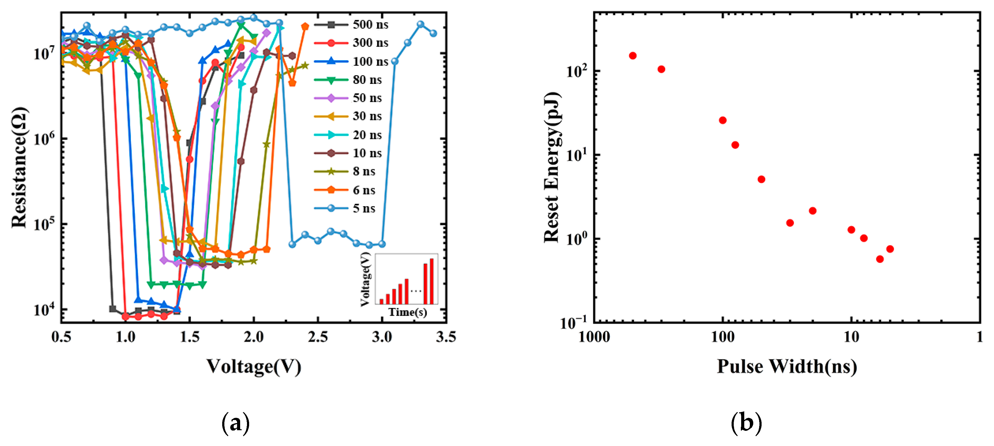
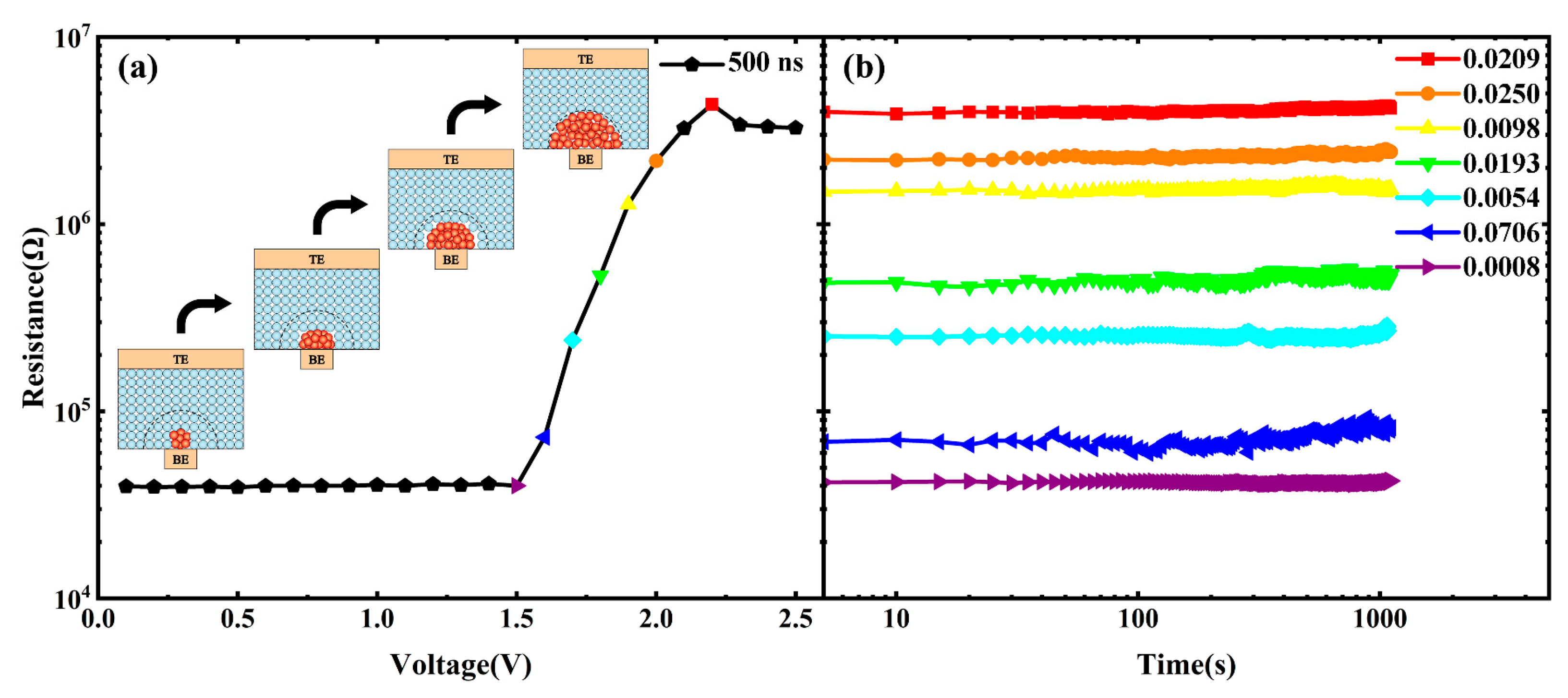
3.3. Electrical Performance Test of a Prototype PCRAM Device Based on C-Sb2Te3 Material

The electrical programming characteristics of the C-Sb2Te3 prototype PCRAM device are shown in Figure 9a. The illustration is the voltage pulse we applied to the PCRAM cell and the pulse width is fixed and the voltage amplitude step is set to 0.1 V. Starting from the first pulse amplitude of 0.1 V until the PCRAM cell stops after the SET and the RESET, as illustrated in Figure 9a, a reading voltage of 0.1 V is applied between every two pulses to record the resistance value of the PCRAM test cell. The initial state resistance value and the final state resistance value are controlled to be equal as much as possible. Obviously, the final state resistance value before adjusting the voltage pulse width is taken as the initial state resistance value after adjusting the voltage pulse width, and the initial state resistance value will affect the SET voltage value and even the RESET voltage value of this electrical programming. It can be seen from Figure 9a that the resistance resolution of the PCRAM cells exceeds two orders of magnitude, which meets the requirements of PCRAM. Our PCRAM device cells can be programmed at a very low SET/RESET voltage with a pulse width of 500 ns–5 ns, and the SET voltage and RESET voltage are as low as 1.5 V and 2.2 V when the voltage pulse width is 6 ns, which indicates that our PCRAM device has an operating speed of 5 ns and a low device power consumption (0.57 pJ), as shown in Figure 9b. Further observation in Figure 9b shows that the RESET power consumption of the PCRAM device cell decreases with the decrease in the width of the programming pulse. At the same time, it was noted that the PCRAM device cell could not be completely SET operated, as the width of the programming pulse decreased, resulting in the resistance value of its low resistance state to increase. This explains the behavior of the RESET power consumption change of the PCRAM device cell. However, the PCRAM device cell cannot be completely SET, which may be caused by the FCC phase appearing before the amorphous phase is transformed into the HEX phase due to the high C doping concentration. The multistage storage function can be realized by setting different voltage pulse widths and voltage pulse amplitudes, such as “0” at 107 Ω, “1” at 105 Ω, and “2” at 104 Ω [40]. We also noticed that during the SET/RESET process of our PCRAM device, there was a continuous resistance change. In this case, we used a voltage pulse with a pulse width of 500 ns to RESET the PCRAM in a low resistance state, and the continuously adjustable resistance value can be obtained as shown in Figure 10a. With this change, maybe we can realize several basic synaptic functions at the cell level, including long-term plasticity (LTP) [41,42], short-term plasticity (STP) [41,42], spike timing-dependent plasticity (STDP) [43,44], and spike rate-dependent plasticity (SRDP) [44,45], and maybe can also realize more complex or higher-order learning behaviors at the network level, such as supervised learning [46] and associative learning [47], as well as non-von Neumann architecture of in-memory computing [48,49]. In general, for this phenomenon of continuous resistance change, the resistance drift caused by the widening of the band gap due to the structural relaxation (SR) of amorphous Sb2Te3 is a great obstacle to multilevel storage, neuromorphic learning and in-memory computing. Li et al. greatly reduced this resistance drift phenomenon by bipolar pulse operation on the PCRAM cell [50], which provides an effective means to improve the stability of the phase-change neuromorphic applications. We adjusted the resistance values of the PCRAM cell to high and low resistance states and each intermediate resistance state by controlling the electrical signal applied to the PCRAM cell, and fitting the resistance drift coefficient by Equation (3):
R ( t ) = R 0 ( t t 0 ) ν ,
where R0 is the resistance value of the PCRAM cell at time t0; that is, the initial resistance. ν is the resistance drift coefficient, indicating the change in the resistance value of the PCRAM cell with time. The results measured at room temperature are shown in Figure 10b.

4. Conclusions

We have obtained an understanding of the doping position and existence form of C atoms in the FCC-Sb2Te3 and the improved device performance after C doping by performing density functional theory calculations for different concentrations and forms of C doping in single crystal FCC-Sb2Te3 and Σ3 twin boundary FCC-Sb2Te3. The results show that the formation energy of C-Sb2Te3 decreases with the increase in C doping concentration, which is consistent with the appearance of the FCC phase in high-concentration C-doped Sb2Te3 in our experiment. In addition, C atoms prefer to form C molecule clusters by sp2 hybridization at the grain boundary of Sb2Te3, similar to the layered structure of graphite, which changes the local environment of each element in Sb2Te3, resulting in the improvement of thermal stability of Sb2Te3. We fabricated the prototype device cells of PCRAM, which had an operating speed of 5 ns, a high thermal stability (10-year data retention temperature 138.1 °C), a low device power consumption of 0.57 pJ, and a resistance drift coefficient as low as 0.025, showing a continuously adjustable resistance. These performances all indicate that C-Sb2Te3-based PCRAM devices have great potential in applications, such as multilevel storage and spiking neural networks.

Supplementary Materials

The following supporting information can be downloaded at https://www.mdpi.com/article/10.3390/nano13040671/s1, Figure S1: After structural relaxation of different C doping contents and C existing forms; Figure S2: The pair correlation function after structure relaxation; Figure S3: XRD diagram of C40WSb2Te3 at 225 °C; Figure S4: The optical image of the fabricated PCRAM cells; Figure S5: I-V curve of PCRAM unit set from high resistance state to low resistance state by DC current; Figure S6: SET the PCRAM in a low resistance state with a large/small set pulse, and then RESET it with a 500 ns pulse to obtain a continuously adjustable resistance value.

Author Contributions

Conceptualization, L.W. and Z.S.; methodology, J.Z., L.W. and P.X.; software, validation, J.Z., Y.X., A.L., W.S. and Y.L.; formal analysis, J.Z.; investigation, J.Z. and N.R.; resources, L.W., Z.S. and S.S.; data curation, writing—original draft preparation, J.Z.; writing—review and editing, L.W., N.R. and A.L.; visualization, J.Z.; supervision, project administration, funding acquisition, L.W. and Z.S. All authors have read and agreed to the published version of the manuscript.

Funding

This research was funded by the National Natural Science Foundation of China (grant No. 61874151), the Science and Technology Council of Shanghai (grant. No. 19JC1416802, 22ZR1402200), and the Fundamental Research Funds for the Central Universities (grant. No. 2232022A-06).

Institutional Review Board Statement

Not applicable.

Informed Consent Statement

Not applicable.

Data Availability Statement

Not applicable.

Acknowledgments

The authors acknowledge the financial support from the State Key Laboratory of Functional Materials for Informatics, the Shanghai Institute of Microsystem and Information, the Chinese Academy of Sciences, and the College of Science, Donghua University.

Conflicts of Interest

The authors declare no conflict of interest.

References

  1. Fong, S.W.; Neumann, C.M.; Wong, H.S.P. Phase-Change Memory—Towards a Storage-Class Memory. IEEE Trans. Electron Devices 2017, 64, 4374–4385. [Google Scholar] [CrossRef]
  2. Wong, H.S.P.; Salahuddin, S. Memory leads the way to better computing. Nat. Nanotechnol. 2015, 10, 191–194. [Google Scholar] [CrossRef]
  3. Ung, G.M. Intel, Micron Announce New 3D XPoint Memory Type That’s 1,000 Times Faster than NAND, Really. Available online: https://www.pcworld.com/article/422680/intel-micron-announce-new-3dxpoint-memory-type-thats-1000-times-faster-than-nand.html (accessed on 1 March 2022).
  4. Rao, F.; Ding, K.; Zhou, Y.; Zheng, Y.; Xia, M.; Lv, S.; Song, Z.; Feng, S.; Ronneberger, I.; Mazzarello, R.; et al. Reducing the stochasticity of crystal nucleation to enable subnanosecond memory writing. Science 2017, 358, 1423–1427. [Google Scholar] [CrossRef] [PubMed]
  5. Zhao, J.; Yuan, Z.H.; Song, W.X.; Song, Z.T. High performance of Er-doped Sb2Te material used in phase change memory. J. Alloy. Compd. 2021, 889, 161701. [Google Scholar] [CrossRef]
  6. Zuliani, P.; Varesi, E.; Palumbo, E.; Borghi, M.; Tortorelli, I.; Erbetta, D.; Libera, G.D.; Pessina, N.; Gandolfo, A.; Prelini, C.; et al. Overcoming Temperature Limitations in Phase Change Memories With Optimized GexSbyTez. IEEE Trans. Electron Devices 2013, 60, 4020–4026. [Google Scholar] [CrossRef]
  7. Diaz Fattorini, A.; Cheze, C.; Lopez Garcia, I.; Petrucci, C.; Bertelli, M.; Righi Riva, F.; Prili, S.; Privitera, S.M.S.; Buscema, M.; Sciuto, A.; et al. Growth, Electronic and Electrical Characterization of Ge-Rich Ge-Sb-Te Alloy. Nanomaterials 2022, 12, 1340. [Google Scholar] [CrossRef]
  8. Xu, B.; Zhang, J.; Yu, G.; Ma, S.; Wang, Y.; Wang, Y. Thermoelectric properties of monolayer Sb2Te3. J. Appl. Phys. 2018, 124, 15104. [Google Scholar] [CrossRef]
  9. Verma, S.K.; Kandpal, K.; Kumar, P.; Kumar, A.; Wiemer, C. Performance of Topological Insulator (Sb2Te3)-Based Vertical Stacking Photodetector on n-Si Substrate. IEEE Trans. Electron Devices 2022, 69, 4342–4348. [Google Scholar] [CrossRef]
  10. Bryja, H.; Gerlach, J.W.; Prager, A.; Ehrhardt, M.; Rauschenbach, B.; Lotnyk, A. Epitaxial layered Sb2Te3 thin films for memory and neuromorphic applications. 2D Mater. 2021, 8, 045027. [Google Scholar] [CrossRef]
  11. Sun, Z.; Zhou, J.; Blomqvist, A.; Johansson, B.; Ahuja, R. Formation of large voids in the amorphous phase-change memory Ge2Sb2Te5 alloy. Phys. Rev. Lett. 2009, 102, 075504. [Google Scholar] [CrossRef]
  12. Li, L.; Song, S.N.; Xue, Y.; Chen, X.; Zhao, J.; Shen, J.B.; Song, Z.T. Thermally stable tungsten and titanium doped antimony tellurium films for phase change memory application. J. Mater. Sci.-Mater. Electron. 2020, 31, 10912–10918. [Google Scholar] [CrossRef]
  13. Ren, K.; Rao, F.; Song, Z.T.; Lv, S.L.; Cheng, Y.; Wu, L.C.; Peng, C.; Zhou, X.L.; Xia, M.J.; Liu, B.; et al. Pseudobinary Al2Te3-Sb2Te3 material for high speed phase change memory application. Appl. Phys. Lett. 2012, 100, 052105. [Google Scholar] [CrossRef]
  14. Zhang, T.; Zhang, K.; Wang, G.; Greenberg, E.; Prakapenka, V.B.; Yang, W.E. Multiple phase transitions in Sc doped Sb2Te3 amorphous nanocomposites under high pressure. Appl. Phys. Lett. 2020, 116, 021903. [Google Scholar] [CrossRef]
  15. Hu, S.W.; Liu, B.; Li, Z.; Zhou, J.; Sun, Z.M. Identifying optimal dopants for Sb2Te3 phase-change material by high-throughput ab initio calculations with experiments. Comput. Mater. Sci. 2019, 165, 51–58. [Google Scholar] [CrossRef]
  16. Zhu, M.; Wu, L.; Song, Z.; Rao, F.; Cai, D.; Peng, C.; Zhou, X.; Ren, K.; Song, S.; Liu, B.; et al. Ti10Sb60Te30 for phase change memory with high-temperature data retention and rapid crystallization speed. Appl. Phys. Lett. 2012, 100, 122101. [Google Scholar] [CrossRef]
  17. Cheng, Y.; Cai, D.; Zheng, Y.; Yan, S.; Wu, L.; Li, C.; Song, W.; Xin, T.; Lv, S.; Huang, R.; et al. Microscopic Mechanism of Carbon-Dopant Manipulating Device Performance in CGeSbTe-Based Phase Change Random Access Memory. ACS Appl. Mater. Interfaces 2020, 12, 23051–23059. [Google Scholar] [CrossRef]
  18. Zhou, X.; Xia, M.; Rao, F.; Wu, L.; Li, X.; Song, Z.; Feng, S.; Sun, H. Understanding phase-change behaviors of carbon-doped Ge2Sb2Te5 for phase-change memory application. ACS Appl. Mater. Interfaces 2014, 6, 14207–14214. [Google Scholar] [CrossRef]
  19. Sun, Z.; Zhou, J.; Mao, H.K.; Ahuja, R. Peierls distortion mediated reversible phase transition in GeTe under pressure. Proc. Natl. Acad. Sci. USA 2012, 109, 5948–5952. [Google Scholar] [CrossRef]
  20. Li, Z.; Si, C.; Zhou, J.; Xu, H.; Sun, Z. Yttrium-Doped Sb2Te3: A Promising Material for Phase-Change Memory. ACS Appl. Mater. Interfaces 2016, 8, 26126–26134. [Google Scholar] [CrossRef]
  21. Zhao, Z.Y.; Peng, S.; Tan, Z.L.; Wang, C.J.; Wen, M. Doping effects of Ru on Sb2Te and Sb2Te3 as phase change materials studied by first-principles calculations. Mater. Today Commun. 2022, 31, 103669. [Google Scholar] [CrossRef]
  22. Lee, T.H.; Elliott, S.R. The Relation between Chemical Bonding and Ultrafast Crystal Growth. Adv. Mater. 2017, 29, 1700814. [Google Scholar] [CrossRef] [PubMed]
  23. Lee, T.H.; Loke, D.; Elliott, S.R. Microscopic Mechanism of Doping-Induced Kinetically Constrained Crystallization in Phase-Change Materials. Adv. Mater. 2015, 27, 5477–5483. [Google Scholar] [CrossRef] [PubMed]
  24. Maintz, S.; Deringer, V.L.; Tchougréeff, A.L.; Dronskowski, R. Analytic projection from plane-wave and PAW wavefunctions and application to chemical-bonding analysis in solids. J. Comput. Chem. 2013, 34, 2557–2567. [Google Scholar] [CrossRef] [PubMed]
  25. Wang, G.J.; Zhou, J.; Elliott, S.R.; Sun, Z.M. Role of carbon-rings in polycrystalline GeSb2Te4 phase-change material. J. Alloy. Compd. 2019, 782, 852–858. [Google Scholar] [CrossRef]
  26. Zhou, X.; Wu, L.; Song, Z.; Rao, F.; Zhu, M.; Peng, C.; Yao, D.; Song, S.; Liu, B.; Feng, S. Carbon-doped Ge2Sb2Te5 phase change material: A candidate for high-density phase change memory application. Appl. Phys. Lett. 2012, 101, 142104. [Google Scholar] [CrossRef]
  27. Guo, T.; Song, S.; Zheng, Y.; Xue, Y.; Yan, S.; Liu, Y.; Li, T.; Liu, G.; Wang, Y.; Song, Z.; et al. Excellent thermal stability owing to Ge and C doping in Sb2Te-based high-speed phase-change memory. Nanotechnology 2018, 29, 505710. [Google Scholar] [CrossRef]
  28. Song, W.X.; Cheng, Y.; Cai, D.L.; Tang, Q.Y.; Song, Z.T.; Wang, L.H.; Zhao, J.; Xin, T.J.; Liu, Z.P. Improving the performance of phase-change memory by grain refinement. J. Appl. Phys. 2020, 128, 075101. [Google Scholar] [CrossRef]
  29. Zheng, L.; Song, W.X.; Zhang, S.F.; Song, Z.T.; Zhu, X.Q.; Song, S.N. Designing artificial carbon clusters using Ge2Sb2Te5/C superlattice-like structure for phase change applications. J. Alloy. Compd. 2021, 882, 160695. [Google Scholar] [CrossRef]
  30. Yin, Y.; Higano, N.; Ohta, K.; Miyachi, A.; Asai, M.; Niida, D.; Sone, H.; Hosaka, S. Characteristics of N-doped Sb2Te3 films by X-ray diffraction and resistance measurement for phase-change memory. In Proceedings of the Symposium on Materials and Processes for Nonvolatile Memories II Held at the 2007 MRS Spring Meeting, San Francisco, CA, USA, 10–13 April 2007; p. 287. [Google Scholar]
  31. Yin, Y. C–N-codoped Sb2Te3 chalcogenides for reducing writing current of phase-change devices. J. Appl. Phys. 2021, 117, 153502. [Google Scholar] [CrossRef]
  32. Zhao, J.; Song, W.X.; Xin, T.; Song, Z. Rules of hierarchical melt and coordinate bond to design crystallization in doped phase change materials. Nat. Commun. 2021, 12, 6473. [Google Scholar] [CrossRef]
  33. Sun, Z.; Zhou, J.; Pan, Y.; Song, Z.; Mao, H.K.; Ahuja, R. Pressure-induced reversible amorphization and an amorphous-amorphous transition in Ge2Sb2Te5 phase-change memory material. Proc. Natl. Acad. Sci. USA 2011, 108, 10410–10414. [Google Scholar] [CrossRef]
  34. Zheng, Y.; Xia, M.; Cheng, Y.; Rao, F.; Ding, K.; Liu, W.; Jia, Y.; Song, Z.; Feng, S. Direct observation of metastable face-centered cubic Sb2Te3 crystal. Nano Res. 2016, 9, 3453–3462. [Google Scholar] [CrossRef]
  35. Kolobov, A.V.; Fons, P.; Tominaga, J.; Ovshinsky, S.R. Vacancy-mediated three-center four-electron bonds in GeTe-Sb2Te3 phase-change memory alloys. Phys. Rev. B 2013, 87, 165206. [Google Scholar] [CrossRef]
  36. Zhou, W.Y.; Wu, L.C.; Zhou, X.L.; Rao, F.; Song, Z.T.; Yao, D.N.; Yin, W.J.; Song, S.N.; Liu, B.; Qian, B.; et al. High thermal stability and low density variation of carbon-doped Ge2Sb2Te5 for phase-change memory application. Appl. Phys. Lett. 2014, 105, 243113. [Google Scholar] [CrossRef]
  37. Li, T.; Shen, J.B.; Wu, L.C.; Song, Z.T.; Lv, S.L.; Cai, D.L.; Zhang, S.F.; Guo, T.Q.; Song, S.N.; Zhu, M. Atomic-Scale Observation of Carbon Distribution in High-Performance Carbon-Doped Ge2Sb2Te5 and Its Influence on Crystallization Behavior. J. Phys. Chem. C 2019, 123, 13377–13384. [Google Scholar] [CrossRef]
  38. Bernal, J.D. The structure of graphite. Proc. R. Soc. London. Ser. A Contain. Pap. A Math. Phys. Character 1924, 106, 749–773. [Google Scholar] [CrossRef]
  39. Chung, D. Review graphite. J. Mater. Sci. 2002, 37, 1475–1489. [Google Scholar] [CrossRef]
  40. Jin, S.M.; Kang, S.Y.; Kim, H.J.; Lee, J.Y.; Nam, I.H.; Shim, T.H.; Song, Y.H.; Park, J.G. Sputter-grown GeTe/Sb2Te3 superlattice interfacial phase change memory for low power and multi-level-cell operation. Electron. Lett. 2022, 58, 38–40. [Google Scholar] [CrossRef]
  41. Chee, M.Y.; Dananjaya, P.A.; Lim, G.J.; Du, Y.; Lew, W.S. Frequency-Dependent Synapse Weight Tuning in 1S1R with a Short-Term Plasticity TiOx-Based Exponential Selector. ACS Appl. Mater. Interfaces 2022, 14, 35959–35968. [Google Scholar] [CrossRef]
  42. Sarwat, S.G.; Kersting, B.; Moraitis, T.; Jonnalagadda, V.P.; Sebastian, A. Phase-change memtransistive synapses for mixed-plasticity neural computations. Nat. Nanotechnol. 2022, 17, 507–513. [Google Scholar] [CrossRef]
  43. Kuzum, D.; Jeyasingh, R.G.; Lee, B.; Wong, H.S. Nanoelectronic programmable synapses based on phase change materials for brain-inspired computing. Nano Lett. 2012, 12, 2179–2186. [Google Scholar] [CrossRef] [PubMed]
  44. Milo, V.; Pedretti, G.; Laudato, M.; Bricalli, A.; Ambrosi, E.; Bianchi, S.; Chicca, E.; Ielmini, D. Resistive switching synapses for unsupervised learning in feed-forward and recurrent neural networks. In Proceedings of the 2018 IEEE International Symposium on Circuits and Systems (ISCAS), Florence, Italy, 27–30 May 2018. [Google Scholar]
  45. Milo, V.; Pedretti, G.; Carboni, R.; Calderoni, A.; Ramaswamy, N.; Ambrogio, S.; Ielmini, D. A 4-Transistors/1-Resistor Hybrid Synapse Based on Resistive Switching Memory (RRAM) Capable of Spike-Rate-Dependent Plasticity (SRDP). IEEE Trans. Very Large Scale Integr. (VLSI) Syst. 2018, 26, 2806–2815. [Google Scholar] [CrossRef]
  46. Nandakumar, S.R.; Boybat, I.; Le Gallo, M.; Eleftheriou, E.; Sebastian, A.; Rajendran, B. Experimental Demonstration of Supervised Learning in Spiking Neural Networks with Phase-Change Memory Synapses. Sci. Rep. 2020, 10, 8080. [Google Scholar] [CrossRef] [PubMed]
  47. Cheng, Y.K.; Lin, Y.; Zeng, T.; Shan, X.Y.; Wang, Z.Q.; Zhao, X.N.; Ielmini, D.; Xu, H.Y.; Liu, Y.C. Pavlovian conditioning achieved via one-transistor/one-resistor memristive synapse. Appl. Phys. Lett. 2022, 120, 133503. [Google Scholar] [CrossRef]
  48. Sebastian, A.; Le Gallo, M.; Eleftheriou, E. Computational phase-change memory: Beyond von Neumann computing. J. Phys. D Appl. Phys. 2019, 52, 443002. [Google Scholar] [CrossRef]
  49. Wright, C.D.; Hosseini, P.; Diosdado, J.A.V. Beyond von-Neumann Computing with Nanoscale Phase-Change Memory Devices. Adv. Funct. Mater. 2012, 23, 2248–2254. [Google Scholar] [CrossRef]
  50. Li, X.; He, Q.; Tong, H.; Miao, X.S. Resistance Drift-Reduced Multilevel Storage and Neural Network Computing in Chalcogenide Phase Change Memories by Bipolar Operation. IEEE Electron Device Lett. 2022, 43, 565–568. [Google Scholar] [CrossRef]
Figure 1. (a) The FCC-Sb2Te3 model with 180 atoms and (b) C atoms replace/occupy the formation energies of Sb, Te atoms, Sb vacancies, and intervals in the FCC-Sb2Te3, respectively.
Nanomaterials 13 00671 g001
Figure 2. (a) The Σ3 twin grain boundary FCC-Sb2Te3 containing 160 atoms, and (b) the C atoms gradually converge at the crystal plane to form C molecular clusters.
Nanomaterials 13 00671 g002
Figure 3. The formation energy of the Sb2Te3 structure doped with different contents and different forms of C atoms/molecular clusters. The percentages of C atoms are 3.61%, 6.98%, 13.04%, 18.37%, and 28.57%, respectively.
Nanomaterials 13 00671 g003
Figure 4. An XRD diagram of Sb2Te3 and C-Sb2Te3 in the experiment. (a) Sb2Te3; (b) C20WSb2Te3; and (c) C40WSb2Te3 were annealed for 5 min at different temperatures in a N2 atmosphere.
Nanomaterials 13 00671 g004
Figure 5. The -COHP curve of Σ3 twin boundary FCC-Sb2Te3.
Nanomaterials 13 00671 g005
Figure 6. Two-dimensional electronic local function contour plots of Sb2Te3 and C-Sb2Te3. (a) Σ3 twin grain boundary FCC-Sb2Te3 without doping C atoms and (b) Σ3 twin grain boundary FCC-Sb2Te3-doped C atoms.
Nanomaterials 13 00671 g006
Figure 7. The 10-year (or 100-year) data retention temperature and activation energy of crystallization are deduced based on the Arrhenius equation, according to the failure time versus reciprocal temperature.
Nanomaterials 13 00671 g007
Figure 8. (a) Pair correlation function (PCF) of the Sb-Te bond and the C-C bond in crystal Sb2Te3 and C-Sb2Te3 after structural relaxation; (b) bond angle distribution of the C-C-C configuration; and (c) coordination number statistics of C atoms.
Nanomaterials 13 00671 g008
Figure 9. (a) The R-V electrical test of the prototype PCRAM device based on C-Sb2Te3 material, and (b) the relationship between power consumption and pulse width.
Nanomaterials 13 00671 g009
Figure 10. (a) The R-V curve is obtained by resetting the voltage pulse with a pulse width of 500 ns, and (b) the R-t curve and the resistance drift coefficient ν is obtained by fitting with Equation (2).
Nanomaterials 13 00671 g010
Table 1. The maximum electronic local function value of each covalent bond in the FCC-Sb2Te3 with Σ3 twin grain boundary of undoped/doped C atoms in the direction of bond length.
BondsSb2Te3C-Sb2Te3
Sb-Te0.780.80
C-C/0.94
C-Sb/0.91
C-Te/0.89
Disclaimer/Publisher’s Note: The statements, opinions and data contained in all publications are solely those of the individual author(s) and contributor(s) and not of MDPI and/or the editor(s). MDPI and/or the editor(s) disclaim responsibility for any injury to people or property resulting from any ideas, methods, instructions or products referred to in the content.

