
Highly Efficient and Stable Self-Powered Perovskite Photodiode by Cathode-Side Interfacial Passivation with Poly(Methyl Methacrylate)

 and
and 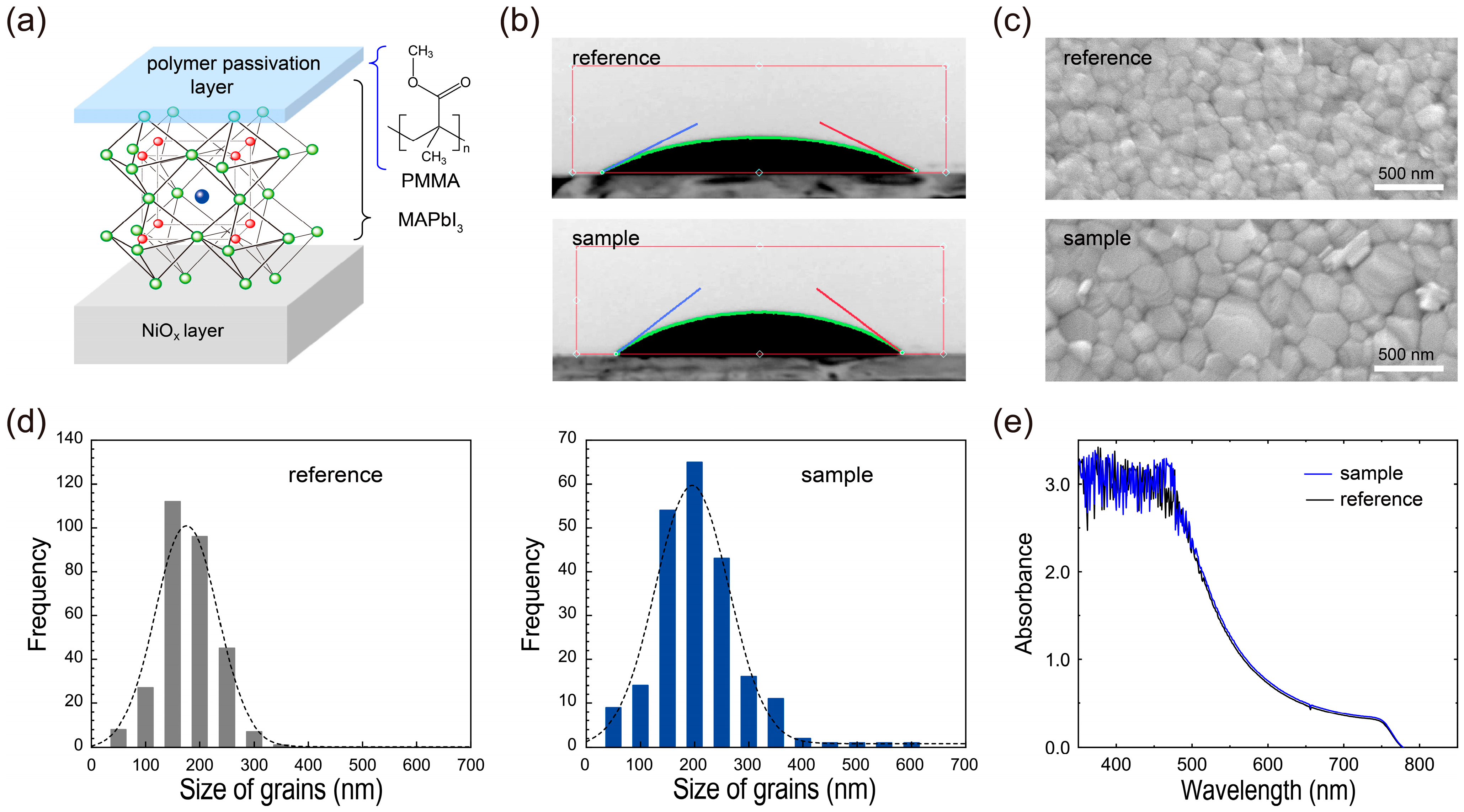
Abstract
:1. Introduction
2. Materials and Methods
2.1. Materials
2.2. Methods
2.3. Characterization
3. Results
3.1. Characteristics of MAPbI3 Layers with a PMMA Passivation Layer
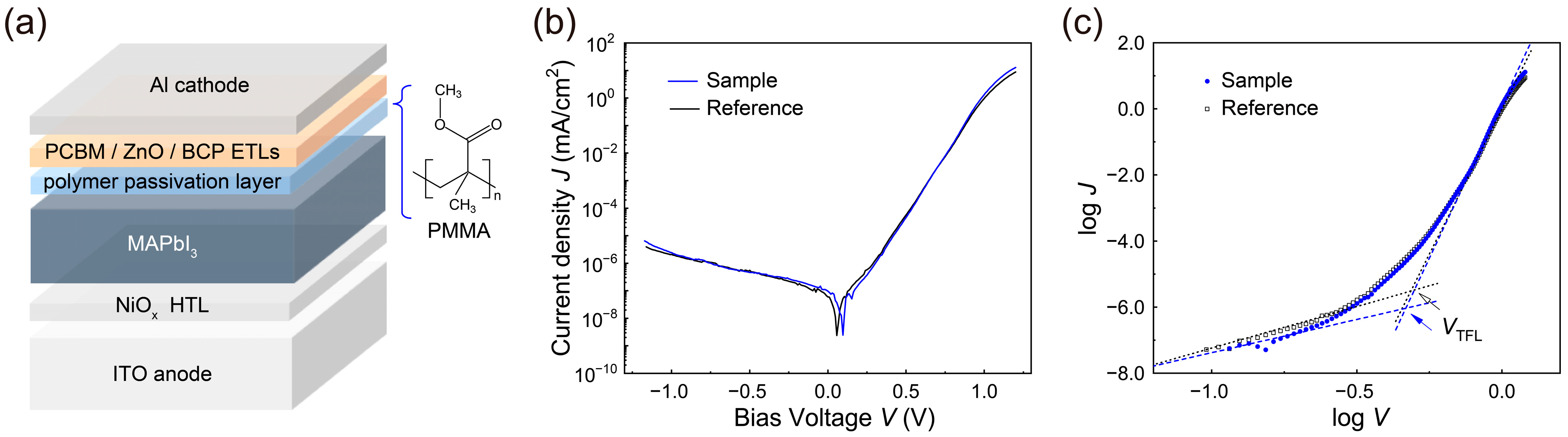
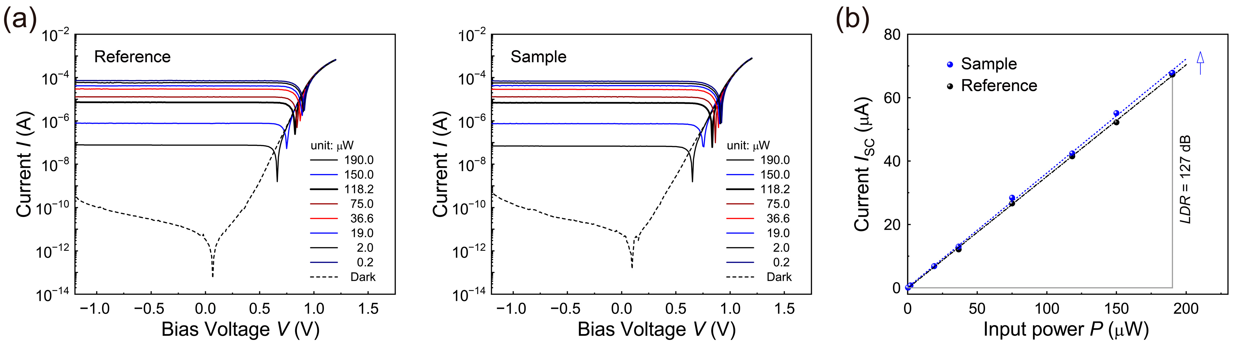
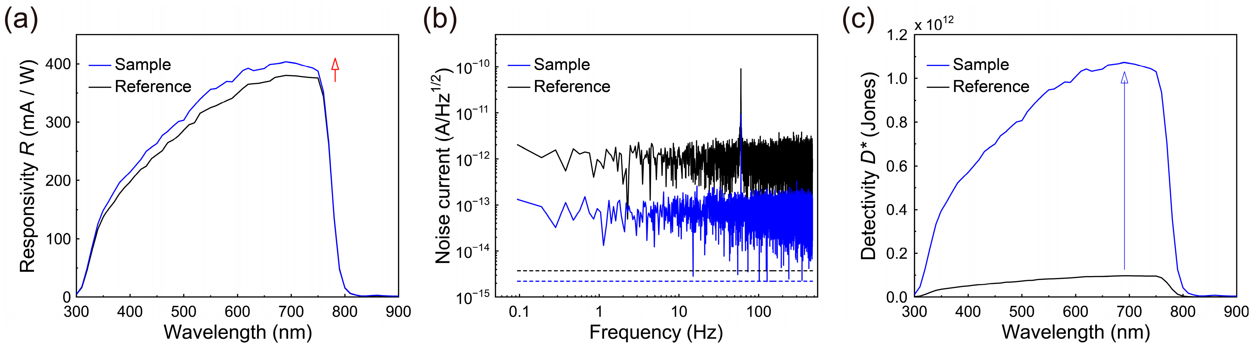
3.2. Characterization of Perovskite Photodiodes without and with a PMMA Passivation Layer
4. Discussion
5. Conclusions
Author Contributions
Funding
Institutional Review Board Statement
Informed Consent Statement
Data Availability Statement
Conflicts of Interest
References
- Kojima, A.; Teshima, K.; Shirai, Y.; Miyasaka, T. Organometal Halide Perovskites as Visible-Light Sensitizers for Photovoltaic Cells. J. Am. Chem. Soc. 2009, 131, 6050–6051. [Google Scholar] [CrossRef] [PubMed]
- Lee, M.M.; Teuscher, J.; Miyasaka, T.; Murakami, T.N.; Snaith, H.J. Efficient Hybrid Solar Cells based on Meso-Superstructured Organometal Halide Perovskites. Science 2012, 338, 643–647. [Google Scholar] [CrossRef] [PubMed]
- Bi, C.; Wang, Q.; Shao, Y.; Yuan, Y.; Xiao, Z.; Huang, J. Non-wetting Surface-Driven High-Aspect-Ratio Crystalline Grain Growth for Efficient Hybrid Perovskite Solar Cells. Nat. Commun. 2015, 6, 7747. [Google Scholar] [CrossRef] [PubMed]
- Momblona, C.; Gil-Escrig, L.; Bandiello, E.; Hutter, E.M.; Sessolo, M.; Lederer, K.; Blochwitz-Nimoth, J.; Bolink, H.J. Efficient Vacuum Deposited p-i-n and n-i-p Perovskite Solar Cells Employing Doped Charge Transport Layers. Energy Environ. Sci. 2016, 9, 3456–3463. [Google Scholar] [CrossRef]
- Eperon, G.E.; Leijtens, T.; Bush, K.A.; Prasanna, R.; Green, T.; Wang, J.T.-W.; McMeekin, D.P.; Volonakis, G.; Milot, R.L.; May, R.; et al. Perovskite-Perovskite Tandem Photovoltaics with Optimized Bandgaps. Science 2016, 354, 861–865. [Google Scholar] [CrossRef]
- Yang, W.S.; Park, B.-W.; Jung, E.H.; Jeon, N.J.; Kim, Y.C.; Lee, D.U.; Shin, S.S.; Seo, J.; Kim, E.K.; Noh, J.H.; et al. Iodide management in formamidinium-lead-halide-based perovskite layers for efficient solar cells. Science 2017, 356, 1376–1379. [Google Scholar] [CrossRef]
- Dou, L.; Yang, Y.M.; You, J.; Hong, Z.; Chang, W.-H.; Li, G.; Yang, Y. Solution-Processed Hybrid Perovskite Photodetectors with High Detectivity. Nat. Commun. 2014, 5, 5404. [Google Scholar] [CrossRef]
- Kwon, K.C.; Hong, K.; Van Le, Q.; Lee, S.Y.; Choi, J.; Kim, K.-B.; Kim, S.Y.; Jang, H.W. Inhibition of Ion Migration for Reliable Operation of Organolead Halide Perovskite-Based Metal/Semiconductor/Metal Broadband Photodetectors. Adv. Funct. Mater. 2016, 26, 4213–4222. [Google Scholar] [CrossRef]
- Veeramalai, C.P.; Feng, S.; Zhang, X.; Pammi, S.V.N.; Pecunia, V.; Li, C. Lead–halide Perovskites for Next-Generation Self-Powered Photodetectors: A Comprehensive Review. Photonics Res. 2021, 9, 968–991. [Google Scholar] [CrossRef]
- Shen, L.; Fang, Y.; Wang, D.; Bai, Y.; Deng, Y.; Wang, M.; Lu, Y.; Huang, J. A Self-Powered, Sub-nanosecond-Response Solution-Processed Hybrid Perovskite Photodetector for Time-Resolved Photoluminescence-Lifetime Detection. Adv. Mater. 2016, 28, 10794–10800. [Google Scholar] [CrossRef]
- Fang, Y.; Huang, J. Resolving Weak Light of Sub-picowatt per Square Centimeter by Hybrid Perovskite Photodetectors Enabled by Noise Reduction. Adv. Mater. 2015, 27, 2804–2810. [Google Scholar] [CrossRef]
- Zhao, Y.; Li, C.; Shen, L. Recent Advances on Organic-Inorganic Hybrid Perovskite Photodetectors with Fast Response. InfoMat 2019, 1, 164–182. [Google Scholar] [CrossRef]
- Afzal, A.M.; Bae, I.-G.; Aggarwal, Y.; Park, J.; Jeong, H.-R.; Choi, E.H.; Park, B. Highly Efficient Self-Powered Perovskite Photodiode with an Electron-Blocking Hole-Transport NiOx Layer. Sci. Rep. 2021, 11, 169. [Google Scholar] [CrossRef]
- Gong, X.; Tong, M.; Xia, Y.; Cai, W.; Moon, J.S.; Cao, Y.; Yu, G.; Shieh, C.-L.; Nilsson, B.; Heeger, A.J. High-Detectivity Polymer Photodetectors with Spectral Response from 300 nm to 1450 nm. Science 2009, 325, 1665–1667. [Google Scholar] [CrossRef]
- Son, D.-Y.; Lee, J.-W.; Choi, Y.J.; Jang, I.-H.; Lee, S.; Yoo, P.J.; Shin, H.; Ahn, N.; Choi, M.; Kim, D.; et al. Self-Formed Grain Boundary Healing Layer for Highly Efficient CH3NH3PbI3 Perovskite Solar Cells. Nat. Energy 2016, 1, 16081. [Google Scholar] [CrossRef]
- Bi, D.; Tress, W.; Dar, M.I.; Gao, P.; Luo, J.; Renevier, C.; Schenk, K.; Abate, A.; Giordano, F.; Baena, J.-P.C.; et al. Efficient Luminescent Solar Cells based on Tailored Mixed-Cation Perovskites. Sci. Adv. 2016, 2, e1501170. [Google Scholar] [CrossRef]
- Zheng, X.; Chen, B.; Dai, J.; Fang, Y.; Bai, Y.; Lin, Y.; Wei, H.; Zeng, X.C.; Huang, J. Defect Passivation in Hybrid Perovskite Solar Cells using Quaternary Ammonium Halide Anions and Cations. Nat. Energy 2017, 2, 17102. [Google Scholar] [CrossRef]
- Aydin, E.; De Bastiani, M.; De Wolf, S. Defect and Contact Passivation for Perovskite Solar Cells. Adv. Mater. 2019, 31, 1900428. [Google Scholar] [CrossRef]
- Cai, F.; Cai, J.; Yang, L.; Li, W.; Gurney, R.S.; Yi, H.; Iraqi, A.; Liu, D.; Wang, T. Molecular Engineering of Conjugated Polymers for Efficient Hole Transport and Defect Passivation in Perovskite Solar Cells. Nano Energy 2018, 45, 28–36. [Google Scholar] [CrossRef]
- Wang, D.; Xu, W.; Min, L.; Tian, W.; Li, L. Interfacial Passivation and Energy Level Alignment Regulation for Self-Powered Perovskite Photodetectors with Enhanced Performance and Stability. Adv. Mater. Interfaces 2022, 9, 2101766. [Google Scholar] [CrossRef]
- Wang, C.; Liu, M.; Rahman, S.; Pasanen, H.P.; Tian, J.; Li, J.; Deng, Z.; Zhang, H.; Vivo, P. Hydrogen Bonding Drives the self-Assembling of Carbazole-Based Hole-Transport Material for Enhanced Efficiency and Stability of Perovskite Solar Cells. Nano Energy 2022, 101, 107604. [Google Scholar] [CrossRef]
- Li, R.; Liu, M.; Matta, S.K.; Hiltunen, A.; Deng, Z.; Wang, C.; Dai, Z.; Russo, S.P.; Vivo, P.; Zhang, H. Sulfonated Dopant-Free Hole-Transport Material Promotes Interfacial Charge Transfer Dynamics for Highly Stable Perovskite Solar Cells. Adv. Sustain. Syst. 2021, 5, 2100244. [Google Scholar] [CrossRef]
- Piao, C.; Xi, J.; Choi, M. Directionally Selective Polyhalide Molecular Glue for Stable Inverted Perovskite Solar Cells. Sol. RRL 2020, 4, 2000244. [Google Scholar] [CrossRef]
- Kim, M.; Motti, S.G.; Sorrentino, R.; Petrozza, A. Enhanced Solar Cell Stability by Hygroscopic Polymer Passivation of Metal Halide Perovskite Thin Film. Energy Environ. Sci. 2018, 11, 2609–2619. [Google Scholar] [CrossRef]
- Park, J.; Aggarwal, Y.; Kim, W.; Sharma, S.; Choi, E.H.; Park, B. Self-powered CH3NH3PbI3 Perovskite Photodiode with a Noise-Suppressible Passivation Layer of Poly(Methyl Methacrylate). Opt. Express 2023, 31, 1202–1213. [Google Scholar] [CrossRef]
- Frolova, L.A.; Davlethanov, A.I.; Dremova, N.N.; Zhidkov, I.; Akbulatov, A.F.; Kurmaev, E.Z.; Aldoshin, S.M.; Stevenson, K.J.; Troshin, P.A. Efficient and Stable MAPbI3-Based Perovskite Solar Cells using Polyvinylcarbazole Passivation. J. Phys. Chem. Lett. 2020, 11, 6772–6778. [Google Scholar] [CrossRef]
- Du, Y.; Xin, C.; Huang, W.; Shi, B.; Ding, Y.; Wei, C.; Zhao, Y.; Li, Y.; Zhang, X. Polymeric Surface Modification of NiOx-Based Inverted Planar Perovskite Solar Cells with Enhanced Performance. ACS Sustain. Chem. Eng. 2018, 6, 16806–16812. [Google Scholar] [CrossRef]
- Shi, Y.-R.; Wang, K.-L.; Lou, Y.-H.; Zhang, D.-B.; Chen, C.-H.; Chen, J.; Ni, Y.-X.; Öz, S.; Wang, Z.-K.; Liao, L.-S. Unraveling the Role of Active Hydrogen Caused by Carbonyl Groups in Surface-Defect Passivation of Perovskite Photovoltaics. Nano Energy 2022, 97, 107200. [Google Scholar] [CrossRef]
- Cai, Y.; Cui, J.; Chen, M.; Zhang, M.; Han, Y.; Qian, F.; Zhao, H.; Yang, S.; Yang, Z.; Bian, H.; et al. Multifunctional Enhancement for Highly Stable and Efficient Perovskite Solar Cells. Adv. Funct. Mater. 2021, 31, 2005776. [Google Scholar] [CrossRef]
- Lin, Y.; Shen, L.; Dai, J.; Deng, Y.; Wu, Y.; Bai, Y.; Zheng, X.; Wang, J.; Fang, Y.; Wei, H. π-Conjugated Lewis Base: Efficient Trap-Passivation and Charge-Extraction for Hybrid Perovskite Solar Cells. Adv. Mater. 2017, 29, 1604545. [Google Scholar] [CrossRef]
- Taguchi, M.; Suzuki, A.; Ueoka, N.; Oku, T. Effects of poly(Methyl Methacrylate) Addition to Perovskite Photovoltaic Devices. AIP Conf. Proc. 2019, 2067, 020018. [Google Scholar]
- Jo, B.; Han, G.S.; Yu, H.M.; Choi, J.; Zhu, J.; Ahn, T.K.; Namkoong, G.; Jung, H.S. Composites of Cross-Linked Perovskite/Polymer with Sodium Borate for Efficient and Stable Perovskite Solar Cells. J. Mater. Chem. A 2022, 10, 14884–14893. [Google Scholar] [CrossRef]
- Ochoa-Martinez, E.; Ochoa, M.; Ortuso, R.D.; Ferdowsi, P.; Carron, R.; Tiwari, A.N.; Steiner, U.; Saliba, M. Physical Passivation of Grain Boundaries and Defects in Perovskite Solar Cells by an Isolating Thin Polymer. ACS Energy Lett. 2021, 6, 2626–2634. [Google Scholar] [CrossRef]
- Peng, J.; Khan, J.I.; Liu, W.; Ugur, E.; Duong, T.; Wu, Y.; Shen, H.; Wang, K.; Dang, H.; Aydin, E.; et al. A Universal Double-Side Passivation for High Open-Circuit Voltage in Perovskite Solar Cells: Role of Carbonyl Groups in Poly(methyl methacrylate). Adv. Energy Mater. 2018, 8, 1801208. [Google Scholar] [CrossRef]
- Yang, F.; Lim, H.E.; Wang, F.; Ozaki, M.; Shimazaki, A.; Liu, J.; Mohamed, N.B.; Shinokita, K.; Miyauchi, Y.; Wakamiya, A.; et al. Roles of Polymer Layer in Enhanced Photovoltaic Performance of Perovskite Solar Cells via Interface Engineering. Adv. Mater. Interfaces 2018, 5, 1701256. [Google Scholar] [CrossRef]
- Kim, H.; Lee, K.S.; Paik, M.J.; Lee, D.Y.; Lee, S.-U.; Choi, E.; Yun, J.S.; Seok, S.I. Polymethyl Methacrylate as an Interlayer Between the Halide Perovskite and Copper Phthalocyanine Layers for Stable and Efficient Perovskite Solar Cells. Adv. Funct. Mater. 2022, 32, 2110473. [Google Scholar] [CrossRef]
- Choi, K.; Choi, H.; Min, J.; Kim, T.; Kim, D.; Son, S.Y.; Kim, G.-W.; Choi, J.; Park, T. A Short Review on Interface Engineering of Perovskite Solar Cells: A Self-Assembled Monolayer and Its Roles. Sol. RRL 2020, 4, 1900251. [Google Scholar] [CrossRef]
- Bube, R.H. Trap Density Determination by Space-Charge-Limited Currents. J. Appl. Phys. 1962, 33, 1733–1737. [Google Scholar] [CrossRef]
- Sworakowski, J.; Ferreira, G.F.L. Space-Charge-Limited Currents and Trap-Filled Limit in One-Dimensional Insulators. J. Phys. D Appl. Phys. 1984, 17, 135. [Google Scholar] [CrossRef]
- Speirs, M.J.; Dirin, D.N.; Abdu-Aguye, M.; Balazs, D.M.; Kovalenko, M.V.; Loi, M.A. Temperature Dependent Behaviour of Lead Sulfide Quantum Dot Solar Cells and Films. Energy Environ. Sci. 2016, 9, 2916–2924. [Google Scholar] [CrossRef]
- Ryu, S.; Nguyen, D.C.; Ha, N.Y.; Park, H.J.; Ahn, Y.H.; Park, J.-Y.; Lee, S. Light Intensity-dependent Variation in Defect Contributions to Charge Transport and Recombination in a Planar MAPbI3 Perovskite Solar Cell. Sci. Rep. 2019, 9, 19846. [Google Scholar] [CrossRef] [PubMed] [Green Version]
- Cao, Q.; Li, Y.; Zhang, H.; Yang, J.; Han, J.; Xu, T.; Wang, S.; Wang, Z.; Gao, B.; Zhao, J.; et al. Efficient and Stable Inverted Perovskite Solar Cells with Very High Fill Factors via Incorporation of Star-Shaped Polymer. Sci. Adv. 2021, 7, eabg0633. [Google Scholar] [CrossRef] [PubMed]
- Lu, H.; Tian, W.; Cao, F.; Ma, Y.; Gu, B.; Li, L. A Self-Powered and Stable All-Perovskite Photodetector–Solar Cell Nanosystem. Adv. Funct. Mater. 2016, 26, 1296–1302. [Google Scholar] [CrossRef]
- Xue, J.; Zhu, Z.; Xu, X.; Gu, Y.; Wang, S.; Xu, L.; Zou, Y.; Song, J.; Zeng, H.; Chen, Q. Narrowband Perovskite Photodetector-Based Image Array for Potential Application in Artificial Vision. Nano Lett. 2018, 18, 7628–7634. [Google Scholar] [CrossRef] [PubMed]
- Li, C.; Wang, H.; Wang, F.; Li, T.; Xu, M.; Wang, H.; Wang, Z.; Zhan, X.; Hu, W.; Shen, L. Ultrafast and broadband photodetectors based on a perovskite/organic bulk heterojunction for large-dynamic-range imaging. Light: Sci. Appl. 2020, 9, 31. [Google Scholar] [CrossRef]
- Wang, Y.; Liu, Y.; Cao, S.; Wang, J. A Review on Solution-Processed Perovskite/Organic Hybrid Photodetectors. J. Mater. Chem. C 2021, 9, 5302–5322. [Google Scholar] [CrossRef]
- Guo, F.; Yang, B.; Yuan, Y.; Xiao, Z.; Dong, Q.; Bi, Y.; Huang, J. A Nanocomposite Ultraviolet Photodetector Based on Interfacial Trap-Controlled Charge Injection. Nat. Nanotechnol. 2012, 7, 798–802. [Google Scholar] [CrossRef]
- Li, T.; Li, Q.; Tang, X.; Chen, Z.; Li, Y.; Zhao, H.; Wang, S.; Ding, X.; Zhang, Y.; Yao, J. Environment-Friendly Antisolvent Tert-Amyl Alcohol Modified Hybrid Perovskite Photodetector with High Responsivity. Photonics Res. 2021, 9, 781–791. [Google Scholar] [CrossRef]
- Wang, S.; Li, T.; Li, Q.; Zhao, H.; Zheng, C.; Li, M.; Li, J.; Zhang, Y.; Yao, J. Inhibition of Buried Cavities and Defects in Metal Halide Perovskite Photodetectors via a Two-Step Spin-Coating Method. J. Mater. Chem. C 2022, 10, 7886–7895. [Google Scholar] [CrossRef]
- Ma, N.; Jiang, J.; Zhao, Y.; He, L.; Ma, Y.; Wang, H.; Zhang, L.; Shan, C.; Shen, L.; Hu, W. Stable and Sensitive Tin-Lead Perovskite Photodetectors Enabled by Azobenzene Derivative for Near-Infrared Acousto-Optic Conversion Communications. Nano Energy 2021, 86, 106113. [Google Scholar] [CrossRef]


Disclaimer/Publisher’s Note: The statements, opinions and data contained in all publications are solely those of the individual author(s) and contributor(s) and not of MDPI and/or the editor(s). MDPI and/or the editor(s) disclaim responsibility for any injury to people or property resulting from any ideas, methods, instructions or products referred to in the content. |
© 2023 by the authors. Licensee MDPI, Basel, Switzerland. This article is an open access article distributed under the terms and conditions of the Creative Commons Attribution (CC BY) license (https://creativecommons.org/licenses/by/4.0/).
Share and Cite
Kim, W.; Park, J.; Aggarwal, Y.; Sharma, S.; Choi, E.H.; Park, B. Highly Efficient and Stable Self-Powered Perovskite Photodiode by Cathode-Side Interfacial Passivation with Poly(Methyl Methacrylate). Nanomaterials 2023, 13, 619. https://doi.org/10.3390/nano13030619
Kim W, Park J, Aggarwal Y, Sharma S, Choi EH, Park B. Highly Efficient and Stable Self-Powered Perovskite Photodiode by Cathode-Side Interfacial Passivation with Poly(Methyl Methacrylate). Nanomaterials. 2023; 13(3):619. https://doi.org/10.3390/nano13030619
Chicago/Turabian StyleKim, Wonsun, JaeWoo Park, Yushika Aggarwal, Shital Sharma, Eun Ha Choi, and Byoungchoo Park. 2023. "Highly Efficient and Stable Self-Powered Perovskite Photodiode by Cathode-Side Interfacial Passivation with Poly(Methyl Methacrylate)" Nanomaterials 13, no. 3: 619. https://doi.org/10.3390/nano13030619