
Control of the Nanopore Architecture of Anodic Alumina via Stepwise Anodization with Voltage Modulation and Pore Widening

Abstract
:1. Introduction
2. Materials and Methods
2.1. Electropolishing
2.2. Pre-Patterning
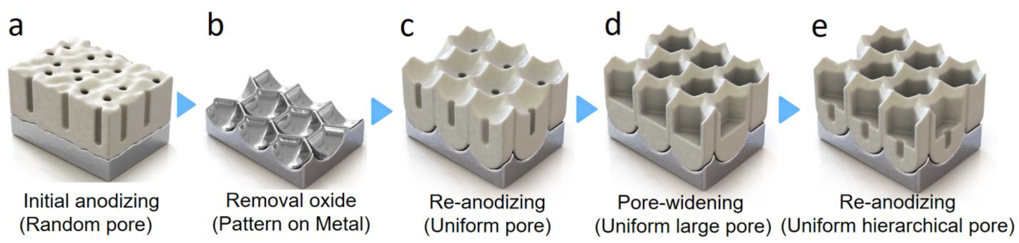
2.3. Stepwise Anodizing
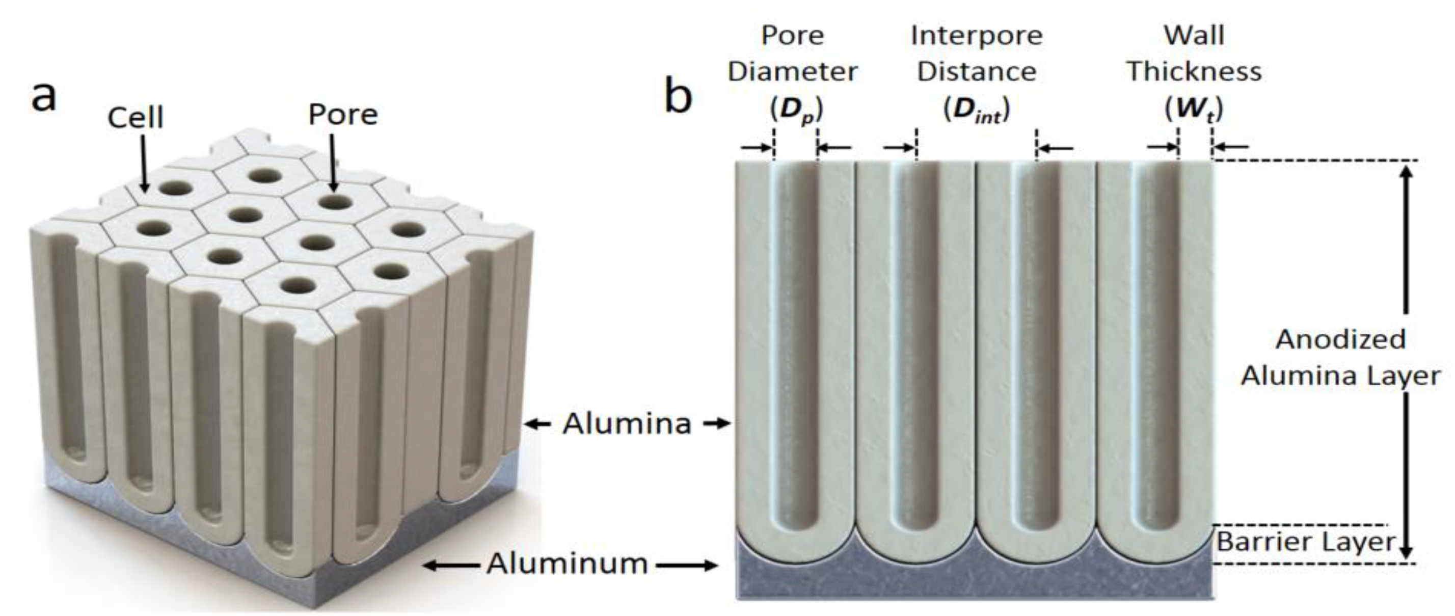
2.4. Characterization of Nanopore Morphology
3. Results
3.1. Effect of Voltage Modulation on Electropolished Aluminum Substrate
3.2. Effect of Voltage Modulation on Pre-Patterned Aluminum Substrate
3.3. Effects of PW Time on the Stepwise Anodizing Process
4. Conclusions
Author Contributions
Funding
Institutional Review Board Statement
Informed Consent Statement
Data Availability Statement
Conflicts of Interest
References
- Keller, F.; Hunter, M.S.; Robinson, D.L. Structural features of oxide coatings on aluminum. J. Electrochem. Soc. 1953, 100, 411–419. [Google Scholar] [CrossRef]
- Jeong, C.; Choi, C.-H. Single-step direct fabrication of pillar-on-pore hybrid nanostructures in anodizing aluminum for superior superhydrophobic efficiency. ACS Appl. Mater. Interfaces 2012, 4, 842–848. [Google Scholar] [CrossRef] [PubMed]
- Kim, S.H.; Jeong, C. Feasibility of machine learning algorithms for predicting the deformation of anodic titanium films by modulating anodization processes. Materials 2021, 14, 1089. [Google Scholar] [CrossRef]
- Masuda, H.; Fukuda, K. Ordered metal nanohole arrays made by a two-step replication of honeycomb structures of anodic alumina. Science 1995, 268, 1466–1468. [Google Scholar] [CrossRef] [PubMed]
- Li, A.P.; Muller, F.; Birner, A.; Nielsch, K.; Gosele, U. Hexagonal pore arrays with a 50–420 nm interpore distance formed by self-organization in anodic alumina. J. Appl. Phys. 1998, 84, 6023–6026. [Google Scholar] [CrossRef] [Green Version]
- Chu, S.Z.; Wada, K.; Inoue, S.; Isogai, M.; Yasumori, A. Fabrication of ideally ordered nanoporous alumina films and integrated alumina nanotubule arrays by high-field anodization. Adv. Mater. 2005, 17, 2115–2119. [Google Scholar] [CrossRef]
- Lee, W.; Ji, R.; Gosele, U.; Nielsch, K. Fast fabrication of long-range ordered porous alumina membranes by hard anodization. Nat. Mater. 2006, 5, 741–747. [Google Scholar] [CrossRef] [PubMed]
- Mortazavi, N.; Geers, C.; Esmaily, M.; Babic, V.; Sattari, M.; Lindgren, K.; Malmberg, P.; Jonsson, B.; Halvarsson, M.; Svensson, J.E.; et al. Interplay of water and reactive elements in oxidation of alumina-forming alloys. Nat. Mater. 2018, 17, 610–617. [Google Scholar] [CrossRef]
- Masuda, H.; Yada, K.; Osaka, A. Self-ordering of cell configuration of anodic porous alumina with large-size pores in phosphoric acid solution. Jpn. J. Appl. Phys. 1998, 37, L1340–L1342. [Google Scholar] [CrossRef]
- Ono, S.; Saito, M.; Asoh, H. Self-ordering of anodic porous alumina formed in organic acid electrolytes. Electrochim. Acta 2005, 51, 827–833. [Google Scholar] [CrossRef]
- Su, Z.; Zhou, W. Pore diameter control in anodic titanium and aluminium oxides. J. Mater. Chem. 2011, 21, 357–362. [Google Scholar] [CrossRef]
- Evertsson, J.; Vinogradov, N.A.; Harlow, G.S.; Carla, F.; McKibbin, S.R.; Rullik, L.; Linpe, W.; Felici, R.; Lundgren, E. Self-organization of porous anodic alumina films studied in situ by grazing-incidence transmission small-angle x-ray scattering. RSC Adv. 2018, 8, 18980–18991. [Google Scholar] [CrossRef] [Green Version]
- Haberkorn, N.; Gutmann, J.S.; Theato, P. Template-assisted fabrication of free-standing nanorod arrays of a hole-conducting cross-linked triphenylamine derivative: Toward ordered bulk-heterojunction solar cells. ACS Nano 2009, 3, 1415–1422. [Google Scholar] [CrossRef] [PubMed]
- Holtz, J.H.; Asher, S.A. Polymerized colloidal crystal hydrogel films as intelligent chemical sensing materials. Nature 1997, 389, 829–832. [Google Scholar] [CrossRef] [PubMed]
- Deubel, M.; von Freymann, G.; Wegener, M.; Pereira, S.; Busch, K.; Soukoulis, C.M. Direct laser writing of three-dimensional photonic-crystal templates for telecommunications. Nat. Mater. 2004, 3, 444–447. [Google Scholar] [CrossRef]
- Choudhari, K.S.; Choi, C.H.; Chidangil, S.; George, S.D. Recent progress in the fabrication and optical properties of nanoporous anodic alumina. Nanomaterials 2022, 12, 444. [Google Scholar] [CrossRef] [PubMed]
- Sauer, G.; Brehm, G.; Schneider, S.; Nielsch, K.; Wehrspohn, R.B.; Choi, J.; Hofmeister, H.; Gosele, U. Highly ordered monocrystalline silver nanowire arrays. J. Appl. Phys. 2002, 91, 3243–3247. [Google Scholar] [CrossRef]
- Choi, J.; Sauer, G.; Nielsch, K.; Wehrspohn, R.B.; Gosele, U. Hexagonally arranged monodisperse silver nanowires with adjustable diameter and high aspect ratio. Chem. Mater. 2003, 15, 776–779. [Google Scholar] [CrossRef]
- Zhang, F.; Zhao, L.; Chen, H.; Xu, S.; Evans, D.G.; Duan, X. Corrosion resistance of superhydrophobic layered double hydroxide films on aluminum. Angew. Chem. Int. Ed. 2008, 47, 2466–2469. [Google Scholar] [CrossRef]
- Jeong, C.; Lee, J.; Sheppard, K.; Choi, C.-H. Air-impregnated nanoporous anodic aluminum oxide layers for enhancing the corrosion resistance of aluminum. Langmuir 2015, 31, 11040–11050. [Google Scholar] [CrossRef]
- Kwon, S.; Yan, X.; Contreras, A.M.; Liddle, J.A.; Somorjai, G.A.; Bokor, J. Fabrication of metallic nanodots in large-area arrays by mold-to-mold cross imprinting (mtmci). Nano Lett. 2005, 5, 2557–2562. [Google Scholar] [CrossRef] [PubMed]
- Routkevitch, D.; Tager, A.A.; Haruyama, J.; Almawlawi, D.; Moskovits, M.; Xu, J.M. Nonlithographic nano-wire arrays: Fabrication, physics, and device applications. IEEE Trans. Electron Devices 1996, 43, 1646–1658. [Google Scholar] [CrossRef]
- Ono, S.; Saito, M.; Asoh, H. Self-ordering of anodic porous alumina induced by local current concentration: Burning. Electrochem. Solid-State Lett. 2004, 7, B21–B24. [Google Scholar] [CrossRef]
- Yi, L.; Zhiyuan, L.; Xing, H.; Yisen, L.; Yi, C. Formation and microstructures of unique nanoporous AAO films fabricated by high voltage anodization. J. Mater. Chem. 2011, 21, 9661–9666. [Google Scholar] [CrossRef]
- Losic, D.; Lillo, M.; Losic, D., Jr. Porous alumina with shaped pore geometries and complex pore architectures fabricated by cyclic anodization. Small 2009, 5, 1392–1397. [Google Scholar] [CrossRef]
- Lee, W.; Scholz, R.; Nielsch, K.; Gosele, U. A template-based electrochemical method for the synthesis of multisegmented metallic nanotubes. Angew. Chem. Int. Ed. 2005, 44, 6050–6054. [Google Scholar] [CrossRef]
- Lim, J.H.; Rotaru, A.; Min, S.G.; Malkinski, L.; Wiley, J.B. Synthesis of mild-hard AAO templates for studying magnetic interactions between metal nanowires. J. Mater. Chem. 2010, 20, 9246–9252. [Google Scholar] [CrossRef] [Green Version]
- Barthlott, W.; Neinhuis, C. Purity of the sacred lotus, or escape from contamination in biological surfaces. Planta 1997, 202, 1–8. [Google Scholar] [CrossRef]
- Furneaux, R.C.; Rigby, W.R.; Davidson, A.P. The formation of controlled-porosity membranes from anodically oxidized aluminium. Nature 1989, 337, 147–149. [Google Scholar] [CrossRef]
- Vrublevsky, I.; Chernyakova, K.; Bund, A.; Ispas, A.; Schmidt, U. Effect of anodizing voltage on the sorption of water molecules on porous alumina. Appl. Surf. Sci. 2012, 258, 5394–5398. [Google Scholar] [CrossRef]
- Jeong, C.; Ji, H. Systematic control of anodic aluminum oxide nanostructures for enhancing the superhydrophobicity of 5052 aluminum alloy. Materials 2019, 12, 3231. [Google Scholar] [CrossRef] [PubMed] [Green Version]
- Lee, W.; Scholz, R.; Gosele, U. A continuous process for structurally well-defined Al2O3 nanotubes based on pulse anodization of aluminum. Nano Lett. 2008, 8, 2155–2160. [Google Scholar] [CrossRef] [Green Version]
- Ho, A.Y.Y.; Gao, H.; Lam, Y.C.; Rodriguez, I. Controlled fabrication of multitiered three-dimensional nanostructures in porous alumina. Adv. Funct. Mater. 2008, 18, 2057–2063. [Google Scholar] [CrossRef]
- Hoyer, P.; Nishio, K.; Masuda, H. Preparation of regularly structured porous metal membranes with two different hole diameters at the two sides. Thin Solid Film. 1996, 286, 88–91. [Google Scholar] [CrossRef]
- Yanagishita, T.; Yasui, K.; Kondo, T.; Kawamoto, Y.; Nishio, K.; Masuda, H. Antireflection polymer surface using anodic porous alumina molds with tapered holes. Chem. Lett. 2007, 36, 530–531. [Google Scholar] [CrossRef]
- Nagaura, T.; Takeuchi, F.; Inoue, S. Fabrication and structural control of anodic alumina films with inverted cone porous structure using multi-step anodizing. Electrochim. Acta 2008, 53, 2109–2114. [Google Scholar] [CrossRef]
- Li, J.; Li, C.; Chen, C.; Hao, Q.; Wang, Z.; Zhu, J.; Gao, X. Facile method for modulating the profiles and periods of self-ordered three-dimensional alumina taper-nanopores. ACS Appl. Mater. Interfaces 2012, 4, 5678–5683. [Google Scholar] [CrossRef]
- O’sullivan, J.P.; Wood, G.C. The morphology and mechanism of formation of porous anodic films on aluminium. Proc. R. Soc. A 1970, 317, 511–543. [Google Scholar] [CrossRef]
- Nielsch, K.; Choi, J.; Schwirn, K.; Wehrspohn, R.B.; Gosele, U. Self-ordering regimes of porous alumina: The 10% porosity rule. Nano Lett. 2002, 2, 677–680. [Google Scholar] [CrossRef]
- Gong, T.; Li, C.; Li, X.; Yue, H.; Zhu, X.; Zhao, Z.; Lv, R.; Zhu, J. Evidence of oxygen bubbles forming nanotube embryos in porous anodic oxides. Nanoscale Adv. 2021, 3, 4659–4668. [Google Scholar] [CrossRef]
- Li, C.; Ni, Y.; Gong, J.; Song, Y.; Gong, T.; Zhu, X. A review: Research progress on the formation mechanism of porous anodic oxides. Nanoscale Adv. 2022, 4, 322–333. [Google Scholar] [CrossRef] [PubMed]
- Lee, J.; Shin, S.; Jiang, Y.H.; Jeong, C.; Stone, H.A.; Choi, C.-H. Oil-impregnated nanoporous oxide layer for corrosion protection with self-healing. Adv. Funct. Mater. 2017, 27, 1606040. [Google Scholar] [CrossRef]
- Hizal, F.; Rungraeng, N.; Lee, J.; Jun, S.; Busscher, H.J.A.C.I.E.; van der Mei, H.C.; Choi, C.-H. Nanoengineered superhydrophobic surfaces of aluminum with extremely low bacterial adhesivity. ACS Appl. Mater. Interfaces 2017, 9, 12118–12129. [Google Scholar] [CrossRef] [PubMed]
- Lee, J.; Jiang, Y.; Hizal, F.; Ban, G.H.; Jun, S.; Choi, C.-H. Durable omniphobicity of oil-impregnated anodic aluminum oxide nanostructured surfaces. J. Colloid Interface Sci. 2019, 553, 734–745. [Google Scholar] [CrossRef] [PubMed]
- Lee, J.; Lee, M.H.; Choi, C.-H. Design of robust lubricant-infused surfaces for anti-corrosion. ACS Appl. Mater. Interfaces 2022, 14, 2411–2423. [Google Scholar] [CrossRef]
- Law, C.S.; Lim, S.Y.; Santos, A. On the precise tuning of optical filtering features in nanoporous anodic alumina distributed bragg reflectors. Sci. Rep. 2018, 8, 4642. [Google Scholar] [CrossRef]


| Pre- Processing | Type of Anodizing | Figures of Results | Pore Diameter, Dp (nm) | Interpore Distance, Dint (nm) | Porosity (ϕ) | ||||
|---|---|---|---|---|---|---|---|---|---|
| 1st Step | 2nd Step | 1st Anodizing | 2nd Anodizing | 1st Anodizing | 2nd Anodizing | 1st Anodizing | 2nd Anodizing | ||
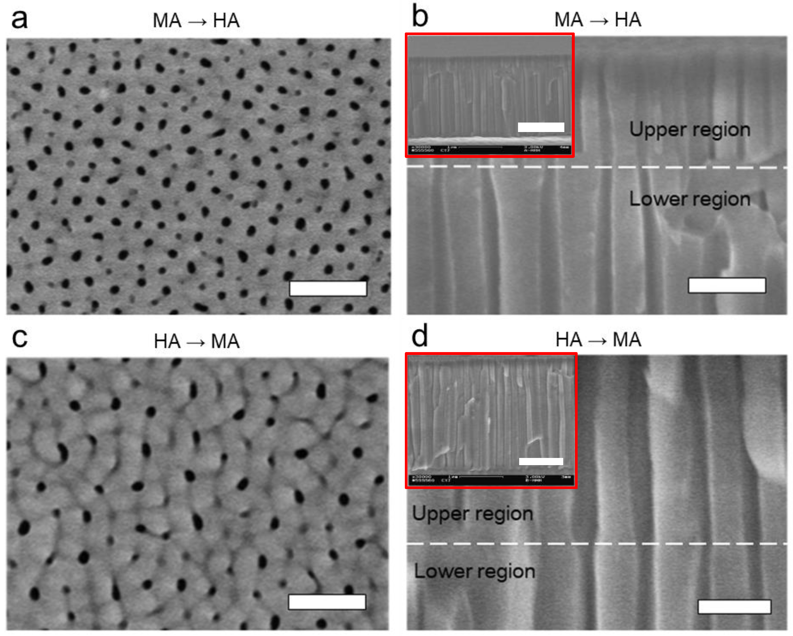
| - | MA | HA | Figure 3a,b | 24 ± 4.5 | 40 ± 6.9 | 81 ± 10.3 | 139 ± 13.8 | 0.087 ± 0.032 | 0.077 ± 0.025 |
| - | HA | MA | Figure 3c,d | 50 ± 14.7 | 38 ± 6.2 | 152 ± 10.1 | 154 ± 9.3 | 0.105 ± 0.049 | 0.058 ± 0.016 |
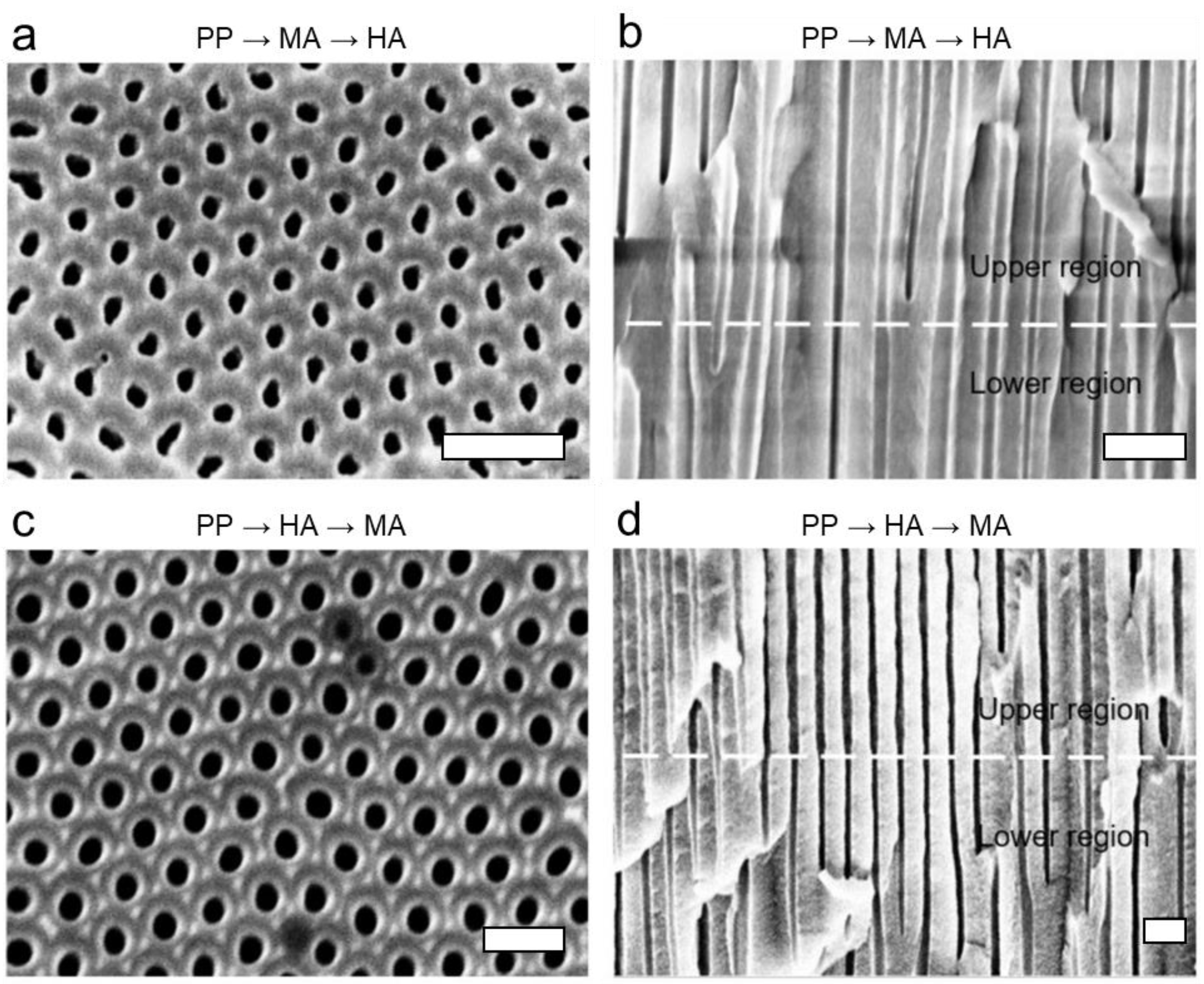
| PP | MA | HA | Figure 4a,b | 29 ± 1.7 | 41 ± 7.8 | 83 ± 7.6 | 150 ± 11.5 | 0.115 ± 0.020 | 0.070 ± 0.023 |
| PP | HA | MA | Figure 4c,d | 50 ± 3.3 | 41 ± 3.3 | 150 ± 4.2 | 150 ± 8.1 | 0.103 ± 0.012 | 0.069 ± 0.011 |
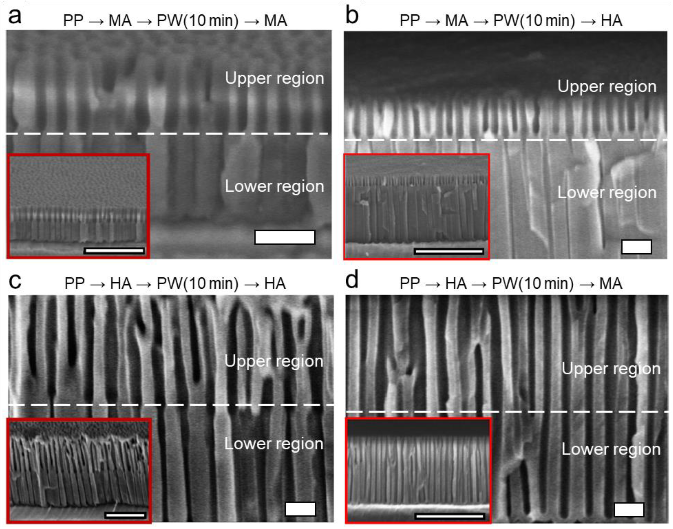
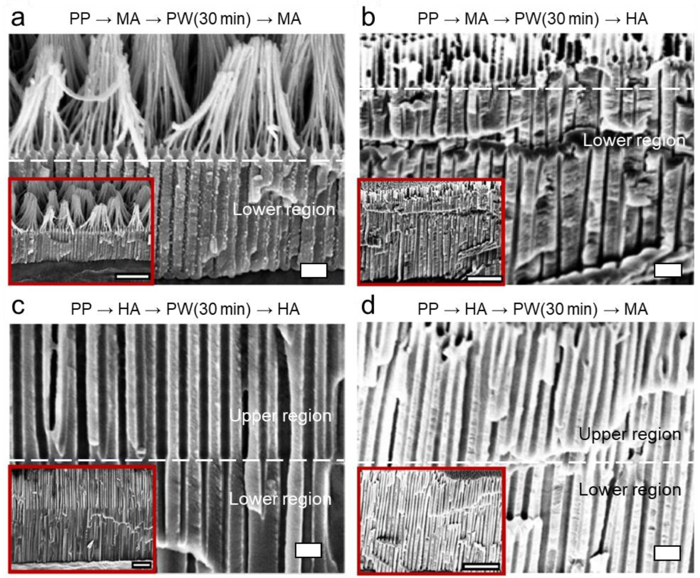
| 1st Anodizing Step (after PP) | PW Time (min) | 2nd Anodizing Step | Figures of Results | Pore Diameter, Dp (nm) | Interpore Distance, Dint (nm) | Porosity (ϕ) | Type in Figure 7 | |||||
|---|---|---|---|---|---|---|---|---|---|---|---|---|
| Type | Time (min) | Type | Time (min) | 1st Step with PW | 2nd Step | 1st Step with PW | 2nd Step | 1st Step with PW | 2nd Step | |||
| MA | 30 | 10 | MA | 30 | Figure 5a | 42 ± 3.8 | 20 ± 2.3 | 84 ± 12.6 | 85 ± 13.0 | 0.239 ± 0.069 | 0.051 ± 0.016 | a |
| MA | 30 | 30 | MA | 30 | Figure 6a | Pillared | 28 ± 3.8 | Pillared | 85 ± 3.7 | N/A | 0.102 ± 0.023 | b |
| MA | 30 | 0 | HA | 0.5 | Figure 4a,b | 29 ± 1.7 | 41 ± 7.8 | 83 ± 7.6 | 150 ± 11.5 | 0.115 ± 0.020 | 0.070 ± 0.023 | c |
| MA | 30 | 10 | HA | 0.5 | Figure 5b | 49 ± 2.5 | 40 ± 3.7 | 84 ± 12.9 | 149 ± 11.3 | 0.322 ± 0.086 | 0.068 ± 0.013 | d |
| MA | 30 | 30 | HA | 0.5 | Figure 6b | 60 ± 5.2 | 41 ± 3.1 | 84 ± 8.2 | 149 ± 12.0 | 0.390 ± 0.084 | 0.069 ± 0.013 | d |
| HA | 0.5 | 10 | HA | 0.5 | Figure 5c | 61 ± 7.3 | 42 ± 7.4 | 153 ± 9.3 | 153 ± 4.1 | 0.146 ± 0.032 | 0.069 ± 0.020 | a |
| HA | 0.5 | 30 | HA | 0.5 | Figure 6c | 65 ± 5.9 | 42 ± 5.4 | 155 ± 15.1 | 154 ± 15.0 | 0.164 ± 0.036 | 0.069 ± 0.018 | a |
| HA | 0.5 | 0 | MA | 30 | Figure 4c,d | 50 ± 3.3 | 41 ± 3.3 | 150 ± 4.2 | 150 ± 8.1 | 0.103 ± 0.012 | 0.069 ± 0.011 | a |
| HA | 0.5 | 10 | MA | 30 | Figure 5d | 61 ± 3.8 | 56 ± 4.2 | 151 ± 13.8 | 150 ± 11.0 | 0.151 ± 0.027 | 0.130 ± 0.022 | a |
| HA | 0.5 | 30 | MA | 30 | Figure 6d | 66 ± 9.8 | 65 ± 11.8 | 156 ± 13.5 | 156 ± 15.8 | 0.165 ± 0.046 | 0.268 ± 0143 | a |
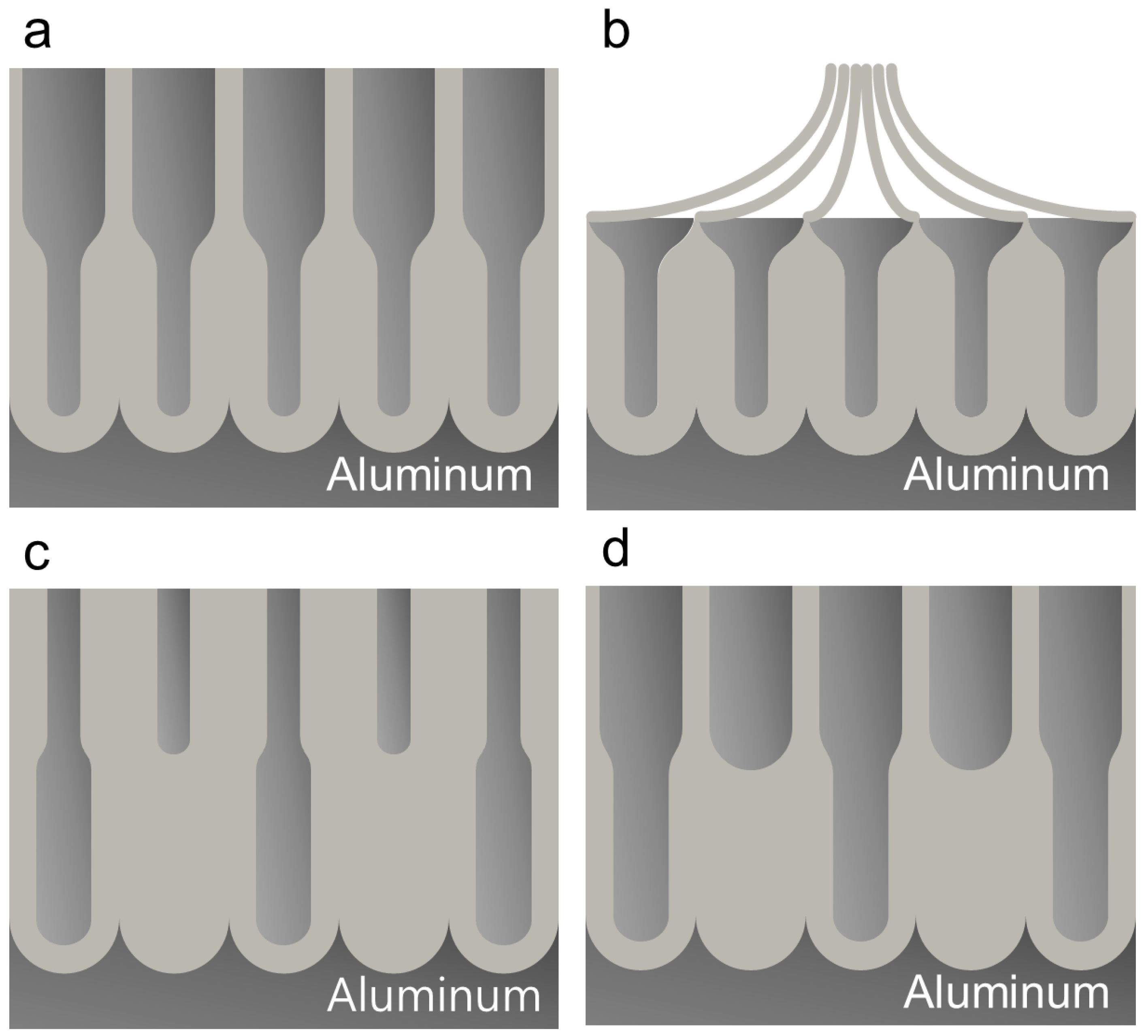
| Anodizing Step | Pore Shape | Pore Wall Merging at Transition | Schematic | Characteristics in Second Anodizing Step | |||
|---|---|---|---|---|---|---|---|
| First | Intermediate | Second | Dp | Dint | |||
| MA | PW | MA | Funnel to Pillar-on-pore | No merging | Figure 7a,b | Follows MA | Follows MA |
| MA | - | HA | Bottle | Y-shaped merging | Figure 7c | Follows HA | Follows HA |
| MA | PW | HA | Funnel | M-shaped merging | Figure 7d | Follows HA | Follows HA |
| HA | PW | HA | Funnel | No merging | Figure 7a | Follows HA | Follows HA |
| HA | - | MA | Funnel | No merging | Figure 7a | Follows MA | Follows HA |
| HA | PW | MA | Funnel | No merging | Figure 7a | Follows PW | Follows HA |
Disclaimer/Publisher’s Note: The statements, opinions and data contained in all publications are solely those of the individual author(s) and contributor(s) and not of MDPI and/or the editor(s). MDPI and/or the editor(s) disclaim responsibility for any injury to people or property resulting from any ideas, methods, instructions or products referred to in the content. |
© 2023 by the authors. Licensee MDPI, Basel, Switzerland. This article is an open access article distributed under the terms and conditions of the Creative Commons Attribution (CC BY) license (https://creativecommons.org/licenses/by/4.0/).
Share and Cite
Jeong, C.; Jung, J.; Sheppard, K.; Choi, C.-H. Control of the Nanopore Architecture of Anodic Alumina via Stepwise Anodization with Voltage Modulation and Pore Widening. Nanomaterials 2023, 13, 342. https://doi.org/10.3390/nano13020342
Jeong C, Jung J, Sheppard K, Choi C-H. Control of the Nanopore Architecture of Anodic Alumina via Stepwise Anodization with Voltage Modulation and Pore Widening. Nanomaterials. 2023; 13(2):342. https://doi.org/10.3390/nano13020342
Chicago/Turabian StyleJeong, Chanyoung, Jeki Jung, Keith Sheppard, and Chang-Hwan Choi. 2023. "Control of the Nanopore Architecture of Anodic Alumina via Stepwise Anodization with Voltage Modulation and Pore Widening" Nanomaterials 13, no. 2: 342. https://doi.org/10.3390/nano13020342