Article

Low-Temperature Solution-Processed HfZrO Gate Insulator for High-Performance of Flexible LaZnO Thin-Film Transistor

1
Advanced Display Research Center, Department of Information Display, Kyung Hee University, Seoul 02447, Republic of Korea
2
Department of Semiconductor Display, Gachon University, Seongnam-si 13120, Republic of Korea
3
School of Mechanical & Materials Engineering, Indian Institute of Technology Mandi, Mandi Pradesh 175075, India
*
Authors to whom correspondence should be addressed.
Nanomaterials 2023, 13(17), 2410; https://doi.org/10.3390/nano13172410
Submission received: 5 July 2023 / Revised: 1 August 2023 / Accepted: 16 August 2023 / Published: 25 August 2023
(This article belongs to the Topic Advances in Functional Thin Films)

Abstract

:
Metal-oxide-semiconductor (MOS)-based thin-film transistors (TFTs) are gaining significant attention in the field of flexible electronics due to their desirable electrical properties, such as high field-effect mobility (μFE), lower IOFF, and excellent stability under bias stress. TFTs have widespread applications, such as printed electronics, flexible displays, smart cards, image sensors, virtual reality (VR) and augmented reality (AR), and the Internet of Things (IoT) devices. In this study, we approach using a low-temperature solution-processed hafnium zirconium oxide (HfZrOx) gate insulator (GI) to improve the performance of lanthanum zinc oxide (LaZnO) TFTs. For the optimization of HfZrO GI, HfZrO films were annealed at 200, 250, and 300 °C. The optimized HfZrO-250 °C GI-based LaZnO TFT shows the μFE of 19.06 cm2V−1s−1, threshold voltage (VTH) of 1.98 V, hysteresis voltage (VH) of 0 V, subthreshold swing (SS) of 256 mV/dec, and ION/IOFF of ~108. The flexible LaZnO TFT with HfZrO-250 °C GI exhibits negligible ΔVTH of 0.25 V under positive-bias-temperature stress (PBTS). The flexible hysteresis-free LaZnO TFTs with HfZrO-250 °C can be widely used for flexible electronics. These enhancements were attributed to the smooth surface morphology and reduced defect density achieved with the HfZrO gate insulator. Therefore, the HfZrO/LaZnO approach holds great promise for next-generation MOS TFTs for flexible electronics.

1. Introduction

Metal oxide semiconductors (MOS) are gaining significant interest as channel layers in thin-film transistors (TFTs), particularly for active-matrix light-emitting diode (AMOLED) displays [1,2,3]. These materials exhibit desirable electrical properties, such as high mobility, near-zero threshold voltage, low off-state current, excellent area uniformity, reliability, and cost-effective mass production. MOS-based TFTs hold the potential to supplant conventional polycrystalline-Si (Poly-Si) or amorphous-Si (a-Si) TFTs across diverse applications. Their appeal lies in offering higher performance characteristics, including improved carrier mobility and lower off-state leakage. Moreover, MOS-based TFTs can be fabricated via cost-effective and scalable processes, making them a viable candidate for next-generation electronic devices. As a result, these TFTs present a compelling alternative for enhancing electronic technologies and fostering innovation in various industries [1,2,3]. The fabrication of MOS TFTs can be achieved through either solution [1,2,3,4,5] or vacuum process [1,6]. Solution processes [1,2,3,4,5], including spray pyrolysis, spin coating, and inkjet printing, are commonly employed for MOS TFT fabrication [7,8,9,10,11,12,13,14,15,16,17,18,19]. Solution processes offer the advantage of operating at low temperatures, facilitating the deposition of metal-oxide-semiconductor (MOS) films on flexible substrates. This characteristic is essential for the development of flexible electronics as it avoids substrate damage and allows for the fabrication of bendable and stretchable devices [1]. In solution-processed oxide TFTs, high-k dielectric materials, for example, aluminum oxide (AlOx) [12,20], hafnium oxide (HfOx) [21], zirconium oxide (ZrOx) [2,10,17,22], aluminum zirconium oxide (AlZrOx) [13,23], boron-doped ZrOx (BZrO) [9], hafnium zirconium oxide (HfZrOx) [24], and lanthanum-doped ZrOx (LaZrO), are employed to achieve high-performance devices. While other MO semiconductors, such as indium gallium tin oxide (IGTO) [25,26] and indium gallium zinc oxide (IGZO) [5] TFTs, typically utilize a SiO2 gate insulator, solution-processed oxide TFTs offer the advantage of utilizing high-k dielectrics for improved performance [8].
The utilization of high-k gate dielectric materials through solution processes holds tremendous promise in realizing high-performance thin-film transistors (TFTs). These materials offer advantageous electrical properties, such as higher dielectric constants, enabling enhanced control of charge carriers in the transistors. Additionally, the solution-based approach allows for cost-effective and scalable fabrication, making it a viable option for advancing next-generation electronic devices with improved efficiency and functionality. J. Li et al. report ZTO/AlZrOx TFT with μsat of 12.5 cm2V−1s−1, VTH of 0.3 V, ION/IOFF of 8 × 10⁷, and SS of 0.150 V/dec [27]. Tue et al. demonstrated the use of LaZrO gate dielectric in ZrInZnO TFTs, resulting in a saturated mobility (μsat) of 6.23 cm2V−1s−1, ION/IOFF of 109, and SS of 0.19 V/dec [8]. Park et al. report In2O3/ZrO2:B TFT with μsat of 39.3 cm2V−1s−1, VTH of 2.46 V, ION/IOFF of 107, and SS of 0.263 V/dec [9]. When considering practical applications, TFTs are fabricated on flexible plastic substrates, such as polyethylene naphthalate (PEN), polyethylene terephthalate (PET), and polyimide (PI). These plastic substrates offer mechanical flexibility, making them ideal candidates for foldable or flexible electronics and displays. Consequently, a low-temperature process becomes essential for compatibility with these substrates. Numerous research groups have focused on developing doped ZrOx gate insulators to enhance the performance of flexible metal oxide TFTs [2,22].
In this study, we present the utilization of a low-temperature solution-processed hafnium zirconium oxide (HfZrOx) GI to achieve high-performance LaZnO TFTs. The HfZrO films were carefully annealed at a temperature of 200, 250, and 300 °C, respectively, for optimization. The optimized HfZrO-250 °C GI-based LaZnO TFT demonstrates an impressive field-effect mobility (μFE) of 19.06 cm2V−1s−1, a low threshold voltage (VTH) of 1.98 V, and an exceptionally sharp subthreshold swing (SS) of 256 mV/dec. Notably, the device exhibits zero hysteresis voltage (VH) and an outstanding ION/IOFF ratio of ~108, ensuring high-performance transistor operation. Furthermore, the flexible HfZrO-250 °C/LaZnO TFT exhibits remarkable stability under positive-bias-temperature stress (PBTS) with minimal ΔVTH, indicating the reliability of the device over the extended operation. These exceptional enhancements can be attributed to the smooth surface morphology achieved by the HfZrO GI and the reduced defects at the interface between the HfZrO gate insulator and the oxide semiconductor (LaZnO). Our findings establish the HfZrO/LaZnO approach as a highly promising avenue for developing flexible oxide TFTs, especially for next-generation flexible displays. The novel combination of materials and the low-temperature solution processing offer significant potential for advancing flexible electronics.

2. Materials and Methods

To prepare the HfZrO precursor solution, we dissolved zirconyl chloride hydrated (ZrOCl·8H2O) and hafnium chloride (HfCl4) in a mixture of ethylene glycol (65%) and acetonitrile (35%). The resulting solution, 20 mL in volume, was transferred to a 0.250 L flask. The temperature was steadily increased from room temperature (RT) to 95 °C in 10 °C increments. The solution was maintained at 95 °C for 10 min, resulting in the formation of a transparent precursor solution after cooling to RT. For the synthesis of the 0.2 M LaZnO precursor solution, zinc acetate dihydrate, lanthanum (III) nitrate hexahydrate, and ammonium acetate were added to a solvent called 2-Methoxyenthonal (2ME). The stoichiometry of HZO and LaZnO films are H0.10Z0.90O and La0.10Zn0.90O, respectively. The detailed method for preparing the HZO and LaZnO precursor solution can be found elsewhere [2,24]. The precursor solutions were stirred for 2 h under an N2 environment to ensure homogeneity. Finally, a 0.45 µm polytetrafluoroethylene (PTFE) filter was employed to obtain particle-free precursor solutions.
The HfZrO film was deposited via spin coating onto a glass substrate at room temperature in the ambient environment. After deposition, the sample was placed on a hot plate at 140 °C for 5 min and subsequently annealed in an air furnace at temperatures ranging from 200 to 300 °C. The resulting HfZrO thin films were labeled as HfZrO-200 °C, HfZrO-250 °C, and HfZrO-300 °C, corresponding to the annealing temperatures. The LaZnO film, on the other hand, was deposited using spray pyrolysis onto a glass substrate at a substrate temperature of 350 °C.
In our fabrication process, we employed a bottom gate and top contact configuration for the LaZnO TFTs. Initially, a 40 nm molybdenum (Mo) film was sputtered onto the substrate and patterned to create the gate electrodes. Following the deposition of the HfZrO film, the sample was subjected to a 5 min treatment on a hotplate at 140 °C. The LaZnO solution was then deposited onto the substrate at a temperature of 350 °C using spray pyrolysis. The thickness of the LaZnO films was measured using the Alpha-Step D-500 Stylus Profiler (D-500 Stylus Profiler, KLA Instrument, Hayward, CA, USA). The LaZnO layer was patterned using conventional photolithography to form the active island. Finally, a 40 nm thick Mo layer was sputtered and patterned to create the source/drain (S/D) electrodes.
For the fabrication of flexible LaZnO TFTs, we employed a bottom gate and top contact (BGTC) structure on a polyimide (PI) substrate. Initially, a thin layer of carbon nanotube‒graphene oxide (CNT:GO) composite was deposited through spray pyrolysis at 100 °C [3,8]. Subsequently, a 10 μm thick PI layer was spin-coated onto the CNT:GO layer and annealed for 2 h under a nitrogen (N2) atmosphere. To provide a gas barrier, a SiNx/SiOx buffer layer with a total thickness of 125 nm (25 nm for each layer) was deposited. The LaZnO channel layer was then deposited at a substrate temperature of 350 °C via spray pyrolysis. The LaZnO active islands were patterned. Finally, a 40 nm molybdenum (Mo) layer was sputtered and patterned to create the source/drain (S/D) contacts. For a detailed fabrication process flow of the LaZnO TFT, refer to the appropriate literature [2,17].
To characterize the HfZrOx films, we conducted UV-visible spectroscopy (transmittance and absorbance) using a Scinco S-4100 instrument. The film thickness was measured with an Alpha step, while the refractive index was determined using ellipsometry. Surface morphology (including RMS roughness) was examined using atomic force microscopy (AFM). Chemical composition and elemental analysis of the metal oxide films were studied through X-ray photoelectron spectroscopy (XPS) with a PHI 5000 Versa Probe (PHI 5000 Versa Probe, Ulvac-PHI, Chigasaki, Japan) under pressure of 7.5 × 10⁻⁵ mTorr.
The electrical properties of TFTs were measured using an Agilent 4156C semiconductor parameter analyzer. The measurements were conducted at room temperature under dark conditions. The VTH was determined by employing the linear extrapolation method on the (IDS)1/2 vs. VGS plot, using the x-axis intercept. The μsat was obtained from the linear section of the (IDS)1/2 vs. VGS curve. The SS was determined from the linear region of the log (IDS) vs. VGS fit using Formula (2).
I D S = 1 2 W L μ s a t C o x ( V G S V T H ) 2 ,
S S = d V G S d ( l o g   I   D S )
where IDS, W/L, μsat, Cox, VTH, and VGS are the drain current, channel width, channel length, saturation mobility, gate oxide capacitance, threshold voltage, and gate voltage, respectively.

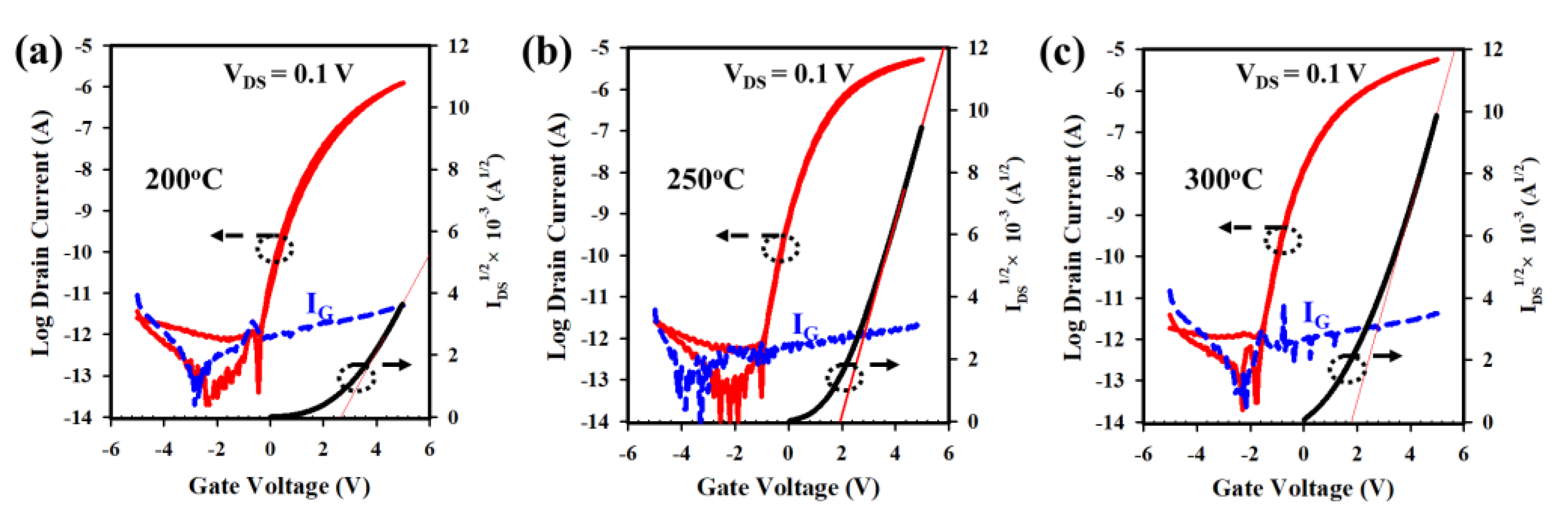
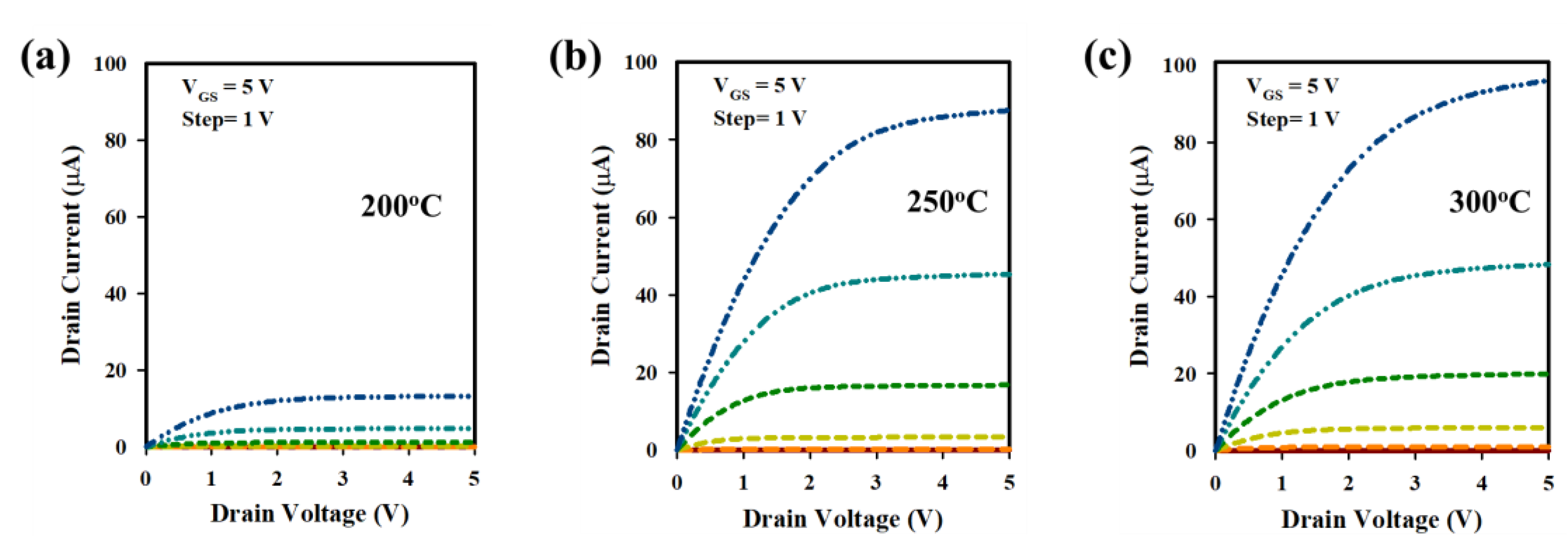
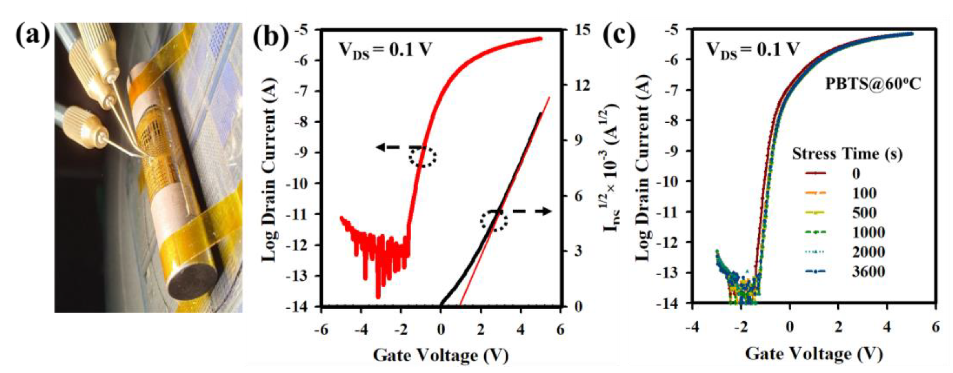
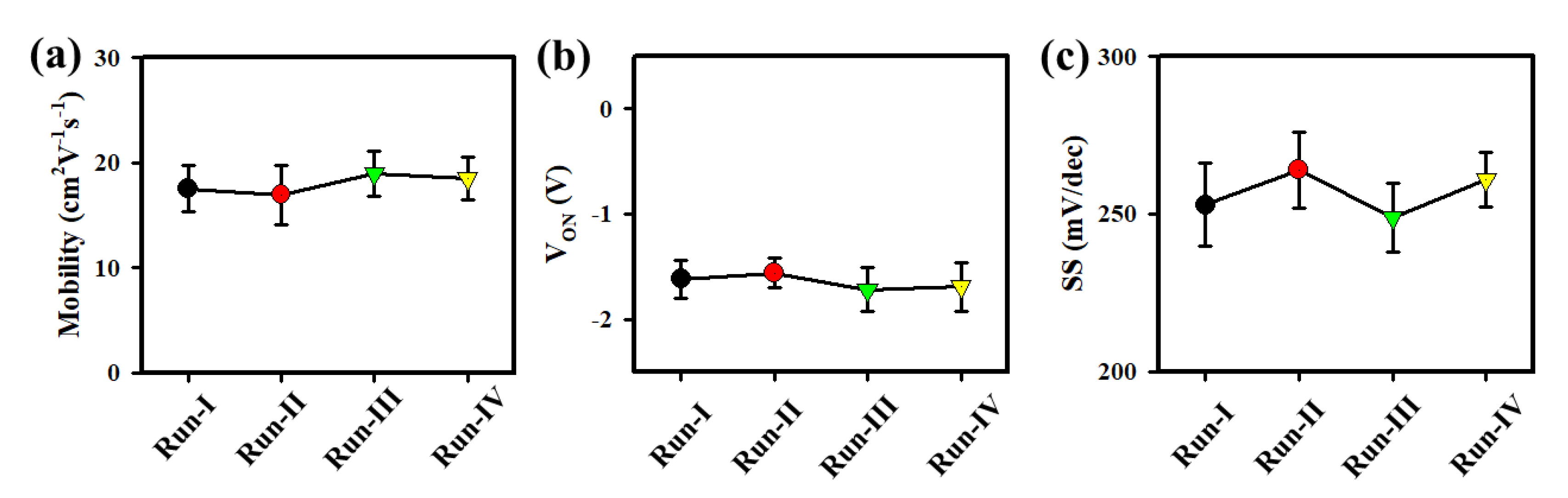
3. Results and Discussion

Figure 1a illustrates the process flow for fabricating the HfZrOx thin film on a glass substrate. Further details can be found in the Materials and Methods Section. In Figure 1b, it is evident that the HfZrOx thin film exhibits transmittances exceeding 90% in the visible region. The optical band gaps of HfZrO-200 °C, HfZrO-250 °C, and HfZrO-300 °C thin films are shown in Figure 1c. For the UV-Vis experiment, the HfZrOx films were deposited on the glass, where the absorption of a glass substrate can be negligible [2]. The band gap (Eg) of HfZrO-250 °C is 5.85 eV, as can be seen in Figure 1c [2,28,29,30,31]. The Eg was extracted using the formula: αhν = A (hν − Eg)1/n, where hν, n, A, and α are the photon energy, optical transition exponent, a proportionality constant in the absorption process, and absorption coefficient, respectively. The refractive index (R.I.) of HfZrOx films was measured by ellipsometry. Figure 1d displays the refractive indices (RI) of HfZrO-200 °C, HfZrO-250 °C, and HfZrO-300 °C, with corresponding values of 1.68, 1.79, and 1.83, respectively. The increase in film density is evident from the RI values observed in the visible range. In metal oxide thin film, the composition of the film density can be correlated with RI values. As the annealing temperature increases, the film density of HfZrOx also increases. A lower RI value indicates an increase in film porosity, which subsequently affects both the optical and electrical properties [2,17,28,29,30].
Figure 2 illustrates the frequency-dependent capacitance of the HfZrO-200 °C, HfZrO-250 °C, and HfZrO-300 °C GIs. The capacitance was measured with a frequency from 20 Hz to 2 MHz. The capacitance values of HfZrO-200 °C, HfZrO-250 °C, and HfZrO-300 °C are 384, 455, and 476 nF/cm2, respectively. In the capacitance curve of the HfZrOx film annealed at 200 °C, a decrease in capacitance is observed from around 10 kHz, while the capacitance remains constant up to 300 kHz for HfZrOx-300 °C, with degradation commencing at 300 kHz. This behavior is attributed to the lower defect density present in the HfZrOx film annealed at 200 °C [24]. The inset in Figure 2 depicts the MIM (Mo/HfZrOx/Mo) structure.
Figure 3a–c presents the surface morphology of HfZrO-200 °C, HfZrO-250 °C, and HfZrO-300 °C films. The root-mean-square roughness (RRMS) values for the HfZrOx films annealed at 200 °C, 250 °C, and 300 °C are determined to be 0.57 nm, 0.36 nm, and 0.29 nm, respectively, with a scanning area of 2 μm × 2 μm. With increasing annealing temperature, the surface roughness decreases, resulting in a smoother surface morphology [20]. The improved smoothness of the HfZrOx film surface enhances the interface quality with the channel layer. Consequently, the favorable interface between the gate insulator and the channel layer contributes to the enhanced electrical properties of the LaZnO TFT [2,8,12,20,24,25,26,29,30].
The O1s XPS spectra were analyzed to investigate the chemical composition of the HfZrO films (Figure 4a–c). The O 1s peak was deconvoluted into three sub-peaks centered around ~529.5 eV (metal oxide, M-O), ~530.5 eV (oxygen vacancy, Vo), and ~532 eV (hydroxyl groups, -OH). The percentages of M-O-M, Vo, and -OH in the HfZrOx films annealed at different temperatures (200 °C, 250 °C, and 300 °C) were determined. The M-O-M percentages were found to be 64.75%, 75.39%, and 77.65%, while the Vo ratios were 24.75%, 17.28%, and 15.98%, and the -OH ratios were 10.50%, 7.33%, and 6.37%, respectively [2,15]. The higher M-O-M content indicates a reduction in oxygen-related defects (Vo + -OH), resulting in fewer defects at the interface between the gate insulator and channel layers. This contributes to improved device performance and interface quality [5,10,14,15,27,31,32,33].
The electrical properties of LaZnO TFTs with HfZrO (HfZrO-200 °C, HfZrO-250 °C, and HfZrO-300 °C) gate insulators were studied by measuring the I-V (transfer) curves of TFTs. Figure 5a–c depicts the transfer curves of LaZnO TFTs with HfZrO-200 °C, HfZrO-250 °C, and HfZrO-300 °C, illustrating their hysteresis characteristics, with corresponding electrical properties, such as μFE of (8.49, 19.06, and 22.28) cm2V−1s−1, VTH of (2.60, 1.98, and 1.87) V, VH of (0.03, 0, and 0) V, and SS of (295, 256, and 231) mV/dec, respectively. The hysteresis curves for the LaZnO TFTs with HfZrO-200 °C, HfZrO-250 °C, and HfZrO-300 °C show the negligible VH, indicating a favorable gate insulator (GI)/channel interface. The reduced number of traps at the GI/channel interface contributes to higher ION and lower SS, as shown in Figure 5a–c. Achieving a higher M-O-M ratio and minimizing oxygen-related defects leads to smoother charge transport and reduced charge trapping, resulting in enhanced carrier mobility and stable device operation. With an increase in HfZrOx annealing temperature, the VTH shifts to a positive VGS due to a decrease in trap states at the interface [2,10,24,33]. The output curves of LaZnO TFTs with HfZrO-200 °C, HfZrO-250 °C, and HfZrO-300 °C are presented in Figure 6a–c, exhibiting clear pinch-off and saturation behavior. The TFTs were tested with VDS sweeping from 0 to +5 V and VGS sweeping from 0 to +5 V (step = 1 V). The absence of current crowding in the low VDS region confirms excellent ohmic contact between the source/drain electrodes and channel layers [5,10,16,29].
Figure 7a presents an optical photograph of the measurement setup for the flexible LaZnO TFT fabricated on a PI substrate with a HfZrO-250 °C gate insulator (GI). Figure 7b displays the transfer curve of the flexible LaZnO TFT, measured at VDS of 0.1 V by sweeping VGS from −5 to +5 V. The IDS1/2 vs. VGS plot with a linear extrapolation line is shown on the right side of the y-axis. The flexible LaZnO TFT with HfZrO-250 °C GI exhibits a μFE of 20.55 cm2V−1s−1, VTH of 1.12 V, and SS of 264 mV/dec. Compared with TFTs on glass substrates, the electrical properties of the flexible LaZnO TFT show almost negligible changes. To assess the bias stability of the LaZnO TFT with HfZrO-250 °C GI, PBTS was performed on the TFT (at VGS = 5 V for 1 h), as shown in Figure 7c. The evaluation of the transfer curve under PBTS reveals a threshold voltage shift (ΔVTH) of 0.25 V. The positive shift in VTH is attributed to electron trapping at the interface between the HfZrO and LaZnO layers. However, the SS of the LaZnO TFT undergoes a negligible change after 1 h of bias stress, indicating fewer interfacial traps. A higher M-O-M ratio and reduced oxygen-related defects significantly enhance mobility and excellent bias stability of the metal oxide TFT. Thus, the interface quality between HfZrOx and LaZnO plays a crucial role in improving the electrical properties of the TFT.
To validate the accuracy of the performances of HfZrO-250 °C/LaZnO TFTs, we fabricated the TFTs in four different runs to ensure precise and reliable data collection. The mFE, VON, and SS values of the HfZrO-250 °C/LaZnO TFT for Run-I, Run-II, Run-III, and Run-IV are (17.50 ± 2.20, 16.95 ± 2.85, 18.99 ± 2.15, and 18.50 ± 1.98) cm2V−1s−1, (−1.62 ± 0.18, −1.56 ± 0.14, −1.72 ± 0.21, and −1.69 ± 0.23) V, (253 ± 13.22, 264 ± 11.94, 249 ± 10.89, and 261 ± 8.58) mV/dec, respectively, as shown in Figure 8a–c. The small deviation in these values indicates the high reliability and consistency of the fabrication process. The narrow range of fluctuations highlights the robustness of the HfZrO-250 °C/LaZnO TFT performance across multiple runs, reaffirming its potential for practical applications in electronic devices. The HZO film deposited at 350 °C is prone to crystallization and can be a ferroelectric material [33]. As a result, we used spin-coating for the HZO film at 250 °C, which provides a more favorable gate insulator for the LaZnO TFT. The electrical properties of the solution-processed ZnO-based TFTs with various solution-processed gate dielectrics are reported in the literature, as shown in Table 1 [34,35,36,37,38,39]. H. Liu et al., demonstrate hysteresis-free Indium gallium zinc oxide (IGZO) TFT with HfOx gate insulator (GI), which exhibits excellent performance characteristics, including a high mobility of 30 cm2V−1s−1, an SS of 68 mV/dec, and a high ION/IOFF of 106 [40]. In the present work, our HfZrO/LaZnO TFTs display superior performance with high mobility, low subthreshold swing, and a high ION/IOFF ratio. Furthermore, we successfully fabricated flexible LaZnO TFTs with HfZrO-250 °C GI, which exhibited hysteresis-free behavior, leading to improved electronic device performance and enhanced stability for a wide range of applications [34,35,36,41].

4. Conclusions

In summary, this study investigates the use of a low-temperature solution-processed HfZrOx gate insulator (GI) to improve the performance of LaZnO thin-film transistors (TFTs) for potential applications in next-generation flexible displays. To optimize the HfZrO GI, annealing was performed at 200, 250, or 300 °C. The LaZnO TFT with HfZrO-250 °C GI exhibits a μFE of 19.06 cm2V−1s−1, VTH of 1.98 V, hysteresis voltage (VH) of 0 V, SS of 256 mV/dec, and ION/IOFF ratio of ~108. The decrease in hysteresis voltage is critical as it helps to ensure the stability and reliability of the TFT operation. Additionally, the steep subthreshold slope (SS) of 256 mV/dec indicates a sharp turn-on behavior, which is essential for achieving efficient switching. Moreover, the on/off current ratio (ION/IOFF) of ~108 highlights the ability of the transistor to efficiently control the flow of currents. Under PBTS, the HfZrO-250 °C/LaZnO TFT experiences a threshold voltage shift (ΔVTH) of 0.23 V. These enhancements can be attributed to the smooth surface morphology and reduced defects in the HfZrO gate insulator. Therefore, these findings significantly advance our understanding of the underlying phenomena and pave the way for the development of flexible metal-oxide-semiconductor TFTs for future-generation flexible displays.

Author Contributions

Conceptualization, R.N.B.; Y.C. and J.J.; methodology, Y.C. and R.N.B.; formal analysis, R.N.B. and Y.C.; investigation, R.N.B. and Y.C.; resources, R.N.B. and J.J.; data curation, Y.C.; J.B.; R.N.B. and J.J.; writing—original draft preparation, R.N.B. and Y.C.; writing—review and editing, R.N.B. and J.J.; supervision, J.J.; funding acquisition, J.J. All authors have read and agreed to the published version of the manuscript.

Funding

This work was supported by the Industrial Strategic Technology Development Program (20010082) funded by the MOTIE, Korea.

Data Availability Statement

We can provide the data if asked.

Conflicts of Interest

The authors declare no conflict of interest.

References

  1. Zhang, L.; Li, J.; Zhang, X.W.; Jiang, X.Y.; Zhang, Z.L. High Performance ZnO-Thin-Film Transistor with Ta2O5 Dielectrics Fabricated at Room Temperature. Appl. Phys. Lett. 2009, 95, 23–26. [Google Scholar] [CrossRef]
  2. Bukke, R.N.; Saha, J.K.; Mude, N.N.; Kim, Y.; Lee, S.; Jang, J. Lanthanum Doping in Zinc Oxide for Highly Reliable Thin-Film Transistors on Flexible Substrates by Spray Pyrolysis. ACS Appl. Mater. Interfaces 2020, 12, 35164–35174. [Google Scholar] [CrossRef] [PubMed]
  3. Chen, R.; Lan, L. Solution-Processed Metal-Oxide Thin-Film Transistors: A Review of Recent Developments. Nanotechnology 2019, 30, 312001. [Google Scholar] [CrossRef]
  4. Jeong, H.J.; Ok, K.C.; Park, J.; Lim, J.; Cho, J.; Park, J.S. Stability Improvement of In-Sn-Ga-O Thin-Film Transistors at Low Annealing Temperatures. IEEE Electron Device Lett. 2015, 36, 1160–1162. [Google Scholar] [CrossRef]
  5. Park, W.; Park, J.-H.; Eun, J.-S.; Lee, J.; Na, J.-H.; Lee, S.-H.; Jang, J.; Kang, I.M.; Kim, D.-K.; Bae, J.-H. Low-Temperature Enhancement-Mode Amorphous Oxide Thin-Film Transistors in Solution Process Using a Low-Pressure Annealing. Nanomaterials 2023, 13, 2231. [Google Scholar] [CrossRef]
  6. Shin, S.W.; Cho, J.E.; Lee, H.M.; Park, J.S.; Kang, S.J. Photoresponses of InSnGaO and InGaZnO Thin-Film Transistors. RSC Adv. 2016, 6, 83529–83533. [Google Scholar] [CrossRef]
  7. Faber, H.; Butz, B.; Dieker, C.; Spiecker, E.; Halik, M. Fully Patterned Low-Voltage Transparent Metal Oxide Transistors Deposited Solely by Chemical Spray Pyrolysis. Adv. Funct. Mater. 2013, 23, 2828–2834. [Google Scholar] [CrossRef]
  8. Tue, P.T.; Miyasako, T.; Li, J.; Tu, H.T.C.; Inoue, S.; Tokumitsu, E.; Shimoda, T. High-performance solution-processed ZrInZnO thin-film transistors. IEEE Trans. Electron Devices 2013, 60, 320–326. [Google Scholar] [CrossRef]
  9. Park, J.H.; Yoo, Y.B.; Lee, K.H.; Jang, W.S.; Oh, J.Y.; Chae, S.S.; Lee, H.W.; Han, S.W.; Baik, H.K. Boron doped peroxo-zirconium oxide dielectric for high-performance, low-temperature, solution-processed indium oxide thin-film transistor. ACS Appl. Mater. Interfaces 2013, 5, 8067–8075. [Google Scholar] [CrossRef]
  10. Bukke, R.N.; Avis, C.; Naik, M.N.; Jang, J. Remarkable Increase in Field Effect Mobility of Amorphous IZTO Thin-Film Transistors with Purified ZrOx Gate Insulator. IEEE Electron Device Lett. 2018, 39, 371–374. [Google Scholar] [CrossRef]
  11. Wang, D.; Jiang, Z.; Li, L.; Zhu, D.; Wang, C.; Han, S.; Fang, M.; Liu, X.; Liu, W.; Cao, P.; et al. High-Performance Thin-Film Transistors with ZnO:H/ZnO Double Active Layers Fabricated at Room Temperature. Nanomaterials 2023, 13, 1422. [Google Scholar] [CrossRef] [PubMed]
  12. Han, Y.-J.; Lee, S.H.; Bak, S.-Y.; Han, T.-H.; Kim, S.; Yi, M. Performance Improvement of ZnSnO Thin-Film Transistors with Low-Temperature Self-Combustion Reaction. Electronics 2021, 10, 1099. [Google Scholar] [CrossRef]
  13. Liu, G.; Liu, A.O.; Zhu, H.; Shin, B.; Fortunato, E.; Martins, R.; Wang, Y.; Shan, F. Low-Temperature, Nontoxic Water-Induced Metal-Oxide Thin Films and Their Application in Thin-Film Transistors. Adv. Funct. Mater. 2015, 25, 2564–2572. [Google Scholar] [CrossRef]
  14. Yeom, H.I.; Ko, J.B.; Mun, G.; Park, S.H.K. High Mobility Polycrystalline Indium Oxide Thin-Film Transistors by Means of Plasma-Enhanced Atomic Layer Deposition. J. Mater. Chem. C 2016, 4, 6873–6880. [Google Scholar] [CrossRef]
  15. Li, J.; Huang, C.X.; Fu, Y.Z.; Zhang, J.H.; Jiang, X.; Zhang, Y. Amorphous LaZnSnO Thin Films by a Combustion Solution Process and Application in Thin Film Transistors. Electron. Mater. Lett. 2016, 12, 76–81. [Google Scholar] [CrossRef]
  16. Parthiban, S.; Kwon, J.Y. Role of Dopants as a Carrier Suppressor and Strong Oxygen Binder in Amorphous Indium-Oxide-Based Field Effect Transistor. J. Mater. Res. 2014, 29, 1585–1596. [Google Scholar] [CrossRef]
  17. Bukke, R.N.; Naik Mude, N.; Mobaidul Islam, M.; Jang, J. Improvement of Metal-Oxide Films by Post Atmospheric Ar/O2 Plasma Treatment for Thin Film Transistors with High Mobility and Excellent Stability. Appl. Surf. Sci. 2021, 568, 150947. [Google Scholar] [CrossRef]
  18. Kim, H.A.; Kim, J.O.; Hur, J.S.; Son, K.S.; Lim, J.H.; Cho, J.; Jeong, J.K. Achieving High Mobility in IGTO Thin-Film Transistors at a Low Temperature via Film Densification. IEEE Trans. Electron Devices 2018, 65, 4854–4860. [Google Scholar] [CrossRef]
  19. Hur, J.S.; Kim, J.O.; Kim, H.A.; Jeong, J.K. Stretchable Polymer Gate Dielectric by Ultraviolet-Assisted Hafnium Oxide Doping at Low Temperature for High Performance Indium Gallium Tin Oxide Transistors. ACS Appl. Mater. Interfaces 2019, 11, 21675–21685. [Google Scholar] [CrossRef]
  20. Wu, Y.; Lan, L.; He, P.; Lin, Y.; Deng, C.; Chen, S.; Peng, J. Influence of Hydrogen Ions on the Performance of Thin-Film Transistors with Solution-Processed AlOx Gate Dielectrics. Appl. Sci. 2021, 11, 4393. [Google Scholar] [CrossRef]
  21. Kim, D.H.; Cha, H.S.; Jeong, H.S.; Hwang, S.H.; Kwon, H.I. Effects of Active Layer Thickness on the Electrical Characteristics and Stability of High-Mobility Amorphous Indium–Gallium–Tin Oxide Thin-Film Transistors. Electronics 2021, 10, 1295. [Google Scholar] [CrossRef]
  22. Bukke, R.N.; Jang, J. Gel-Based Precursors for the High-Performance of n-Channel GaInSnZnO and p-Channel CuGaSnSO Thin-Film Transistors. RSC Adv. 2021, 11, 34392–34401. [Google Scholar] [CrossRef] [PubMed]
  23. Zhu, L.; He, G.; Zhang, C.; Yang, B.; Xia, Y.; Alam, F.; Zhang, Y. Water-Derived All-Oxide Thin-Film Transistors with ZrAlOx Gate Dielectrics and Exploration in Digital Circuits. IEEE Trans. Electron Devices 2019, 66, 4198–4204. [Google Scholar] [CrossRef]
  24. Bukke, R.N.; Mude, N.N.; Lee, J.; Avis, C.; Jang, J. Effect of Hf Alloy in ZrOx Gate Insulator for Solution Processed a-IZTO Thin Film Transistors. IEEE Electron Device Lett. 2019, 40, 32–35. [Google Scholar] [CrossRef]
  25. Kim, H.; Maeng, S.; Lee, S.; Kim, J. Improved Performance and Operational Stability of Solution-Processed InGaSnO (IGTO) Thin Film Transistors by the Formation of Sn-O Complexes. ACS Appl. Electron. Mater. 2021, 3, 1199–1210. [Google Scholar] [CrossRef]
  26. Chen, S.; Li, Y.; Lin, Y.; He, P.; Long, T.; Deng, C.; Chen, Z.; Chen, G.; Tao, H.; Lan, L.; et al. Inkjet-Printed Top-Gate Thin-Film Transistors Based on InGaSnO Semiconductor Layer with Improved Etching Resistance. Coatings 2020, 10, 425. [Google Scholar] [CrossRef]
  27. Li, J.; Huang, C.X.; Zhao, C.Y.; Zhong, D.Y.; Zhang, J.H.; Li, X.F. Feasibility of Atomic Layer Deposited AlZrOx Film to Achieve High Performance and Good Stability of ZnSnO-TFT. IEEE Trans. Electron Devices 2017, 64, 4959–4964. [Google Scholar] [CrossRef]
  28. Girtan, M.; Hrostea, L.; Boclinca, M.; Negulescu, B. Study of Oxide/Metal/Oxide Thin Films for Transparent Electronics and Solar Cells Applications by Spectroscopic Ellipsometry. AIMS Mater. Sci. 2017, 4, 594–613. [Google Scholar] [CrossRef]
  29. He, F.; Qin, Y.; Wan, L.; Su, J.; Lin, Z.; Zhang, J.; Chang, J.; Wu, J.; Hao, Y. Metal-oxide heterojunctions for high performance solution grown oxide thin film transistors. Appl. Surf. Sci. 2020, 527, 146774–146781. [Google Scholar] [CrossRef]
  30. Bukke, R.N.; Mude, N.N.; Bae, J.; Jang, J. Nano-Scale Ga-O Interface Engineering for High-Performance of ZnO-Based Thin-Film Transistors. ACS Appl. Mater. Interfaces 2022, 14, 41508–41519. [Google Scholar] [CrossRef]
  31. Carlos, E.; Martins, R.; Fortunato, E.; Branquinho, R. Solution Combustion Synthesis: Towards a Sustainable Approach for Metal Oxides. Chem. Eur. J. 2020, 26, 9099–9125. [Google Scholar] [CrossRef] [PubMed]
  32. Fan, W.-T.; Liu, P.-T.; Kuo, P.-Y.; Chang, C.-M.; Liu, I.-H.; Kuo, Y. Numerical Analysis of Oxygen-Related Defects in Amorphous In-W-O Nanosheet Thin-Film Transistor. Nanomaterials 2021, 11, 3070. [Google Scholar] [CrossRef] [PubMed]
  33. Park, J.W.; Kang, B.H.; Kim, H.J. A Review of Low-Temperature Solution-Processed Metal Oxide Thin-Film Transistors for Flexible Electronics. Adv. Funct. Mater. 2019, 21, 1904632–1904671. [Google Scholar]
  34. Singh, A.K.; Kharche, V.V.; Chakrabarti, P. Performance Optimization of ZnO based Thin Film Transistor for Future Generation Display Technology. In Proceedings of the 2017 14th IEEE India Council International Conference (INDICON), Roorkee, India, 15–17 December 2017; pp. 1–5. [Google Scholar]
  35. Afouxenidis, D.; Mazzocco, R.; Vourlias, G.; Livesley, P.J.; Krier, A.; Milne, W.I.; Kolosov, O.; Adamopoulos, G. ZnO-Based Thin Film Transistors Employing Aluminum Titanate Gate Dielectrics Deposited by Spray Pyrolysis at Ambient Air. ACS Appl. Mater. Interfaces 2015, 7, 7334–7341. [Google Scholar] [CrossRef]
  36. Esro, M.; Vourlias, G.; Somerton, C.; Milne, W.I.; Adamopoulos, G. High-Mobility ZnO Thin Film Transistors Based on Solution-processed Hafnium Oxide Gate Dielectrics. Adv. Funct. Mater. 2015, 25, 134–141. [Google Scholar] [CrossRef]
  37. Ding, X.; Yang, B.; Xu, H.; Qi, J.; Li, X.; Zhang, J. Low-Temperature Fabrication of IZO Thin Film for Flexible Transistors. Nanomaterials 2021, 11, 2552. [Google Scholar] [CrossRef]
  38. Jeong, Y.; Pearson, C.; Kim, H.G.; Park, M.Y.; Kim, H.; Do, L.M.; Petty, M.C. Optimization of a Solution-Processed SiO2 Gate Insulator by Plasma Treatment for Zinc Oxide Thin Film Transistors. ACS Appl. Mater. Interfaces 2016, 8, 2061–2070. [Google Scholar] [CrossRef]
  39. Xu, H.; Ding, X.; Qi, J.; Yang, X.; Zhang, J. A Study on Solution-Processed Y2O3 Films Modified by Atomic Layer Deposition Al2O3 as Dielectrics in ZnO Thin Film Transistor. Coatings 2021, 11, 969. [Google Scholar] [CrossRef]
  40. Liu, H.; Jing, L.; He, K.; Qu, D.; Li, Y.; Minari, T.; Tao, R.; Lu, X.; Liu, J. High Performance and Hysteresis-Free a-IGZO Thin Film Transistors Based on Spin-coated Hafnium Oxide Gate Dielectrics. IEEE Electron Device Lett. 2023, 1. [Google Scholar] [CrossRef]
  41. Kim, Y.G.; Lv, D.; Huang, J.; Bukke, R.N.; Chen, H.; Jang, J. Artificial Indium-Tin-Oxide Synaptic Transistor by Inkjet Printing Using Solution-Processed ZrOx Gate Dielectric. Phys. Status Solidi A 2020, 217, 2000314–2000321. [Google Scholar] [CrossRef]
Figure 1. (a) Schematic representation of HfZrOx thin film deposited by spin coating. (b) The transmittances of HfZrO-200 °C, HfZrO-250 °C, and HfZrO-300 °C thin films are higher than 90% in the visible region. (c) The bandgap of HfZrO-250 °C thin film obtained from the Tauc plot. The inset of (c) shows a photograph of HfZrO-250 °C thin film placed on the ADRC logo. (d) The refractive index as a function of the photon energy of HfZrO-200 °C, HfZrO-250 °C, and HfZrO-300 °C thin films.
Nanomaterials 13 02410 g001
Figure 2. Capacitance vs. frequency of HfZrO-200 °C, HfZrO-250 °C, and HfZrO-300 °C gate insulators (GIs) annealed at different temperatures.
Nanomaterials 13 02410 g002
Figure 3. AFM images (Scan size 2 μm × 2 μm) of (a) HfZrO-200 °C, (b) HfZrO-250 °C, and (c) HfZrO-300 °C thin films. The RRMS values of 0.57, 0.36, and 0.29 nm indicate smooth surface morphology.
Nanomaterials 13 02410 g003
Figure 4. Deconvoluted O1s spectra of (a) HfZrO-200 °C, (b) HfZrO-250 °C, and (c) HfZrO-300 °C thin films. O1s spectra are deconvoluted into three sub-peaks (M-O, Vo, and -OH), where M = metal, Vo = oxygen vacancy, -OH = hydroxyl group.
Nanomaterials 13 02410 g004
Figure 5. (ac) The transfer characteristics with hysteresis curves for the LaZnO TFTs with HfZrO-200 °C, HfZrO-250 °C, and HfZrO-300 °C GIs. Hysteresis voltage was obtained at IDS = 10−10 A. IG represents the gate leakage current.
Nanomaterials 13 02410 g005
Figure 6. (ac) The output curves of LaZnO TFTs with HfZrO-200 °C, HfZrO-250 °C, and HfZrO-300 °C GIs. The channel width and length of the LaZnO TFT used for the measurement are 20 and 10 μm, respectively.
Nanomaterials 13 02410 g006
Figure 7. (a) Photograph of the measurement setup of LaZnO TFT with HfZrO-250 °C gate insulator fabricated on a PI substrate. (b) The transfer curve of the LaZnO TFT measured at the drain voltage VDS = 0.1 V by sweeping VGS from −5 to +5 V. (c) Transfer curve of the LaZnO TFT under PBTS for 1 h at 60 °C.
Nanomaterials 13 02410 g007
Figure 8. (a) Mobility (b) VON, and (c) SS of HfZrO-250 °C/LaZnO TFT as a function of run (Run-I, Run-II, Run-III, and Run-IV). All the TFTs were measured at room temperature in the dark.
Nanomaterials 13 02410 g008
Table 1. Comparison of the electrical properties of the solution-processed ZnO-based TFTs with various solution-processed gate dielectrics reported in the literature.
Active/GITFT W/L
[μm/μm]
Mobility
[cm2V−1s−1]
SS
[mV/dec]
Stability
(ΔVTH, [V])
Ref.
(a) LaZnO/(b) ZrOx50/108.31218PBTS (0.10)[2]
(b) ZnO/(b) AlOx60/106.05550-[34]
(a) ZnO/(a) AlTiOx2000/2010.00550-[35]
(a) ZnO/(a) HfOx2000/2042.00--[36]
(b) ZnO/(b) LaZrOx50/1011.58249PBS (0.20)[37]
(b) ZnO/(b) SiO21000/503.20600-[38]
(a) ZnO/(b) ZrOx50/1012.76260PBS (0.01)[39]
(a) LaZnO/(b) HfZrO50/1019.06256PBTS (0.23)[This work]
(a) Spray Pyrolysis; (b) Spin Coating.
Disclaimer/Publisher’s Note: The statements, opinions and data contained in all publications are solely those of the individual author(s) and contributor(s) and not of MDPI and/or the editor(s). MDPI and/or the editor(s) disclaim responsibility for any injury to people or property resulting from any ideas, methods, instructions or products referred to in the content.

