1. Introduction
Bi is the heaviest (
= 83) non-radioactive element that exhibits strong spin-orbit coupling [
1,
2] and as such, provides a unique and extremely versatile material platform. The strong spin-orbit coupling renders many Bi modifications topologically non-trivial [
3,
4,
5,
6], including higher-order topological insulator phase [
7,
8]. The thinnest of all topologically non-trivial modifications is Bismuthene [
9,
10]. Analogous to graphene, Bismuthene consists of a monolayer of Bi in a honeycomb lattice. This monolayer has been shown to be a quantum-spin-Hall (QSH) insulator with helical edge states and an inverted bandgap as large as 800 meV. According to the literature, not only Bismuthene, but also thin Bi layers (<1 nm) of trigonal (Bi
TRIG) and orthorhombic (Bi
ORTH) phases (
Figure 1) exhibit a QSH phase, rendering them 2D topological insulators, too [
11,
12,
13,
14]. The difficulty of creating coalesced, phase-pure thin films of homogenous thickness below 1 nm, however, makes it impossible to provide the desired crystals for exploiting Bi-based 2D TIs for technological purposes in the field of quantum spintronics and topological quantum computation.
While Bismuthene comes with its own challenges, such as its restriction to SiC substrates, Bi
ORTH and Bi
TRIG have been successfully grown on top of HOPG [
13,
15], sapphire [
16], InP
[
14], glass [
17], mica [
18], and extensively on Si
. While growing on Si
substrates, all reported growths were conducted on either
[
19,
20] or
[
21,
22,
23,
24,
25] reconstructed surfaces. Both reconstructions facilitate epitaxy in the early stages of growth by providing a high density of nucleation sites; however, both result in an increased number of rotational domains with relatively small grain sizes, reducing the overall quality of epilayers [
26,
27,
28]. Additionally, the maximum height before leaving the topological phase, approx. 0.8 nm for Bi
TRIG and 1.3 nm for Bi
ORTH phases, limits the realization of high-quality coalesced thin films in the 2D TI regime. Interestingly, the critical value of 1.3 nm in the Bi
ORTH phase is related to the amount of buckling in the epilayer. Hence, by finding a way to reduce the buckling, even thicker layers of Bi
ORTH might transform into the topological regime, opening an avenue to grow high-quality fully coalesced topological Bi thin films. As found in this study, the growth on Si
offers unique possibilities in this regard.
Here, a systematic growth study of Bi epilayers, via molecular beam epitaxy on Si Bi terminated surfaces was performed. The advantages of opting for the Si surface over and reconstructed surfaces are exemplified by the successful achievement of phase-pure epitaxy of BiTRIG and BiORTH thin films with thicknesses up to 30 nm. Strikingly, the buckling in the orthorhombic phase on reconstruction is highly reduced compared to and, which moves the critical value for a cross-over toward the topologically trivial regime to a thickness of 9 nm.
Using systematic selection of growth parameters, a phase map is introduced where the optimum growth parameters for Bi
TRIG, Bi
TRIG and Bi
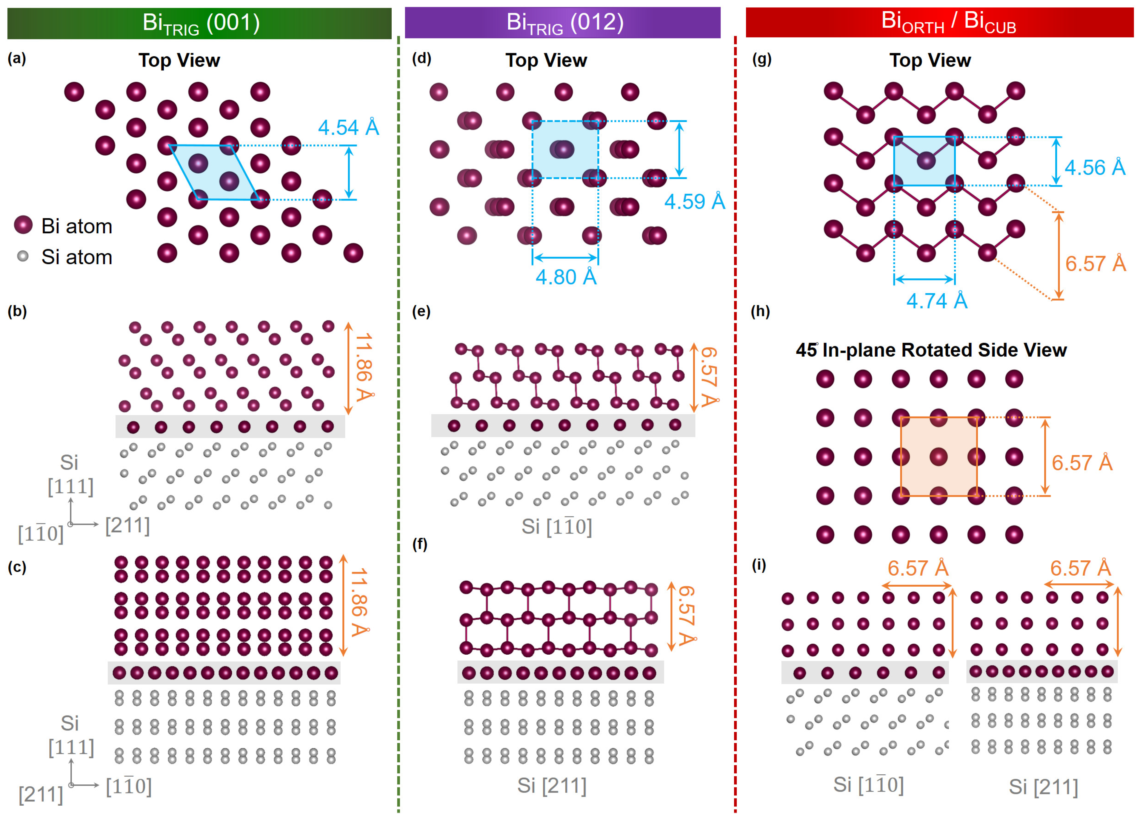
ORTH allotropes are identified. Previous studies have encountered challenges in distinguishing between different nanofilm allotropes of bismuth, leading to uncertainties in characterization. Thin films of some phases exhibit almost identical top surfaces, whereas they significantly differ in the in-plane structure. An overview of crystal structure, depicting the top and cross-sectional side-facets of all attained allotropes in this work, is presented in
Figure 1, where the similarity between Bi
TRIG and Bi
ORTH top-surfaces cannot be ignored. As most of the reported characterizations are based on top-surface investigations, including STM/STS [
13,
16,
20,
21,
29], AFM [
15] and LEED [
22,
27], the differentiation between various phases is challenging and somewhat vague. By conducting in-depth in-plane structural investigations on both single- and polycrystalline epilayers, this study offers a comprehensive understanding of domain alignment in different phases, effectively resolving any ambiguity in distinguishing between Bi
TRIG and Bi
ORTH phases. Taking earlier reports on Bi nanofilm allotropes into account, several unsolved questions regarding the possibility of phase segregation, phase stability, phase transformation, and phase-dependent thickness limitations are systematically exploited and addressed in this study.
In addition to the opportunities this study creates for exploring topological devices, the optimized growth techniques developed in this research hold the potential to benefit a wide range of other fields as well. Topologically trivial Bi undergoes an electronic transition from a semimetal to a semiconductor through quantum confinement [
30,
31,
32]. In its semiconducting regime, Bi can be exploited in quantum sensors [
33] or used as a ferroelectric [
15]. Additionally, due to its poor thermal stability, Bi is a suitable candidate for phase-change applications where the crystalline Bi film can be transformed into an amorphous state with relatively low applied energy [
34]. The thermal instability of Bi
TRIG and ferroelectric attributes of Bi
ORTH designate Bi, in either phase, as one of the most promising candidates for low-power neuromorphic applications. Overall, we are confident that the results of this study will provide the respective communities with significant insight into how to prepare high-quality and phase-segregated crystalline epilayers, so that Bi in the required phase can be readily incorporated into the respective device platforms in a scalable manner.
2. Growth Optimization and Characterization of BiTRIG
Single-elemental thin films entail an immensely diverse temperature range to crystalize in certain phases. Some elements demand ultra-low temperatures (below 0 °C) to crystallize, such as Al and Sn [
35,
36], while others require temperatures as high as 1400 °C, such as Ta. Bi, however, tends to crystallize at room temperature. In order to grow smooth and high-crystal-quality films of Bi via MBE, the optimum growth parameters, i.e., the growth temperature (T
sub) and the thin-film growth rate (R
TF), must be identified.
Initially, to acquire the Bi
TRIG phase, the growth of Bi films is conducted over a T
sub range from −20 °C to 80 °C, where the temperature of the Bi effusion cell is adjusted to maintain R
TF = 10 nm/h. The morphology of the films is analyzed via scanning electron microscopy (SEM), while the structural characterizations are performed via XRD. The X-ray reflectometry (XRR) scans have provided the necessary information about the thickness and roughness of each film. It is observed that films prepared at low temperatures exhibit smoother surfaces, with roughness increasing significantly with increasing T
sub, as can be seen in
Figure 2a. Preliminary XRD investigations have revealed diverse structural behavior of the Bi films, including amorphous, single-, and polycrystalline states over the entire range of T
sub. The results of qualitative investigations of Bi
TRIG crystals, acquired via rocking-curve (RC) analysis of the Bi
TRIG peak, can be visualized in
Figure 2a. A similar set of growths is conducted with an increased R
TF = 15 nm/h, and while a similar trend is observed, there appears to be a slight improvement in surface and crystal quality. The summarized results of this R
TF can be visualized in
Figure 2b.
Based on RC analysis, the investigated temperature range is divided into distinct categories that are named “amorphous”, “high defect density”, “transition”, “optimum” and “deformation” zones. The corresponding temperature zones are highlighted in grey, orange, white, green and red, respectively, in
Figure 2a,b. The Bi films prepared between −20 °C and 0 °C are observed to be either amorphous or partially crystalline and are thus placed in the “amorphous zone”. The films prepared between 0 °C and 15 °C are witnessed to be crystalline in the Bi
TRIG phase; however, these films exhibit a poor crystal quality with RC full-width-half-maxima (FWHM) values above 900″. This temperature range is thus categorized as the “high defect-density zone”. The average grain size and henceforth, the crystal quality is observed to improve continuously throughout the “transition zone” between 15 °C and 35 °C, with the RC values reaching close to 300″. The films prepared in the “optimum zone” with T
sub ranging between 35 °C and 50 °C are observed to have the best crystal quality where RC values below 200″ are achieved. Above 50 °C, epilayers are observed to degrade in structural quality, as seen by the increase in RC, and the crystal is observed to transform into a polycrystalline state. This occurs due to an increased density of point and structural defects. This increase in defect density arises as the epilayer becomes more and more thermally unstable with increasing T
sub. This temperature range is thus categorized as the “deformation zone”. With the identification of the “optimum zone”, T
sub = 40 °C is witnessed to deliver the best results and, therefore, is selected for all future growths of the Bi
TRIG phase. The focus is then shifted to the identification of optimum R
TF. As witnessed in
Figure 2a,b, compared to R
TF = 10 nm/h, both features, i.e., the surface and crystal quality, are observed to improve at R
TF = 15 nm/h. It points toward a higher probability of achieving optimum growths at R
TF > 15 nm/h. Following that, several Bi
TRIG epilayers are prepared where R
TF is gradually (in steps of 2 nm/h) increased from 10 nm/h to 30 nm/h, while T
sub is kept constant at 40 °C. The corresponding changes in the surface morphology can be observed via SEM images. A few images, corresponding to key R
TF values, are depicted in
Figure 2c–h. Through the SEM images, a substantial improvement in the surface quality of the epilayers is observed with increasing R
TF. Not only do the Bi crystallites seen at lower R
TF vanish, but the averaged grain size is also observed to enlarge significantly. Though epilayers are prepared with R
TF up to 30 nm/h, the best results are obtained at R
TF = 22 nm/h, and thus, this is selected as the optimum R
TF.
With the optimal growth parameters (T
sub, R
TF) = (40 °C, 22 nm/h) for the Bi
TRIG phase found, several epilayers with various thicknesses are prepared to confirm the growth reproducibility by analyzing the surface roughness and crystal quality of each epilayer. After confirming reproducible growths, detailed structural characterizations are performed via XRD, and the lattice parameters of Bi
TRIG epilayers are evaluated.
Figure 3a represents the measured XRR and simulated curves of a 16 nm thick epilayer. The fitting parameters confirm the ultra-smooth surface, where the measured roughness is even better than the Si
substrate itself, which is not something one would expect in MBE. The reason for achieving such an ultra-smooth epilayer resides purely in the structural arrangement of Bi
TRIG. As introduced in
Figure 1, the Bi
TRIG crystals are arranged in vertically stacked bilayers where the height of a single bilayer (3.9 Å) matches almost perfectly with the Si step-edge height (3.87 Å) [
5,
6]. It is known that Si step edges act as nucleation sites in an early stage of growth [
37]. However, during the growth of layered materials such as Bi
2Te
3 and Sb
2Te
3, these step heights lead to the formation of extended structural defects, including antiphase domains and screw dislocations [
5,
6], whereas, in the case of Bi
TRIG, a bilayer with matching height inserts itself at the step edge, neutralizes the formation of extended defects, and results in an improved crystal and surface quality of the epilayer.
Figure 3b represents an XRD
scan confirming the single crystalline behavior of the Bi
TRIG epilayer. It is also due to the acquired ultra-smooth surface that the thickness oscillations are observed to appear all the way up to 60° in the diffraction pattern.
Ensuring the single crystallinity of the epilayer, the qualitative investigations are performed via RC
analysis at the Bi
TRIG peak.
Figure 3c depicts the measured RC and the corresponding Gaussian fit, providing the FWHM value of 53 ± 10″. To the best of our knowledge, such a low FWHM value in the MBE-grown Bi-based materials has never been reported. Finally, the lattice parameters are evaluated using the symmetric and asymmetric reciprocal space maps (RSMs).
Figure 3d represents a symmetric map across the Bi
TRIG peak. The measured value provided
= 2
(2.529) ± 0.002 nm
−1 = 1.588 ± 0.002 Å
−1 which results in an out-of-plane lattice “c” = 11.86 ± 0.01 Å. This acquired value matches perfectly with the reported value in the literature, as mentioned in
Figure 1a. It is worth mentioning here that the acquired
value is zero, and thus, any information about the in-plane lattice cannot be extracted. In symmetric setting, x-rays probe only the vertical lattice and provide high-precision information only about the out-of-plane parameter. It, however, lacks any information about the in-plane structure. Depending on material composition and crystal symmetry, XRD peaks differ in their intensity. Considering the Bi
TRIG phase, the asymmetric
peak is selected to probe the in-plane structure, and the lattice information is extracted. The corresponding RSM is depicted in
Figure 3e. As both in-plane lattices are identical (trigonal structure), a single asymmetric peak is sufficient to evaluate the lattice information.
3. Structural Transformation and Phase Map
With the successful growth of Bi
TRIG epilayers, the focus is shifted to the earlier introduced “deformation zone”. As stated in
Figure 2, the crystal is observed to exhibit a polycrystalline state when exposed to T
sub > 50 °C. Preliminary XRD investigations indicated that it is either the Bi
TRIG or the Bi
ORTH phase (as both phases exhibit identical out-of-plane lattices), co-existing with the Bi
TRIG . The existence of Bi
ORTH phase has already been reported in the literature, however, only in the form of non-coalescent ultra-thin (<2 nm) crystallites [
21,
38,
39]. A recent study has reported the presence of 60-nm-wide Bi
ORTH crystal grains reaching the thickness of approx. 25 nm in polycrystalline films [
26]. Thus, the possibility of growing thick Bi
ORTH crystallites is addressed, while the uncertainty of achieving phase-pure, fully coalesced, and high-crystal-quality Bi
ORTH epilayers still remains. These obscurities must be tackled before the incorporation of Bi
ORTH in nano-devices becomes a reality.
Considering the significance of Bi
ORTH to neuromorphic, ferroelectric, and topological communities, a systematic search for the Bi
ORTH phase is initiated. Keeping R
TF at the optimum value of 22 nm/h, adopted for the Bi
TRIG phase, a series of growths are conducted where T
sub is gradually (in steps of 2 °C) increased from 40 °C to 120 °C. The structural investigations are performed, and a summary of the acquired results is plotted in
Figure 4a.
Figure 4b represents the diffraction pattern at select key data points, and
Figure 4c–h depict the corresponding morphological alterations via SEM images. At low temperatures, the surface roughness is observed to increase gradually until T
sub reaches 70 °C, after which a rapid increment in the surface roughness is evident. This behavior can also be witnessed in
Figure 4b with the vanishing thickness oscillations in the corresponding diffraction patterns. The crystal quality of the Bi
TRIG phase is observed to continually degrade with increasing T
sub, as can be seen with the increasing FWHM values in
Figure 4a. After T
sub = 55 °C, the Bi
ORTH phase started to emerge, initially with a poor crystal quality that continually improved with increasing T
sub until 105 °C. For better understanding, the earlier designated “deformation zone” in
Figure 2 is dissected into further sub-groups. In the region from T
sub = 55 °C to 95 °C, only polycrystalline layers (containing both the Bi
TRIG and the Bi
ORTH phases) are achieved. Due to the continually decreasing fraction of Bi
TRIG and increasing ratio of Bi
ORTH, this region is named the “transformation zone”. Above the transformation zone, a small set of temperatures, i.e., 95–105 °C, have provided the pure phase of the Bi
ORTH crystals. Though the surface quality of acquired Bi
ORTH is far from optimal, the crystal quality is at an acceptable level, with the FWHM value of the Bi
ORTH peak reaching below 300″. This region is designated the “optimum zone (orthorhombic)”. Above this temperature, the crystal is only observed to degrade, thus starting the actual “deformation zone”.
Before the focus is shifted to optimizing the surface quality of Bi
ORTH crystals, a couple of points are worth mentioning here. (1) For the first time, phase-pure growth of Bi
ORTH crystals having a thickness >> 2 nm is successfully achieved via MBE. (2) Though Bi
ORTH peaks started to emerge at T
sub > 55 °C, a sudden change in crystal morphology and structural alignment is observed to transpire in the transformation zone between 70 °C and 80 °C. Referring to
Figure 4e,f, the presence of a relatively smooth and almost fully coalesced layer at 70 °C is suddenly converted into rough and randomly ordered crystals at 80 °C, confirming a sudden rather than a gradual change in the crystal structure. Moreover, notice the change in XRD pattern between 70 °C and 80 °C in
Figure 4b, where a clear indication of contributing layer thickness change can be perceived. The preliminary characterizations of the in-plane structure indicate that from 55 °C to 70 °C, the peak appearing at
= 27.2° belongs to the Bi
TRIG phase, and not the Bi
ORTH. Above 70 °C, however, the crystal re-arranges itself, undergoes a few transformations, and converts into the Bi
ORTH phase that slightly differs from the Bi
TRIG orientation. It is interesting to note that the out-of-plane lattices in Bi
TRIG and Bi
ORTH match perfectly, and this is the reason that no significant shift in the diffraction peak is observed. At this stage, it can be assumed that the Bi
TRIG orientation acts as an intermediate stage between Bi
TRIG and Bi
ORTH phases. Further discussions on similarities and differences between both phases, i.e., the Bi
TRIG and the Bi
ORTH, will be conducted at a later stage; however, right now the focus will be kept on the surface optimization of the Bi
ORTH phase.
Based on the analysis of
Figure 4, it is clear that the Bi
ORTH phase can only be segregated at high temperatures (around 100 °C). What role R
TF plays in the phase segregation of Bi films is still unknown. Furthermore, it is also important to study the impact of R
TF on surface quality to achieve smooth and fully coalesced Bi
ORTH epilayers if possible. To answer these questions, a detailed and systematic growth study of Bi films is conducted where T
sub is altered in steps of ±2 °C between the two identified “optimum zones” depicted in
Figure 4a. R
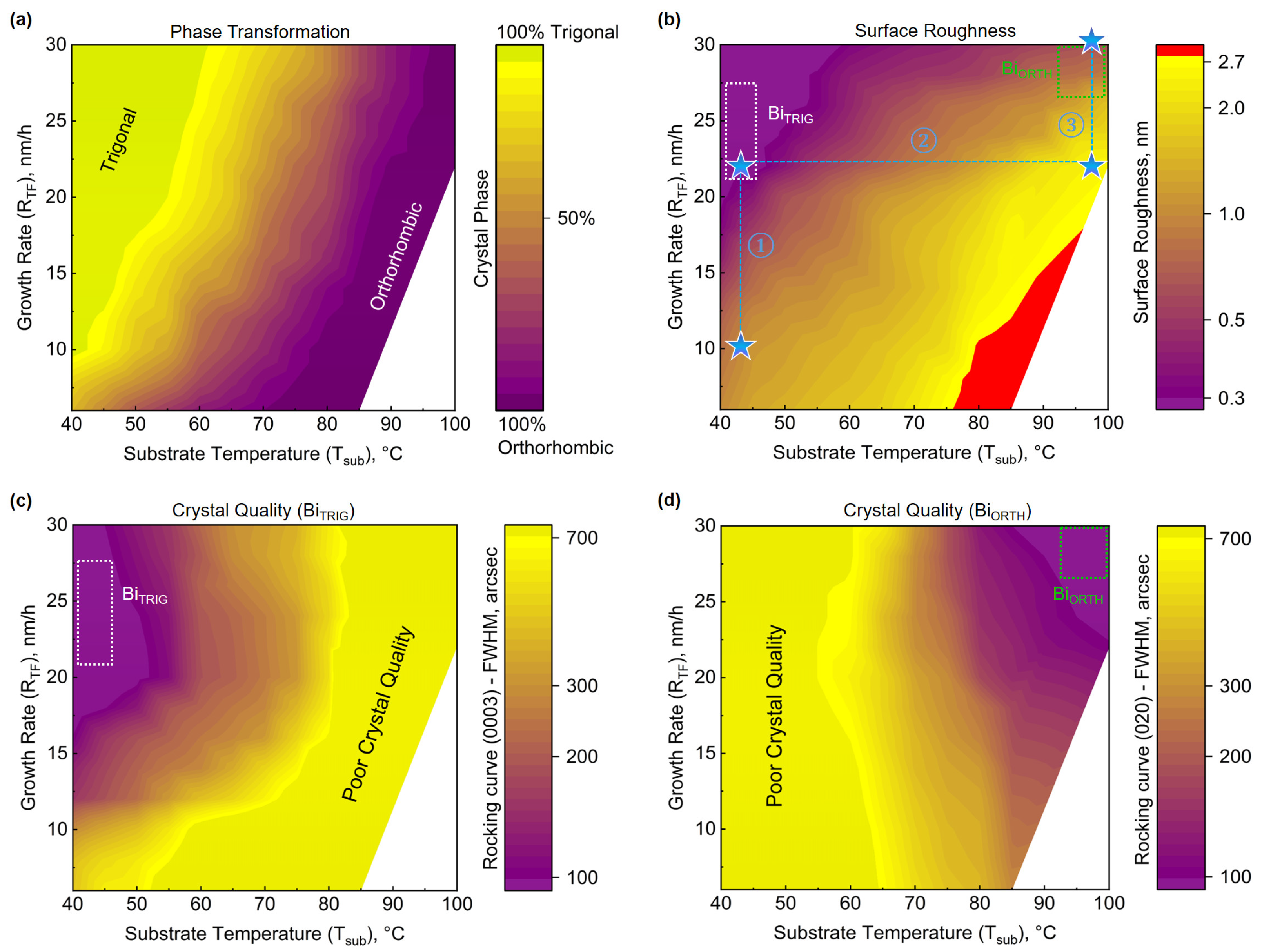
TF is also adjusted in steps of 2 nm/h, starting from 6 nm/h to 30 nm/h. All of the prepared films are investigated via XRD, and the information about crystal phase, crystal quality, and surface roughness is evaluated and depicted with the help of colored maps in
Figure 5.
The impact of growth parameters (T
sub, R
TF) on the crystal phase can be visualized in
Figure 5a. To identify the presence of a single phase in the epilayer is straightforward; however, the question arises as to how to distinguish the relative presence of a specific phase in the polycrystalline films. To understand the impact of changing growth parameters, phase-specific diffraction peaks, i.e., Bi
TRIG and Bi
ORTH , are selected. The measured peak intensities in the diffraction pattern, belonging to a specific film thickness, are multiplied with the corresponding theoretically predicted intensities. The ratio
is evaluated and utilized to identify the relative presence of a certain phase in the epilayer. Similarly, the corresponding information at each data point about the surface roughness and crystal quality, RC-FWHM, for Bi
TRIG and Bi
ORTH peaks is represented in
Figure 5b–d, respectively.
It can be clearly observed that low T
sub and high R
TF facilitate the achievement of the Bi
TRIG phase. Conversely, at high T
sub and low R
TF, films crystallize only in the Bi
ORTH phase. However, none of the above-mentioned parameters are optimal. For Bi
TRIG, high R
TF results in smoother films, as can be witnessed in
Figure 5b; however, after a certain point, the crystal quality starts to degrade with increasing density of rotational domains and reduced grain size, resulting in enhanced RC-FWHM values that can be visualized in
Figure 5c. The best crystal quality is achieved at R
TF between 22 and 26 nm/h. The optimum growth zone for Bi
TRIG is highlighted with the white-dotted box in
Figure 5b,c. As far as the Bi
ORTH phase is concerned, films achieved at low R
TF values exhibit enormously high surface roughness due to the formation of non-coalescing crystallites. Such films are not suitable for integration into any electronic device. With increasing R
TF, the surface roughness is witnessed to improve significantly; however, the temperature requirements to keep the Bi
ORTH phase segregated increase as well. Epilayers with the best crystal quality and improved surfaces of the Bi
ORTH phase are achieved at high T
sub and R
TF values, a region marked with the green-dotted box in
Figure 5b,d.
Observing the phase transformation map, it is evident that almost 80% of the data points resulted in the formation of polycrystalline films. It emphasizes the importance of identifying phase-specific optimum growth zones. Moreover, the achievement of pure-phase and thick crystalline films of the Bi
ORTH phase has not been reported to date. Thus, the transformation maps depicted in
Figure 5 not only helped in achieving phase-pure epilayers of Bi
ORTH systematically, but also provided a platform that serves as a reference for all future requirements of phase-segregated growths of Bi nanofilm allotropes. To highlight the importance of these maps, the path of parameter selection in this study is retraced in
Figure 5b, which leads to the next step, i.e., the surface optimization of Bi
ORTH films.
5. Domain Alignment of Bi Nanofilm Allotropes
To comprehend the in-plane alignment of domains with respect to the substrate, the rotational symmetry of lattices via conventional
-scanning is investigated.
Figure 7 represents detailed information on domain alignment in various Bi phases. A trigonal lattice exhibits 3-fold rotational symmetry. While growing a trigonal crystal on a hexagonal surface, e.g., Si
, the crystal may exhibit 60° in-plane rotated domains. A similar scenario is observed in Bi
TRIG epilayers, as depicted in
Figure 7a. The figure on top is a 3D pole-figure map, acquired via probing the Bi
TRIG peak to identify all present domains in the epilayer, as this peak exhibits the highest diffraction intensity. It is evident that the epilayer contains twin domains, i.e., 60° rotated domains that can also be visualized with the help of an illustration containing two 60° rotated colored triangles placed inside the pole-figure map. Moreover, the domains are observed to be collinear with the substrate peak, referring to the 60°, 180°, and 300° marks in the map. At the bottom of
Figure 7a, a 2D cut at
χ = 55.7° is plotted. From the intensity, it is evident that both rotational domains have not populated the epilayer equally; rather, a 1:5 ratio is observed. Other trigonal crystals, e.g., Bi
2Te
3 and Sb
2Te
3, are also reported to exhibit a similar trend when grown on Si
[
5,
6]. However, in the case of Bi
TRIG, a minor difference is perceived. It is observed that the Bi
TRIG exhibits a preferential alignment to Si
, which is a behavior opposite to that of Bi
2Te
3 and Sb
2Te
3 crystals that favor Si
instead. Why Bi
TRIG behaves differently from other family compounds is not clear at this point and requires further insight with the support of theoretical modeling. Nevertheless, a similar trend is observed in all Bi
TRIG epilayers prepared at T
sub from 5 °C to 50 °C, while R
TF > 10 nm/h.
During this investigation, it was discovered that for T
sub > 50 °C, the crystal enters the “transformation zone” where unique in-plane transitions are observed, as visualized in
Figure 7b. The 60° rotated domains of Bi
TRIG are highlighted with green-colored regions. Starting from T
sub = 54 °C, distinctive three-pointed peaks start to emerge in between Bi
TRIG domains. These domains, similar to the Bi
TRIG, are observed to exhibit 60° periodicity; however, their alignment in between the Bi
TRIG peaks placed them at a 30° offset with the substrate collinearity. These domains are highlighted with purple-colored regions in
Figure 7b. Alongside the appearance of exotic three-pointed peaks in the
-scan, a diffraction peak at
= 27.2° is witnessed to emerge, as discussed in
Figure 4b, which confirms that these two events are linked. Moreover, as the exotic peaks in the
-scan exhibit 60° periodicity, they cannot originate from the Bi
ORTH phase and must be connected to the Bi
TRIG orientation, as the Bi
TRIG also exhibits the facilitating diffraction peak at
= 27.2°. This assumption, however, requires further investigation. With increasing T
sub, the relative intensity of these uniquely oriented peaks is also observed to rise until T
sub = 70 °C.
Above 70 °C, another in-plane transition is witnessed where each three-pointed exotic peak is observed to split into two distinct peaks that are 30° apart from each other and ±15° shifted from the position of their origin, highlighted by the black-dotted arrows in
Figure 7b. Thus, the newly originated peaks exhibit a 45° offset from the substrate collinearity. This transition gives rise to 12 peaks that exhibit 30° periodicity, along with six peaks originating from the Bi
TRIG as observed in an epilayer prepared with T
sub = 75 °C and depicted in
Figure 7b. As far as the diffraction pattern is concerned, no significant change in peak positions is observed. The morphology of the crystal, on the other hand, is observed to transform completely, as discussed in
Figure 4. As the appearance of 12 distinct peaks with 30° periodicity is a hallmark of cubic-like structures when aligned on a hexagonal surface [
40], this second stage of transition can be linked to the rise of the Bi
ORTH phase.
With further increase in T
sub, peaks associated with the Bi
TRIG are witnessed to diminish, while 30° periodic Bi
ORTH peaks are observed to improve in intensity until T
sub reaches 95 °C. Above 95 °C, epilayers are observed to crystallize in the Bi
ORTH phase only.
Figure 7c depicts a 3D pole-figure map of the Bi
ORTH epilayer acquired via probing
peak and a 2D cut at
= 57.9°, confirming the presence of only 12 in-plane peaks. As the orthorhombic lattice exhibits four-fold rotational symmetry, the alignment of domains in the epilayer is illustrated with the help of three distinct colored boxes rotated by 30° and placed inside the pole-figure map. The four-fold rotational symmetry can also be witnessed in a 2D
-scan where each peak is color-identified with the associated domain. During the first and second in-plane transitions in
Figure 7b at 54 °C and 75 °C, respectively, the non-collinearity of the crystal peak with respect to the substrate was explained. Here, all three Bi
ORTH domains can be visualized to exhibit a 15°, 45°, and 75° offset with respect to the substrate peak, respectively.
Through detailed analyses of
-scans, it can be summarized that from the “optimum zone (trigonal)”, i.e., (T
sub, R
TF) = (40 °C, 22 nm/h), to the “optimum zone (orthorhombic)”, i.e., (T
sub, R
TF) = (100 °C, 32 nm/h), epilayers go through four major states. (1) All epilayers before entering the “transformation zone” exhibit twin domains with six distinct peaks originating from the Bi
TRIG phase. (2) Epilayers prepared at 50 °C < T
sub ≤ 70 °C exhibit polycrystalline structures featuring the Bi
TRIG along with the Bi
TRIG orientation. The exotic three-pointed peaks are found to be related to the Bi
TRIG orientation, which is confirmed via asymmetric RSM that can be seen in
Supplementary Figure S1. (3) Epilayers prepared at 70 °C < T
sub < 95 °C also exhibit polycrystalline structures; however, here, the Bi
TRIG and the Bi
ORTH phases are realized. As the out-of-plane lattices in the Bi
ORTH and the Bi
TRIG orientations match with good approximation, no significant change in the diffraction pattern is observed (
Figure 4b). The signature 12 peaks of orthorhombic crystal along with six peaks of the Bi
TRIG are observed in this region. It is also important to point out here that, for a short temperature range, epilayers are also witnessed to contain all three phases, including Bi
TRIG , Bi
TRIG and Bi
ORTH . As the temperature range to host these three phases is very narrow,
-scans are not presented in
Figure 7. (4) Finally, the phase-pure Bi
ORTH epilayers are acquired at T
sub ≥ 95 °C, where only 12 distinct peaks of three rotational domains are observed in the epilayer.
6. Evaluation of Lattice Parameters of BiORTH
After a thorough understanding of domain alignment in the various Bi phases, the focus is set to evaluate the 2D in-plane lattices of Bi
ORTH using asymmetric RSMs. Based on reported Bi
ORTH lattices [
21,
26], the Bi
ORTH and the Bi
ORTH peaks are probed (details can be found in
Supplementary Figures S2–S4), and unexpectedly, no diffraction is observed. It indicates the selected lattice parameters are incorrect. After several failures to probe individual in-plane lattices, successful diffractions are finally achieved for 45° rotated the Bi
ORTH and the Bi
ORTH peaks, and, as expected (orthorhombic crystal, unlike cubic, exhibits nonequivalent in-plane lattices), dual diffraction peaks are detected. These peaks contain information about both in-plane lattices but are not ideal for extracting lattice information as they have reduced diffraction intensity. Nonetheless, by probing these peaks, the diffraction is successfully witnessed for each 30° rotated domain, as explained in
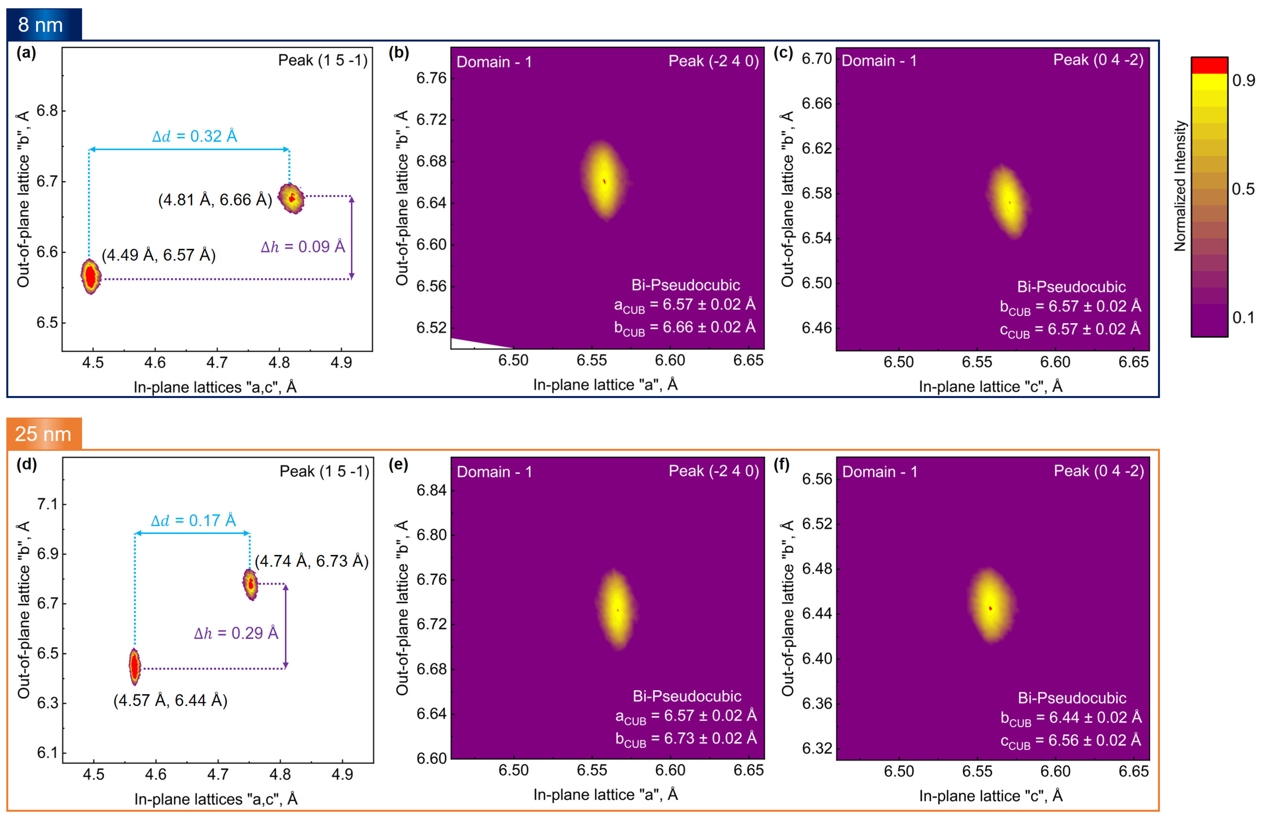
Figure 7c. One of the asymmetric RSMs acquired at the Bi
ORTH peak is depicted in
Figure 8a, where the in-plane lattice parameters are found to be 4.49 ± 0.02 Å and 4.81 ± 0.02 Å, respectively. The measured lattices are in close agreement with reported values of Bi
ORTH on HOPG [
10,
13,
39], but they differ slightly from reported values acquired on Si
[
21,
26,
27,
29,
41].
Analyzing RSM in
Figure 8a, it can be seen that both in-plane lattices are unequal, having a difference of
= 0.32 Å. Moreover, a minute difference along the z-direction of both peaks is also evident and is measured to be
= 0.09 Å, which can be related to buckling [
13,
15,
29]. Buckling is a strain-induced deformation in a crystal and can be described as the height difference between two atoms of the same monolayer [
13]. During the lattice transformation of Bi
TRIG, a phase known to exhibit strong buckling, into Bi
ORTH, the strain relaxation in the crystal modifies the buckling height to reduce it. In this work, the measured buckling of 0.09 Å affirms the relaxed state of Bi
ORTH in comparison to Bi
TRIG [
13,
15,
21]. Almost all studies on Bi
ORTH have reported buckling to be present, and the extent of buckling is reported to have a huge influence on the topological properties [
10,
13,
15,
21]. According to Lu et al., the measured value of buckling height, i.e., 0.09 Å in this work, places Bi
ORTH crystals in a topological regime [
13].
Though in-plane lattices are successfully measured, there remains a question of why the diffraction is not observed for conventional high-intensity peaks, i.e., the Bi
ORTH and the Bi
ORTH , while a low-intensity peak such as the Bi
ORTH is probed successfully. The answer resides in the unique structural arrangement of the Bi
ORTH crystal on Si
substrates. The 45° in-plane rotation of the Bi
ORTH lattice, when projected on Si
and Si
planes, together with the matching out-of-plane lattice, facilitates the formation of a pseudo-cubic sub-lattice, as depicted in
Figure 1g–i. To date, RSM-based structural investigations of the Bi
ORTH phase have not been reported, which presented certain challenges in the evaluation of diffraction peaks. Nonetheless, based on the values evaluated by the Pythagorean theorem stated in Equations (1)–(3) and the matching out-of-plane lattice parameters, Bi in a pseudo-cubic structure (Bi
CUB) is estimated to arrange itself with “a” ≈ “b” ≈ “c” ≈ 6.57 Å. Adopting Bi
CUB parameters, high-intensity asymmetric peaks are selected, and asymmetric RSMs at the Bi
CUB and the Bi
CUB peaks are successfully acquired, as shown in
Figure 8b,c respectively. The difference in the out-of-plane lattices acquired via the Bi
CUB and the Bi
CUB can be linked directly to the Bi
ORTH in
Figure 8a. In other words, the Bi
ORTH and the Bi
CUB are two different representations of the same crystal structure. To confirm the lattice symmetry, RSMs at the Bi
CUB and the Bi
CUB peaks are also acquired for 30° and 60° rotated domains, and similar results are attained that can be visualized in
Supplementary Figures S5 and S6.
During RSM investigations, it was observed that thickness plays a critical role in the structural arrangement of the Bi
ORTH lattice. RSMs acquired at the the Bi
ORTH peak in a 25 nm thick epilayer are depicted in
Figure 8d, where the in-plane lattice parameters are found to be 4.57 ± 0.02 Å and 4.74 ± 0.02 Å, respectively. It is evident that both in-plane lattices have shifted slightly, and the difference between them
is reduced from 0.32 Å to 0.17 Å. Moreover, the buckling height is witnessed to enhance three-fold, from 0.09 Å to 0.29 Å, when the layer thickness is increased from 8 nm to 25 nm, indicating the increased strain in the Bi
ORTH crystal. A similar effect is also observed by measuring the Bi
CUB and the Bi
CUB peaks depicted in
Figure 8e,f, respectively, confirming the enhanced buckling height in the thick Bi
ORTH film. An interesting point to mention here is, that, no thickness dependent change in the in-plane lattices of Bi
CUB is observed. It is due to the fact that the projected values of both sets of orthorhombic lattices at 8 nm (
Figure 8a) and 25 nm (
Figure 8d) remain almost identical (Equation (3)). The acquired lattices in a 25 nm-thick Bi
ORTH epilayer are found to be in close agreement with earlier reports on Si
, although the buckling height is still much smaller than the reported value of 0.5 Å [
21,
26,
27,
29,
41].
7. Atomic-Scale Structural Characterization
Finally, using scanning transmission electron microscopy (STEM), atomic-scale structural characterizations of Bi nanofilm allotropes are performed. Epilayers from three distinct phases, including the Bi
TRIG, the Bi
ORTH , and a polycrystalline phase acquired at T
sub = 70 °C containing both the Bi
TRIG and the Bi
TRIG orientations, are selected. The selected epilayers are then probed via focused ion beam (FIB), and lamellae at the cross-sections of each epilayer along Si
and Si
, are extracted. The Bi epilayers, unlike other layered materials, presented serious challenges both in extracting lamellae and in acquiring high-resolution STEM images. On several occasions, the lamellae were observed to be amorphous with a heavily deformed interface at the substrate. A few examples are summarized in
Supplementary Figures S7–S10. Such a behavior can be explained by a poor thermal stability of Bi. By carefully fabricating lamellae at low energies in FIB and reducing the exposure time under the focused electron beam during STEM, successful structural investigations are performed, and the key results are summarized in
Figure 9.
Figure 9a depicts an overview high-angular annular dark-field (HAADF) image of the Bi
TRIG epilayer along the Si
projection. An atomically sharp interface between Bi
TRIG and Si
can be visualized in
Figure 9b,c, depicting HAADF and bright-field (BF) images, respectively. Before the periodic stacking of Bi bilayers, the appearance of a Bi monolayer passivating the dangling bonds at the Si
surface, is evident. It affirms the formation of
—Bi surface, a 2D sheet of Bi, as a seed layer for epitaxial growth of Bi
TRIG. A magnified HAADF image of the central region, away from the interface, is depicted in
Figure 9d, affirming the high structural quality of the epilayer without the appearance of any extended defects.
During the investigation of polycrystalline epilayers, the presence of the Bi
TRIG oriented crystals, predicted during the analysis of domain alignment in
Figure 7b, is successfully observed. A HAADF image focusing on the Bi
TRIG oriented grain is depicted in
Figure 9e, while a low-pass filtered, magnified image of a central region is depicted in
Figure 9f. It clearly indicates a black-phosphorus-like puckered structure of Bi atoms; however, unlike the black phosphorus, the Bi
TRIG exhibits a strong buckling between the Bi atoms that can also be visualized in the image. Atomic distance measurements via line profiles of the HAADF image have revealed the buckling height to vary between 0.43 ± 0.02 Å and 0.48 ± 0.02 Å in a Bi
TRIG monolayer. The difference between various measured values at different positions in the acquired image can be linked to localized changes in the tilt angle as the lamella is witnessed to be heavily bent due to the curtain effect imposed by the deposited Pt layer during FIB. Nevertheless, even the smallest measured value of buckling in the Bi
TRIG orientation is almost half an order larger than the XRD-measured value of buckling in Bi
ORTH thin films, depicted in
Figure 8a.
Figure 9g represents a HAADF image acquired at the cross-section of a Bi
ORTH epilayer along the Si
projection. An apparently relaxed and periodic stacking of the Bi monolayer ordered in a cubic-like structure can be witnessed in the image. An atomically sharp and clean interface between the substrate and the Bi
ORTH epilayer is also evident. As established during XRD investigations, the unique alignment of the Bi
ORTH crystals with a 45° in-plane offset with the Si
substrate facilitates the formation of a pseudo-cubic sub-lattice. A magnified HAADF image depicted in
Figure 9h represents the Bi
CUB structure, with the in-plane and the out-of-plane lattices measured to be 6.57 ± 0.02 Å and 6.44 ± 0.02 Å, respectively. The acquired values from STEM are in good approximation with XRD acquired lattices, depicted in
Figure 8d–f.
8. Thickness-Dependent Phase Transformations
With such a thorough study of Bi epitaxial growth, most of the earlier introduced obscurities regarding nanofilm allotropes are addressed. However, one issue still remains unaddressed: the thickness-dependent phase transformation in Bi epilayers. As mentioned earlier, various reports have confirmed the existence of Bi
ORTH phase during early stages of growth where the Bi
ORTH phase is identified in the form of crystallites not only on Si
but also on Al
2O
3 and HOPG substrates [
10,
13,
15,
16,
27,
29,
39]. According to these reports, the Bi
ORTH phase is observed to be stable in ultra-thin films consisting of up to four monolayers (4ML), approx. 1.3 nm thick. As soon as layer thickness increases, a transformation from Bi
ORTH into Bi
TRIG phase is reported to initiate, which remains true if the layer thickness remains below 8–10 ML (approx. 3.5 nm). However, any film having a thickness > 3.5 nm is reported to crystallize only in the Bi
TRIG phase. These observations are often supported by theoretical modelling and simulations [
21,
29,
41]. The findings in this work mostly contradict the above-mentioned reports, as the epitaxial growths of the Bi
TRIG and the Bi
ORTH phases are performed independently of each other.
However, before releasing a final statement, the dependency of phase transformation on the layer thickness is investigated, and the thickness-dependent controlled epitaxy of both phases, i.e., the Bi
TRIG and the Bi
ORTH , is performed in a systematic manner. The growth parameters are adjusted to the optimum values for the Bi
TRIG, (T
sub, R
TF) = (40 °C, 22 nm/h), and epilayers ranging in thickness from 2.2 nm to 13.5 nm are prepared.
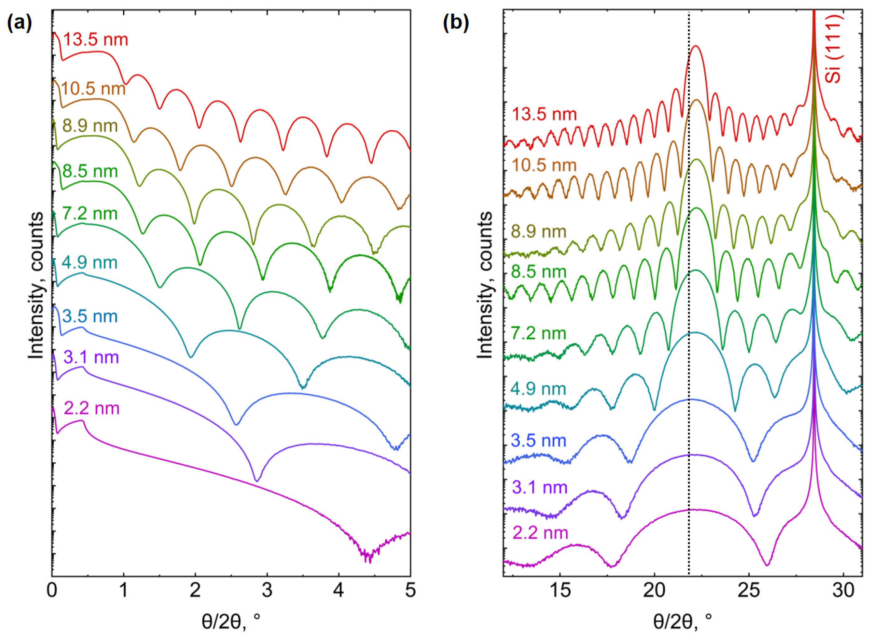
Figure 10 represents the XRD characterization of the Bi
TRIG thickness series, where (a) depicts XRR curves, and (b) depicts the corresponding diffraction patterns. It is evident that all epilayers exhibit only the Bi
TRIG phase, and no indication of phase duality is observed. The black-dotted line highlights a shift in the out-of-plane lattice constant due to the scaling effect. This effect has already been reported for GeTe [
42]; however, it is not discussed here for Bi. As the focus of this work is on the thickness-dependent phase transformation, the investigation of the scaling effect within the same phase is outside the scope of this work. Nonetheless, the growth parameters are then adjusted to the Bi
ORTH optimum values, (T
sub, R
TF) = (100 °C, 32 nm/h), and epilayers in thickness ranging from 1.6 nm to 13.6 nm are prepared. The results are summarized via symmetric RSMs around the Bi
ORTH peak and are depicted in
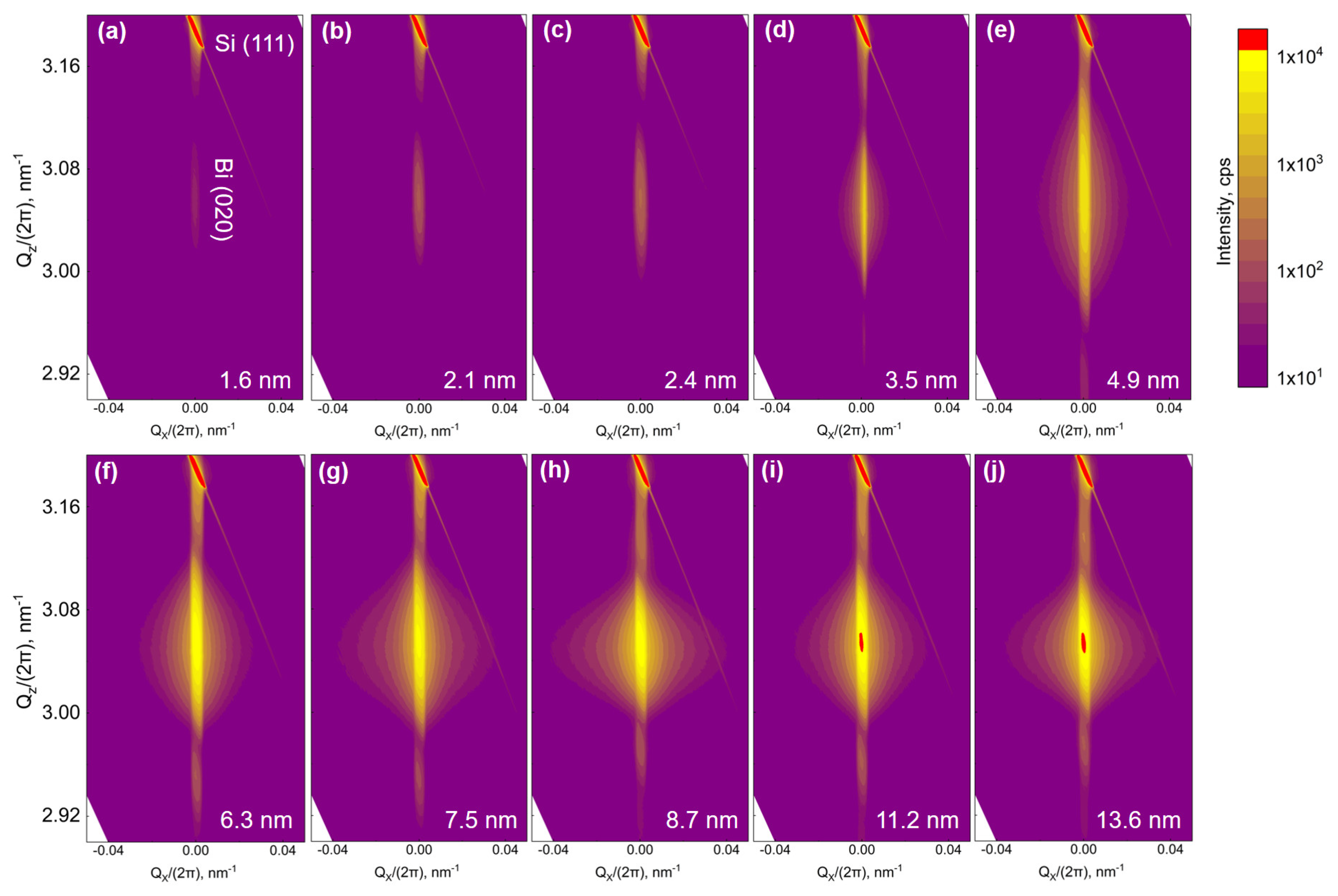
Figure 11.
The presence of the BiORTH peak in layers having a thickness >> 3.5 nm is clear evidence that the BiORTH epilayers can be grown phase-segregated and that layer thickness has no direct relation to phase transformation. Still, it is of critical importance to identify probable factors that may have led to the thickness-dependent phase transformation of BiORTH in earlier-reported studies. The two key differences in this work compared to earlier reports are the substrate surface and the selection of growth parameters. (1) In this work, all growths are performed on Si conventional surfaces passivated by Bi-monolayers, whereas all earlier reports have adopted Si or reconstructed surfaces that may have influenced the starting phase of Bi films. (2) For the first time, phase-dependent optimum growth parameters are evaluated and implemented in this work to affirm the phase purity of the growing epilayer The thickness-dependent phase transformation may be realized if similar growths are carried out with non-optimal parameters, i.e., in the “transformation zone” or at the zone boundary. However, it is just speculation until confirmed.
Though a thickness-dependent phase transformation in the Bi
ORTH epilayers is not realized, a continuous shift in the lattice parameters is observed.
Figure 11 indicates only a slight change in the out-of-plane lattice depending on the epilayer thickness, whereas major changes are perceived in the in-plane structure of Bi
ORTH. It is observed that at low thicknesses, epilayers exhibit a relatively large difference between the in-plane lattice parameters, while the buckling height remains rather small, as witnessed in
Figure 8a. With increasing thickness, the difference between in-plane lattice parameters decreases, whereas the buckling height increases, thus affirming the increasing strain in the epilayer, as depicted in
Figure 8d. The observed trend of buckling height dependency on the Bi
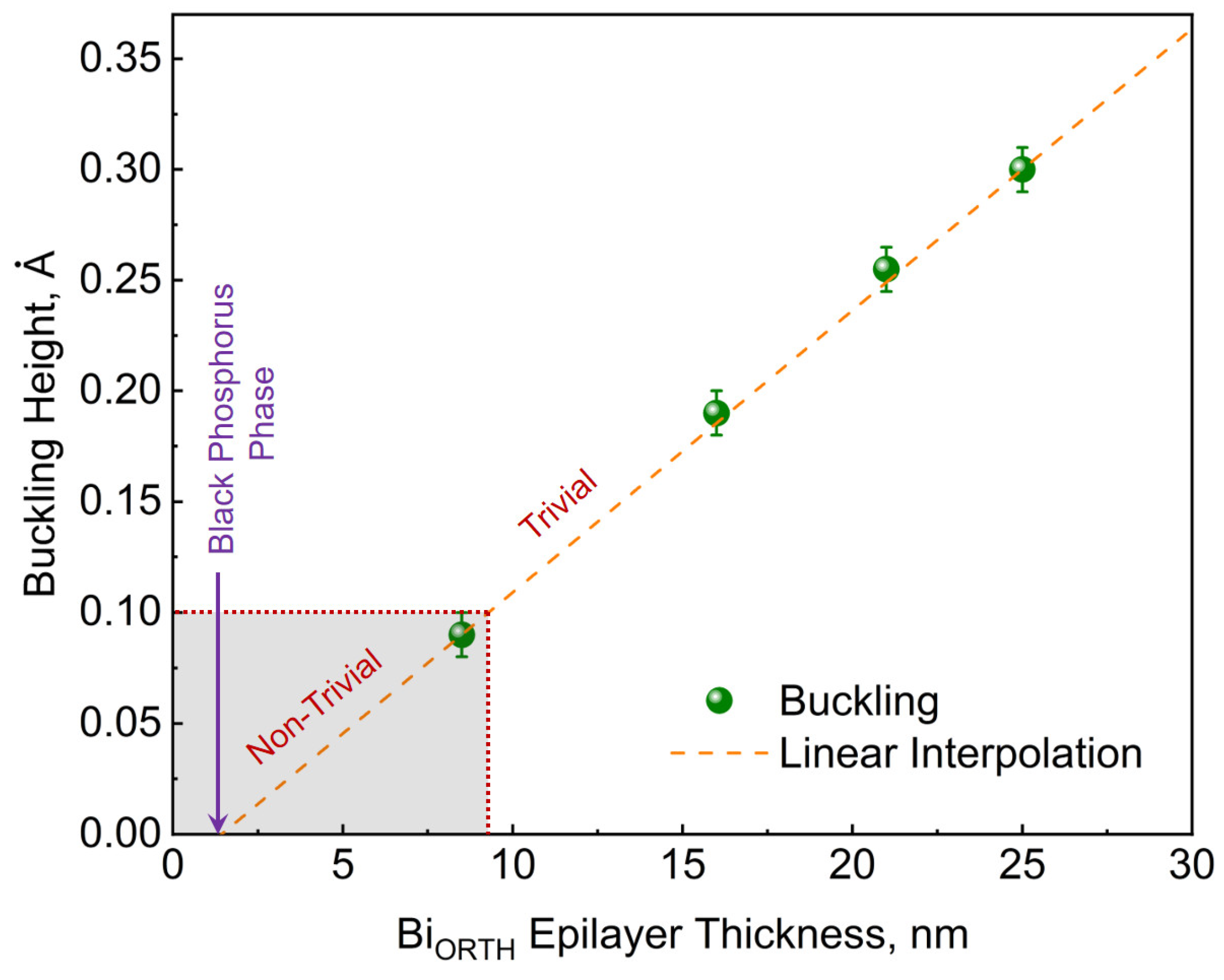
ORTH layer thickness is summarized in
Figure 12. Using linear interpolation, it is identified that the black-phosphorus phase of Bi (Bi
BP) that exhibits zero-buckling can only be realized if the epilayer thickness remains below 1.32 nm. As the thinnest Bi
ORTH epilayer achieved in this work is only 1.63 nm thick, the requirements for realization of the Bi
BP phase are not met, and thus, only the Bi
ORTH phase is observed. The measured buckling values in
Figure 12 also indicate that if such an ultra-thin epilayer is achieved, the probability of realizing the Bi
BP phase is high.
Furthermore, the buckling height is reported to have a huge influence on the topological properties of Bi
ORTH. According to Lu et al., all epilayers with buckling height ≤ 0.1 Å exhibit non-trivial topology, whereas increasing buckling height transforms the epilayer into a trivial phase [
13]. Based on this, all Bi
ORTH epilayers prepared in this work having a thickness ≤ 9 nm must exhibit non-trivial attributes, which was only true for approx. 1.3 nm thick epilayers in all earlier-reported studies. It facilitates the realization of Bi
ORTH-based quantum devices, as the achievement of fully coalesced 9 nm-thick epilayers is far less complex than 1.3 nm. The increasing buckling height in the epilayer indicates that after a certain thickness, the Bi
ORTH epilayer becomes unfavorable and will cross the limit of quantum confinement and transform into the Bi
TRIG phase, just as reported in earlier studies. This hypothesis is confirmed with an attempt to grow a 45 nm-thick Bi
ORTH epilayer, which resulted in a polycrystalline film containing the Bi
ORTH and the Bi
TRIG structures, confirming that the maximum stable thickness of the Bi
ORTH phase is somewhere between 30 nm (depicted in
Figure 9) and 45 nm.
The groundwork for manufacturing nano-devices has now been laid with the successful phase-selective epitaxy of Bi-thin films. However, one must proceed with the utmost caution, as Bi oxidizes quickly when exposed to air. In the initial stages of oxidation, Bi forms a polycrystalline BiO
x layer, as depicted in
Figure 9e. The polycrystalline nature of BiO
x makes it significantly challenging to remove during metallization, and access to a pristine epi-surface to realize atomically clean and sharp interface remains a challenge. A detailed and systematic study of surface oxidation in Bi thin films is performed; however, it is not discussed here as it is outside the scope of this work. Furthermore, due to a low thermal stability, conventional fabrication techniques may degrade the crystal quality of Bi epilayers, which makes it even more challenging to realize functional quantum devices. An earlier-proposed platform with an on-chip stencil mask provides a way around the fabrication challenges [
43], whereas the issue of surface oxidation can be addressed via in situ capping of the epitaxial surface with a passivation layer. Various topological insulator thin films are reported to have successfully achieved surface passivation using an electron beam-deposited thin film of stoichiometric Al
2O
3 [
43,
44,
45,
46]. In some circumstances, a 2 nm thermally evaporated film of elemental Al is adopted as passivation [
47,
48,
49,
50,
51,
52]. Al readily oxidizes and transforms into AlO
x when exposed to air, protecting the underlying surface from deterioration and aging. By combining phase-selective growth of Bi with an on-chip stencil mask [
43] and in situ surface passivation, this study can be used to realize promising quantum devices for a variety of novel topological and neuromorphic applications.


 ,
, 


