
An Optical Technique to Produce Embedded Quantum Structures in Semiconductors

 ,
, 
Abstract
:1. Introduction
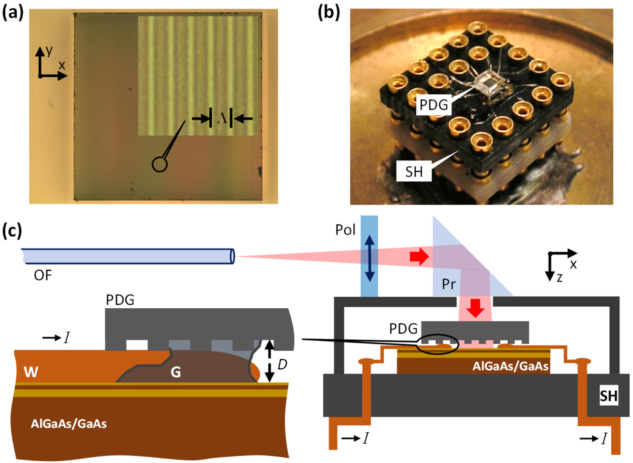
2. Materials and Methods
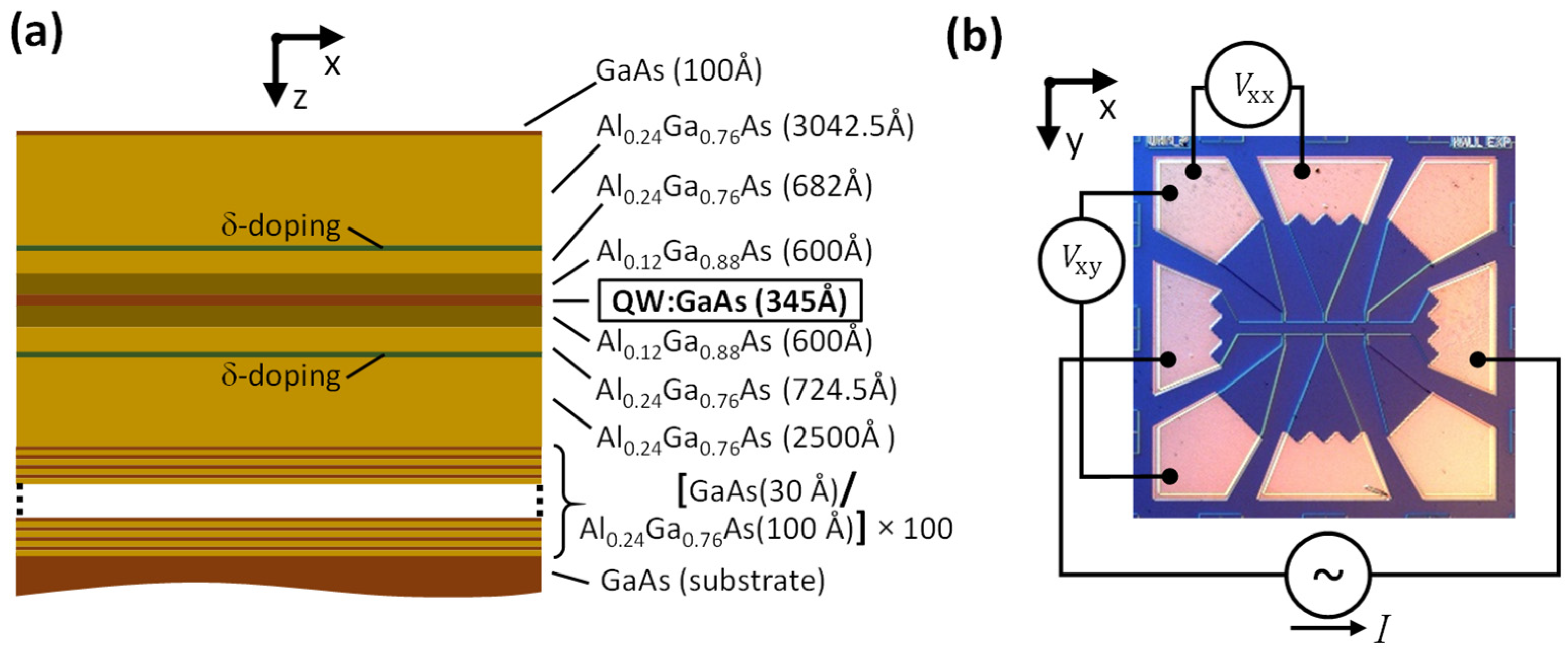
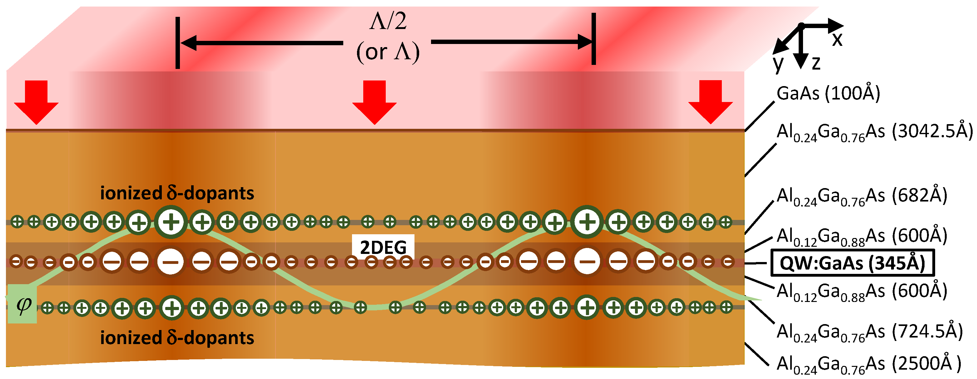
2.1. GaAs/AlGaAs QW-Structure
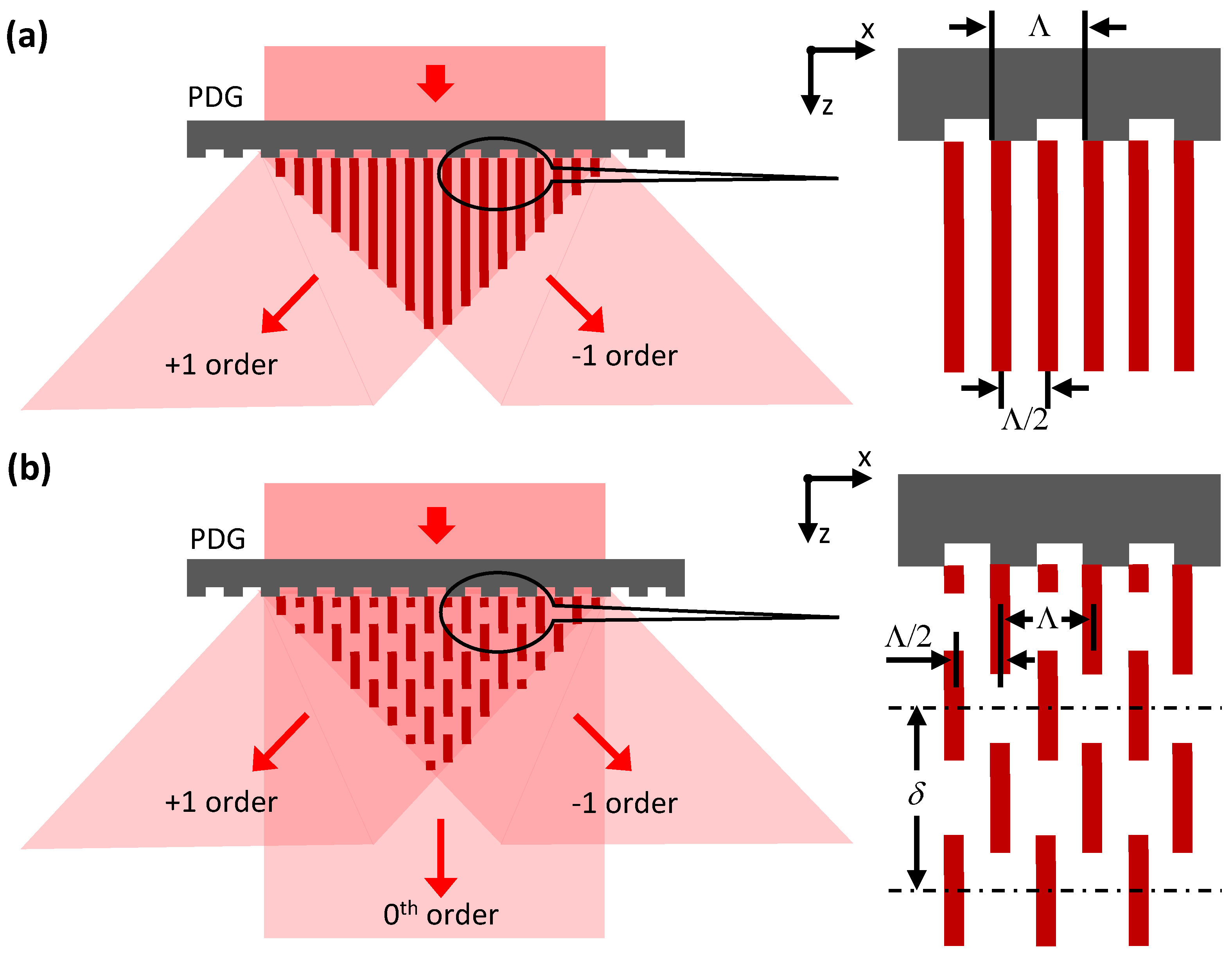
2.2. Light Patterns Generated by PDGs
3. Results
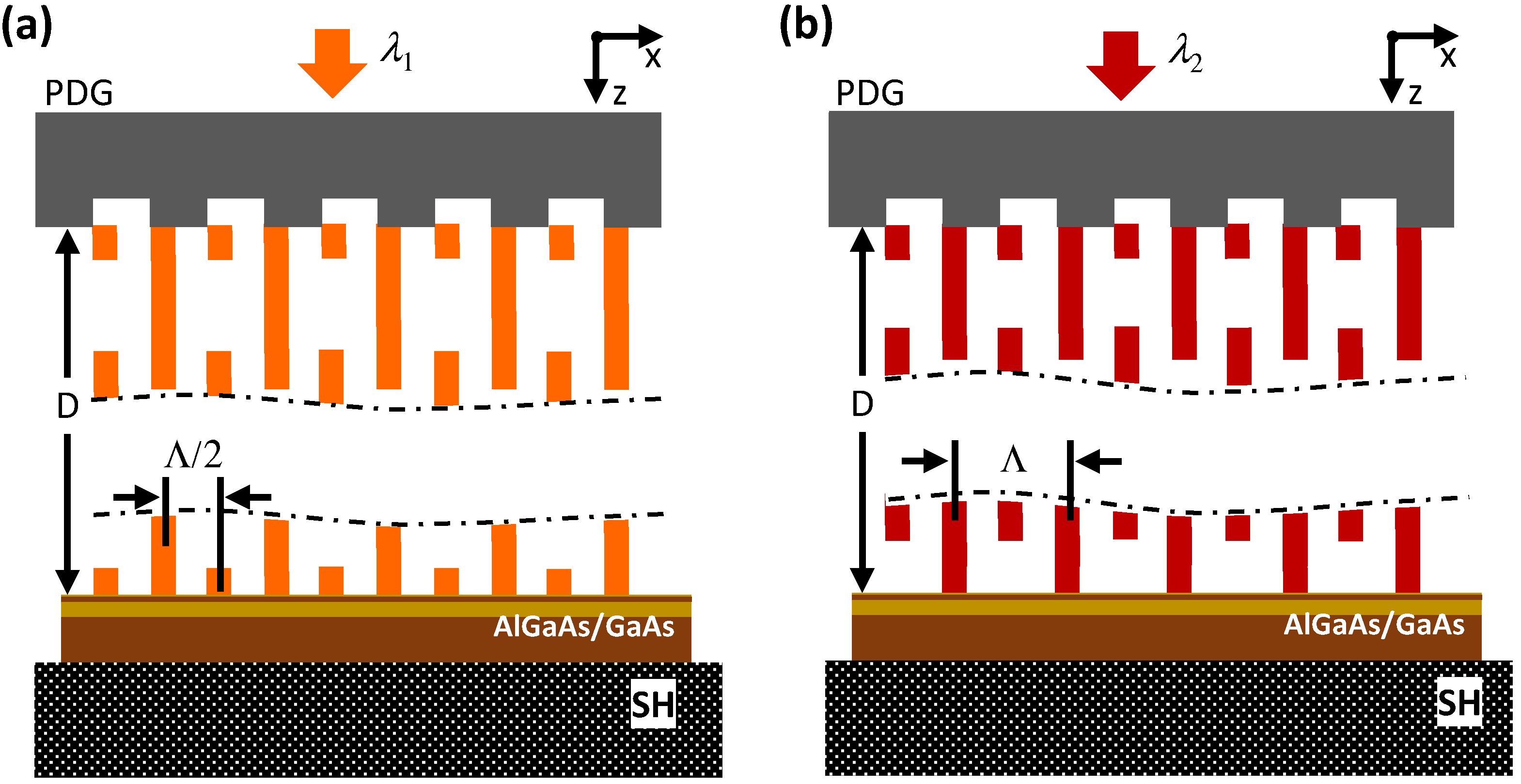
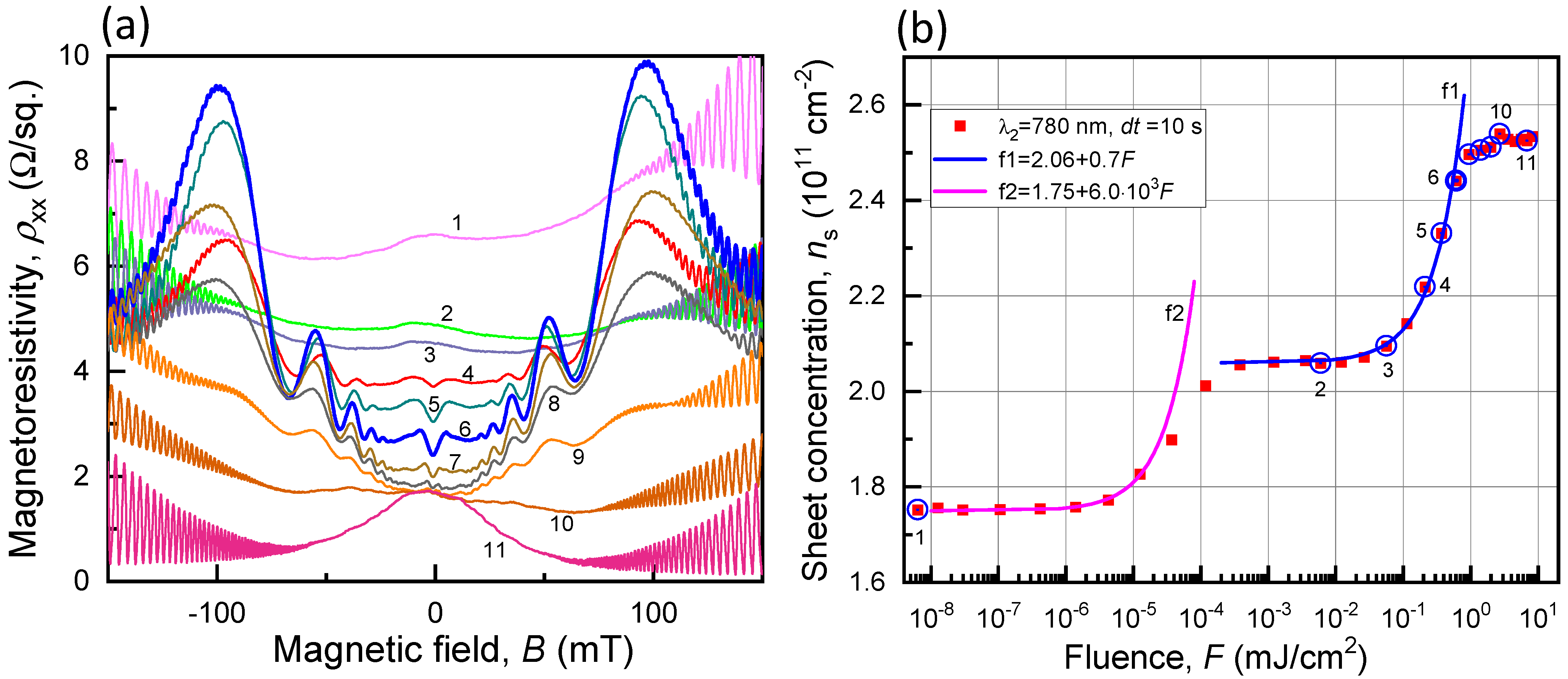
3.1. Hall Bar Illumination at = 780 nm
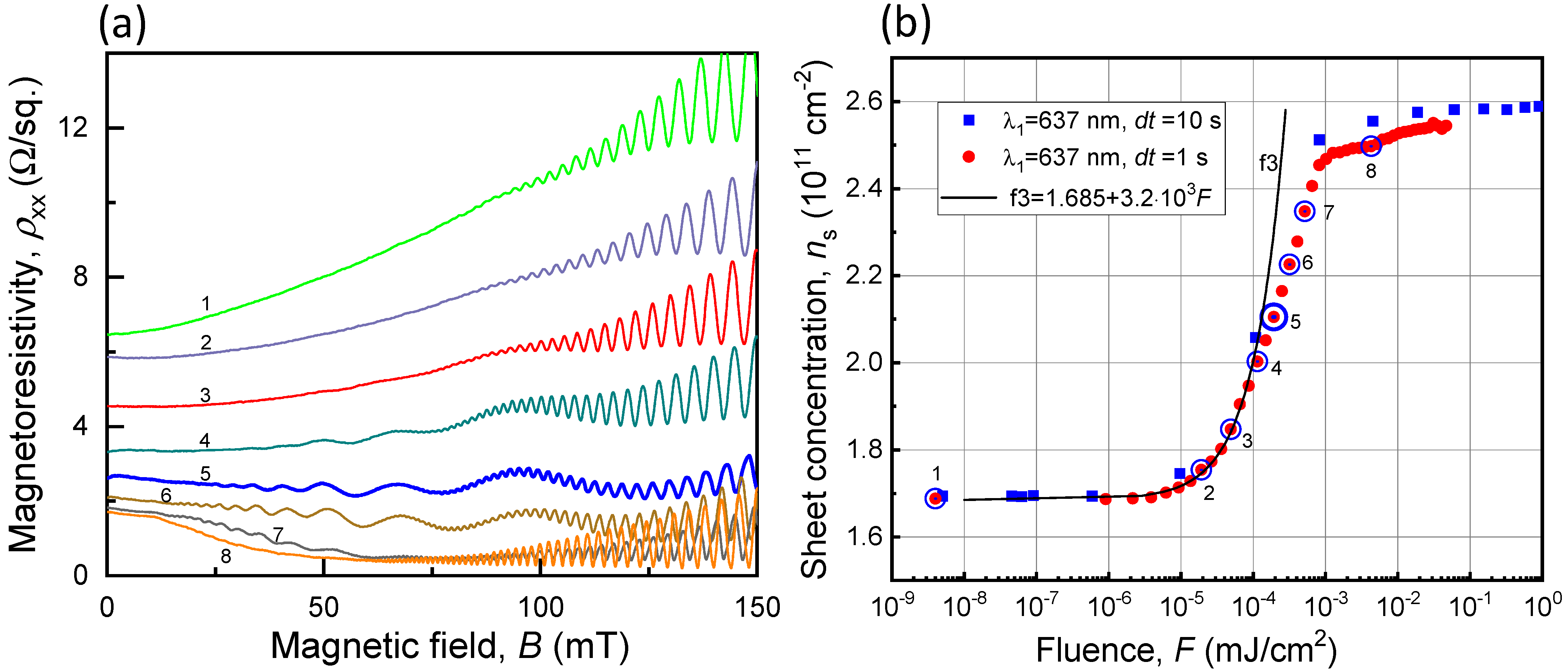
3.2. Hall Bar Illumination at = 637 nm
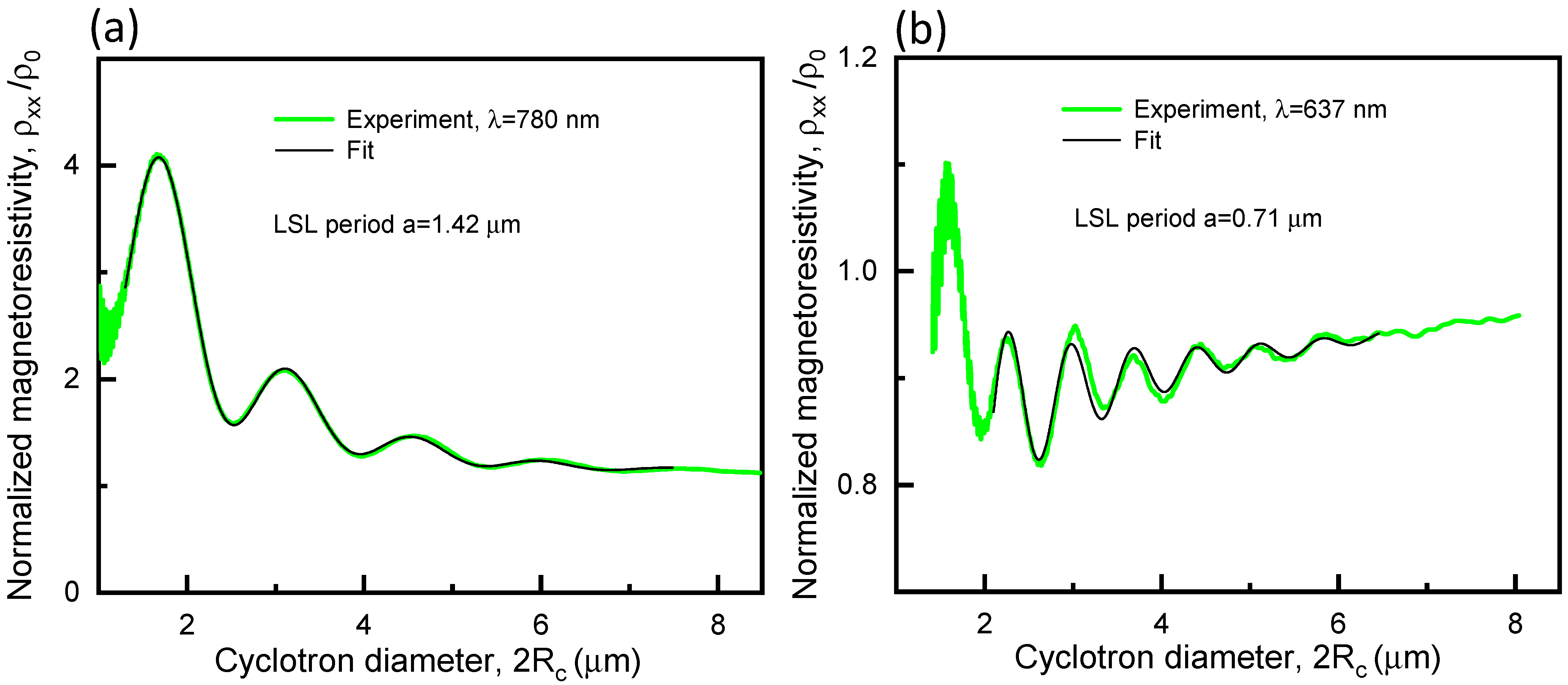
3.3. Wavelength Dependence of LSLs’ Periods
4. Discussion
Author Contributions
Funding
Data Availability Statement
Conflicts of Interest
References
- Kvon, Z.D.; Kol’tsov, B.B.; Neizvestny, I.G.; Ovsyuk, V.N. Two-dimensional hole gas in a one-dimensional superlattice. JETP Lett. 1981, 33, 571–574. [Google Scholar]
- Studenikin, S.A.; Rechkunov, S.N.; Toropov, A.I.; Koenraad, P. Quantum magnetotransport oscillations of 2DEG in a short-period InAs lateral superlattice on a vicinal (001) surface in a GaAs/AlGaAs heterostructure. Semicond. Sci. Technol. 2002, 17, 1. [Google Scholar] [CrossRef]
- Gusev, G.M.; Kvon, Z.D.; Besman, V.B.; Wilms, P.P.; Kovalenko, N.V.; Moshegov, N.G.; Toropov, A.I. Shubnikov-de-Haase oscillations of a two-dimensional electron gas in a two-dimensional periodic potential. Semicond. Phys. Technol. (Fiz.Techn. Poluprov.) 1992, 26, 539. [Google Scholar]
- Buldygin, A.F.; Magarill, L.I.; Panaev, I.A.; Studenikin, S.A.; Wilms, P.P.; Kovalenko, N.V. Investigation of dynamic conductivity of surface two-dimensional superlattice on GaAs/AlGaAs by non-contact microwave method in a magnetic field. Semicond. Phys. Technol. (Fiz.Techn. Poluprov.) 1994, 28, 1562–1568. [Google Scholar]
- Magarill, L.I.; Panaev, I.A.; Studenikin, S.A. Dynamic conductivity of a lateral-surface superlattice in a magnetic field. J. Phys. Condens. Matter 1995, 7, 1101–1110. [Google Scholar] [CrossRef]
- Skuras, E.; Long, A.R.; Larkin, I.A.; Davies, J.H.; Holland, M.C. Anisotropic piezoelectric effect in lateral surface superlattices. Appl. Phys. Lett. 1997, 70, 871–873. [Google Scholar] [CrossRef]
- Kamburov, D.; Shayegan, M.; Pfeiffer, L.N.; West, K.W.; Baldwin, K.W. Commensurability Oscillations of Hole-Flux Composite Fermions. Phys. Rev. Lett. 2012, 109, 236401. [Google Scholar] [CrossRef]
- Tanaka, K.; Falson, J.; Kozuka, Y.; Uchida, M.; Maryenko, D.; Ye, J.T.; Iwasa, Y.; Tsukazaki, A.; Smet, J.H.; Kawasaki, M. Ballistic transport in periodically modulated MgZnO/ZnO two-dimensional electron systems. Appl. Phys. Lett. 2019, 115, 153101. [Google Scholar] [CrossRef]
- Nádvorník, L.; Orlita, M.; Goncharuk, N.A.; Smrčka, L.; Novák, V.; Jurka, V.; Hruška, K.; Výborný, Z.; Wasilewski, Z.R.; Potemski, M.; et al. From laterally modulated two-dimensional electron gas towards artificial graphene. New J. Phys. 2012, 14, 053002. [Google Scholar] [CrossRef]
- Dean, C.R.; Wang, L.; Maher, P.; Forsythe, C.; Ghahari, F.; Gao, Y.; Katoch, J.; Ishigami, M.; Moon, P.; Koshino, M.; et al. Hofstadter’s butterfly and the fractal quantum Hall effect in moire superlattices. Nature 2013, 497, 598–602. [Google Scholar] [CrossRef]
- Shi, B.; Qi, P.; Jiang, M.; Dai, Y.; Lin, F.; Zhang, H.; Fang, Z. Exotic physical properties of 2D materials modulated by moiré superlattices. Mater. Adv. 2021, 2, 5542–5559. [Google Scholar] [CrossRef]
- Weiss, D.; Klitzing, K.V.; Ploog, K.; Weimann, G. Magnetoresistance Oscillations in a Two-Dimensional Electron Gas Induced by a Submicrometer Periodic Potential. Europhys. Lett. (EPL) 1989, 8, 179–184. [Google Scholar] [CrossRef]
- Gerhardts, R.R.; Weiss, D.; Klitzing, K.V. Novel magnetoresistance oscillations in a periodically modulated two-dimensional electron gas. Phys. Rev. Lett. 1989, 62, 1173–1176. [Google Scholar] [CrossRef] [PubMed]
- Weiss, D. Lateral superlattices: Magnetoresistance, hall effect and commensurate orbits. In Festkörperprobleme 31: Plenary Lectures of the Divisions Semiconductor Physics Thin Films Dynamics and Statistical Physics Magnetism Metal Physics Surface Physics Low Temperature Physics of the German Physical Society (DPG), Münster, April 8 to 12, 1991; Rössler, U., Ed.; Springer: Berlin/Heidelberg, Germany, 1991. [Google Scholar]
- Jobst, S.; Zwerschke, S.; Smet, J.H.; Gerhardts, R.R.; Weiss, D.; von Klitzing, K.; Umansky, V. Composite fermions in a weakly density modulated 2DEG: Direct evidence of a periodic magnetic field around ν = 12. Phys. E Low-Dimens. Syst. Nanostructures 2000, 6, 87–90. [Google Scholar] [CrossRef]
- Hnatovsky, C.; Zudov, M.A.; Austing, G.D.; Bogan, A.; Mihailov, S.J.; Hilke, M.; West, K.W.; Pfeiffer, L.N.; Studenikin, S.A. Inscription of lateral superlattices in semiconductors using structured light. J. Appl. Phys. 2022, 132, 044301. [Google Scholar] [CrossRef]
- Chung, Y.J.; Gupta, A.; Baldwin, K.W.; West, K.W.; Shayegan, M.; Pfeiffer, L.N. Understanding limits to mobility in ultrahigh-mobility GaAs two-dimensional electron systems: 100 million cm2/Vs and beyond. Phys. Rev. B 2022, 106, 075134. [Google Scholar] [CrossRef]
- Hill, K.O.; Malo, B.; Bilodeau, F.; Johnson, D.C.; Albert, J. Bragg gratings fabricated in monomode photosensitive optical fiber by UV exposure through a phase mask. Appl. Phys. Lett. 1993, 62, 1035–1037. [Google Scholar] [CrossRef]
- Mihailov, S.J.; Smelser, C.W.; Lu, P.; Walker, R.B.; Grobnic, D.; Ding, H.; Henderson, G.; Unruh, J. Fiber Bragg gratings made with a phase mask and 800-nm femtosecond radiation. Opt. Lett. 2003, 28, 995–997. [Google Scholar] [CrossRef]
- Kashyap, R. Fiber Bragg Gratings; Elsevier Inc.: Amsterdam, The Netherlands, 2009; p. 632. [Google Scholar]
- Born, M.; Wolf, E. Principles of optics: Electromagnetic Theory of Propagation, Interference and Diffraction of Light (7th Expanded Ed.); Cambridge University Press: Cambridge, UK, 1999. [Google Scholar]
- Kim, M.-S.; Scharf, T.; Menzel, C.; Rockstuhl, C.; Herzig, H.P. Talbot images of wavelength-scale amplitude gratings. Opt. Express 2012, 20, 4903–4920. [Google Scholar] [CrossRef]
- Mills, J.D.; Hillman, C.W.J.; Blott, B.H.; Brocklesby, W.S. Imaging of free-space interference patterns used to manufacture fiber Bragg gratings. Appl. Opt. 2000, 39, 6128–6135. [Google Scholar] [CrossRef]
- Hnatovsky, C.; Grobnic, D.; Mihailov, S.J. High-temperature stable phase-shifted fiber Bragg gratings inscribed using infrared femtosecond pulses and a phase mask. Opt. Express 2018, 26, 23550–23564. [Google Scholar] [CrossRef] [PubMed]
- Lang, D.V.; Logan, R.A.; Jaros, M. Trapping characteristics and a donor-complex (DX) model for the persistent-photoconductivity trapping center in Te-doped AlxGa1−xAs. Phys. Rev. B 1979, 19, 1015–1030. [Google Scholar] [CrossRef]
- Mooney, P.M. Deep donor levels (DX centers) in III–V semiconductors. J. Appl. Phys. 1990, 67, R1–R26. [Google Scholar] [CrossRef]
- Monemar, B.; Shih, K.K.; Pettit, G.D. Some optical properties of the AlxGa1−xAs alloys system. J. Appl. Phys. 1976, 47, 2604–2613. [Google Scholar] [CrossRef]
- Liu, T.; Xiang, D.; Zheng, Y.; Wang, Y.; Wang, X.; Wang, L.; He, J.; Liu, L.; Chen, W. Nonvolatile and Programmable Photodoping in MoTe2 for Photoresist-Free Complementary Electronic Devices. Adv. Mater. 2018, 30, 1804470. [Google Scholar] [CrossRef] [PubMed]
- Murakami, Y.; Takayoshi, S.; Kaneko, T.; Läuchli, A.M.; Werner, P. Spin, Charge, and eta-Spin Separation in One-Dimensional Photodoped Mott Insulators. Phys. Rev. Lett. 2023, 130, 106501. [Google Scholar] [CrossRef] [PubMed]
- Schaefer, S.T.; Gao, S.; Webster, P.T.; Kosireddy, R.R.; Johnson, S.R. Absorption edge characteristics of GaAs, GaSb, InAs, and InSb. J. Appl. Phys. 2020, 127, 165705. [Google Scholar] [CrossRef]
- Fu, X.; Riedl, A.; Borisov, M.; Zudov, M.A.; Watson, J.D.; Gardner, G.; Manfra, M.J.; Baldwin, K.W.; Pfeiffer, L.N.; West, K.W. Effect of illumination on quantum lifetime in GaAs quantum wells. Phys. Rev. B 2018, 98, 195403. [Google Scholar] [CrossRef]
- Shetty, A.; Sfigakis, F.; Mak, W.Y.; Das Gupta, K.; Buonacorsi, B.; Tam, M.C.; Kim, H.S.; Farrer, I.; Croxall, A.F.; Beere, H.E.; et al. Effects of biased and unbiased illuminations on two-dimensional electron gases in dopant-free GaAs/AlGaAs. Phys. Rev. B 2022, 105, 075302. [Google Scholar] [CrossRef]
- De Cesari, S.; Balocchi, A.; Vitiello, E.; Jahandar, P.; Grilli, E.; Amand, T.; Marie, X.; Myronov, M.; Pezzoli, F. Spin-coherent dynamics and carrier lifetime in strained GeSn semiconductors on silicon. Phys. Rev. B 2019, 99, 035202. [Google Scholar] [CrossRef]
- Assali, S.; Attiaoui, A.; Vecchio, P.D.; Mukherjee, S.; Nicolas, J.; Moutanabbir, O. A Light-Hole Germanium Quantum Well on Silicon. Adv. Mater. 2022, 34, 2201192. [Google Scholar] [CrossRef] [PubMed]
- Oiwa, A.; Fujita, T.; Kiyama, H.; Allison, G.; Ludwig, A.; Wieck, A.D.; Tarucha, S. Conversion from Single Photon to Single Electron Spin Using Electrically Controllable Quantum Dots. J. Phys. Soc. Jpn. 2016, 86, 011008. [Google Scholar] [CrossRef]
- Gaudreau, L.; Bogan, A.; Korkusinski, M.; Studenikin, S.; Austing, D.G.; Sachrajda, A.S. Entanglement distribution schemes employing coherent photon-to-spin conversion in semiconductor quantum dot circuits. Semicond. Sci. Technol. 2017, 32, 093001–093014. [Google Scholar] [CrossRef]
- Chung, Y.J.; Villegas Rosales, K.A.; Baldwin, K.W.; Madathil, P.T.; West, K.W.; Shayegan, M.; Pfeiffer, L.N. Ultra-high-quality two-dimensional electron systems. Nat. Mater. 2021, 20, 632–637. [Google Scholar] [CrossRef] [PubMed]
- Shi, Q.; Studenikin, S.A.; Zudov, M.A.; Baldwin, K.W.; Pfeiffer, L.N.; West, K.W. Microwave photoresistance in an ultra-high-quality GaAs quantum well. Phys. Rev. B 2016, 93, 121305–121310. [Google Scholar] [CrossRef]
- Myronov, M.; Kycia, J.; Waldron, P.; Jiang, W.; Barrios, P.; Bogan, A.; Coleridge, P.; Studenikin, S. Holes Outperform Electrons in Group IV Semiconductor Materials. Small Sci. 2023, 3, 2200094. [Google Scholar] [CrossRef]
- Chung, Y.J.; Wang, C.; Singh, S.K.; Gupta, A.; Baldwin, K.W.; West, K.W.; Shayegan, M.; Pfeiffer, L.N.; Winkler, R. Record-quality GaAs two-dimensional hole systems. Phys. Rev. Mater. 2022, 6, 034005. [Google Scholar] [CrossRef]


Disclaimer/Publisher’s Note: The statements, opinions and data contained in all publications are solely those of the individual author(s) and contributor(s) and not of MDPI and/or the editor(s). MDPI and/or the editor(s) disclaim responsibility for any injury to people or property resulting from any ideas, methods, instructions or products referred to in the content. |
© 2023 by the authors. Licensee MDPI, Basel, Switzerland. This article is an open access article distributed under the terms and conditions of the Creative Commons Attribution (CC BY) license (https://creativecommons.org/licenses/by/4.0/).
Share and Cite
Hnatovsky, C.; Mihailov, S.; Hilke, M.; Pfeiffer, L.; West, K.; Studenikin, S. An Optical Technique to Produce Embedded Quantum Structures in Semiconductors. Nanomaterials 2023, 13, 1622. https://doi.org/10.3390/nano13101622
Hnatovsky C, Mihailov S, Hilke M, Pfeiffer L, West K, Studenikin S. An Optical Technique to Produce Embedded Quantum Structures in Semiconductors. Nanomaterials. 2023; 13(10):1622. https://doi.org/10.3390/nano13101622
Chicago/Turabian StyleHnatovsky, Cyril, Stephen Mihailov, Michael Hilke, Loren Pfeiffer, Ken West, and Sergei Studenikin. 2023. "An Optical Technique to Produce Embedded Quantum Structures in Semiconductors" Nanomaterials 13, no. 10: 1622. https://doi.org/10.3390/nano13101622