
Uniformity of HfO2 Thin Films Prepared on Trench Structures via Plasma-Enhanced Atomic Layer Deposition

Abstract
:1. Introduction
2. Materials and Methods
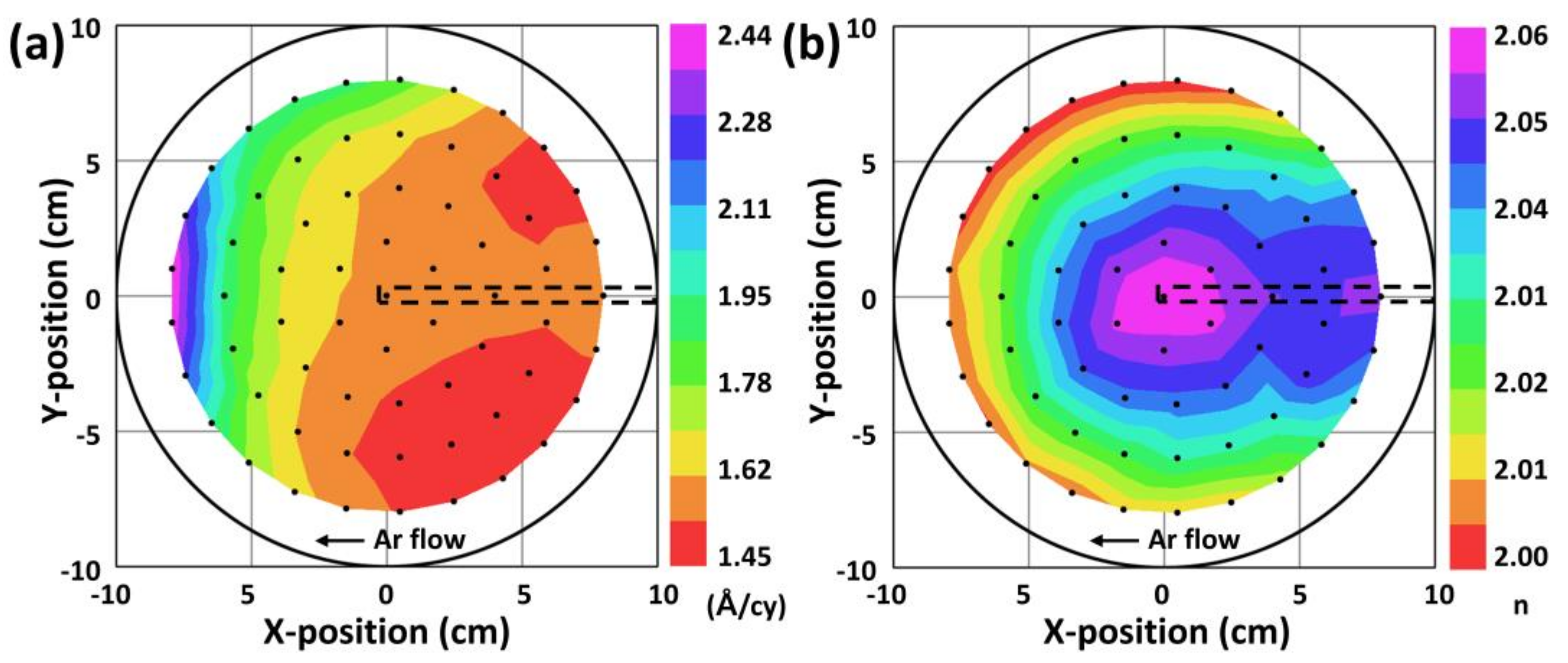
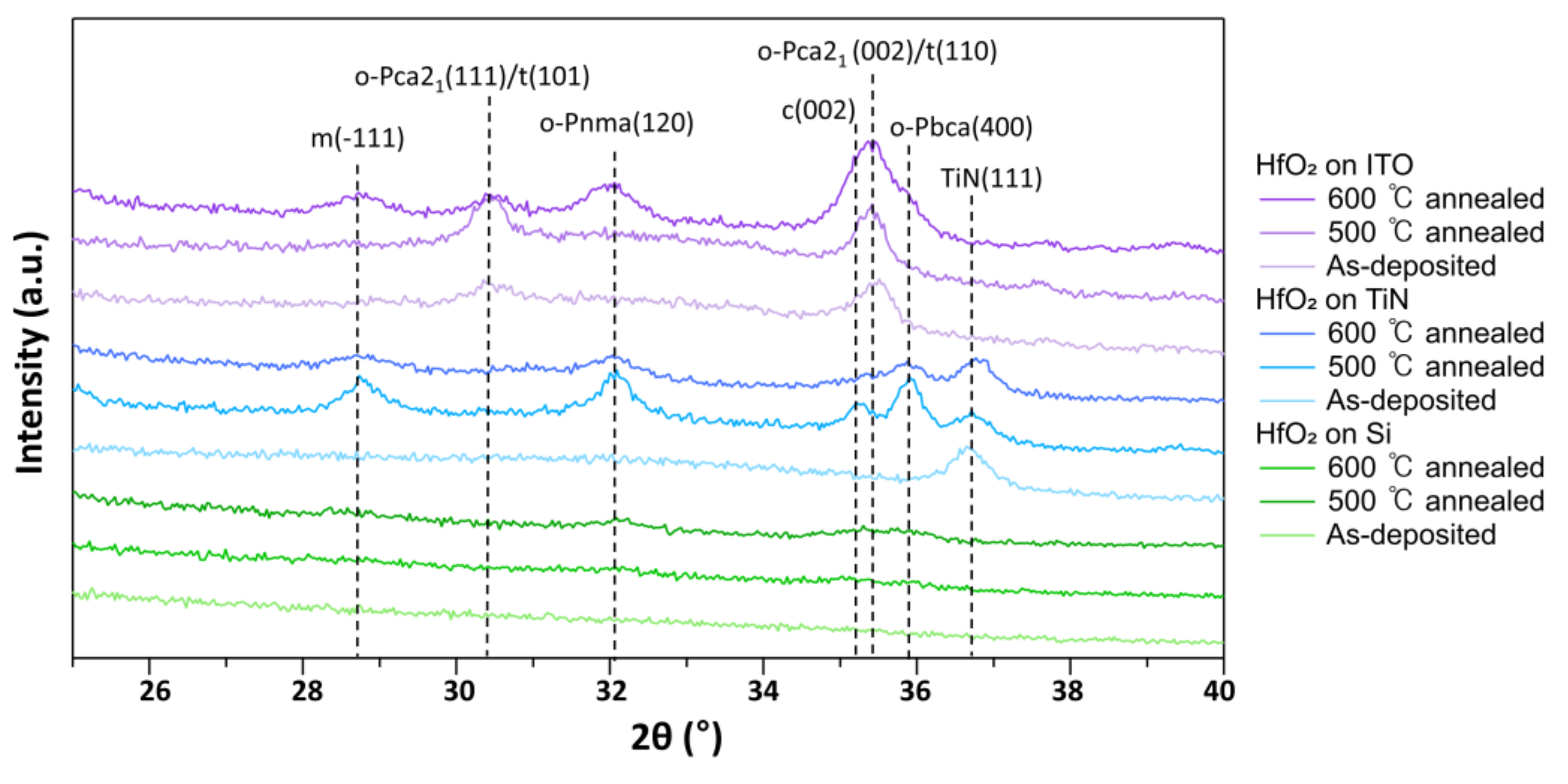
3. Results
4. Conclusions
Supplementary Materials
Author Contributions
Funding
Data Availability Statement
Conflicts of Interest
References
- Cho, Y.J.; Nguyen, N.; Richter, C.; Ehrstein, J.; Lee, B.H.; Lee, J.C. Spectroscopic ellipsometry characterization of high-k dielectric HfO2 thin films and the high-temperature annealing effects on their optical properties. Appl. Phys. Lett. 2002, 80, 1249–1251. [Google Scholar] [CrossRef] [Green Version]
- Jones, M.; Kwon, Y.; Norton, D. Dielectric constant and current transport for HfO2 thin films on ITO. Appl. Phys. A 2005, 81, 285–288. [Google Scholar] [CrossRef]
- Suzuki, K.; Kato, K. Sol–gel synthesis of high-k HfO2 thin films. J. Am. Ceram. Soc. 2009, 92, S162–S164. [Google Scholar] [CrossRef]
- Tirmali, P.; Khairnar, A.G.; Joshi, B.N.; Mahajan, A.M. Structural and electrical characteristics of RF-sputtered HfO2 high-k based MOS capacitors. Solid-State Electron. 2011, 62, 44–47. [Google Scholar] [CrossRef]
- Polakowski, P.; Müller, J. Ferroelectricity in undoped hafnium oxide. Appl. Phys. Lett. 2015, 106, 232905. [Google Scholar] [CrossRef]
- Sang, X.; Grimley, E.D.; Schenk, T.; Schroeder, U.; LeBeau, J.M. On the structural origins of ferroelectricity in HfO2 thin films. Appl. Phys. Lett. 2015, 106, 162905. [Google Scholar] [CrossRef]
- Mueller, S.; Muller, J.; Schroeder, U.; Mikolajick, T. Reliability Characteristics of Ferroelectric Si:HfO2 Thin Films for Memory Applications. IEEE Trans. Device Mater. Reliab. 2012, 13, 93–97. [Google Scholar] [CrossRef]
- Choi, S.-N.; Moon, S.-E.; Yoon, S.-M. Film thickness-dependent ferroelectric polarization switching dynamics of undoped HfO2 thin films prepared by atomic layer deposition. Ceram. Int. 2019, 45, 22642–22648. [Google Scholar] [CrossRef]
- Hackley, J.C.; Gougousi, T. Properties of atomic layer deposited HfO2 thin films. Thin Solid Films 2009, 517, 6576–6583. [Google Scholar] [CrossRef]
- Hur, J.; Tasneem, N.; Choe, G.; Wang, P.; Wang, Z.; Khan, A.I.; Yu, S. Direct comparison of ferroelectric properties in Hf0.5Zr0.5O2 between thermal and plasma-enhanced atomic layer deposition. Nanotechnology 2020, 31, 505707. [Google Scholar] [CrossRef]
- Nigro, R.L.; Schilirò, E.; Mannino, G.; Di Franco, S.; Roccaforte, F. Comparison between thermal and plasma enhanced atomic layer deposition processes for the growth of HfO2 dielectric layers. J. Cryst. Growth 2020, 539, 125624. [Google Scholar] [CrossRef]
- Kim, K.; Park, M.; Kim, H.; Kim, Y.; Moon, T.; Lee, Y.; Hyun, S.; Gwon, T.; Hwang, C. Ferroelectricity in undoped-HfO2 thin films induced by deposition temperature control during atomic layer deposition. J. Mater. Chem. C 2016, 4, 6864–6872. [Google Scholar] [CrossRef]
- Lomenzo, P.D.; Takmeel, Q.; Moghaddam, S.; Nishida, T. Annealing behavior of ferroelectric Si-doped HfO2 thin films. Thin Solid Films 2016, 615, 139–144. [Google Scholar] [CrossRef]
- Park, M.H.; Schenk, T.; Schroeder, U. Dopants in atomic layer deposited HfO2 thin films. In Ferroelectricity in Doped Hafnium Oxide: Materials, Properties and Devices; Uwe, S., Cheol Seong, H., Hiroshi, F., Eds.; Elsevier: Amsterdam, The Netherlands, 2019; pp. 49–74. [Google Scholar] [CrossRef]
- Cortez-Valadez, M.; Fierro, C.; Farias-Mancilla, J.; Vargas-Ortiz, A.; Flores-Acosta, M.; Ramírez-Bon, R.; Enriquez-Carrejo, J.; Soubervielle-Montalvo, C.; Mani-Gonzalez, P. Comparison of HfCl4, HfI4, TEMA-Hf, and TDMA-Hf as precursors in early growing stages of HfO2 films deposited by ALD: A DFT study. Chem. Phys. 2016, 472, 81–88. [Google Scholar] [CrossRef]
- Huan, T.D.; Sharma, V.; Rossetti, G.A., Jr.; Ramprasad, R. Pathways towards ferroelectricity in hafnia. Phys. Rev. B 2014, 90, 064111. [Google Scholar] [CrossRef] [Green Version]
- Oh, I.-K.; Park, B.-E.; Seo, S.; Yeo, B.C.; Tanskanen, J.; Kim, W.-H.; Kim, H. Comparative study of the growth characteristics and electrical properties of atomic-layer-deposited HfO2 films obtained from metal halide and amide precursors. J. Mater. Chem. C 2018, 6, 7367–7376. [Google Scholar] [CrossRef]
- Kakanakova-Georgieva, A.; Giannazzo, F.; Nicotra, G.; Cora, I.; Gueorguiev, G.K.; Persson, P.O.; Pécz, B. Material proposal for 2D indium oxide. Appl. Surf. Sci. 2021, 548, 149275. [Google Scholar] [CrossRef]
- Dos Santos, R.B.; Rivelino, R.; Gueorguiev, G.K.; Kakanakova-Georgieva, A. Exploring 2D structures of indium oxide of different stoichiometry. CrystEngComm 2021, 23, 6661–6667. [Google Scholar] [CrossRef]
- Pyeon, J.J.; Kim, S.H.; Jeong, D.S.; Baek, S.-H.; Kang, C.-Y.; Kim, J.-S.; Kim, S.K. Wafer-scale growth of MoS2 thin films by atomic layer deposition. Nanoscale 2016, 8, 10792–10798. [Google Scholar] [CrossRef]
- Zhang, H.-T.; Zhang, L.; Mukherjee, D.; Zheng, Y.-X.; Haislmaier, R.C.; Alem, N.; Engel-Herbert, R. Wafer-scale growth of VO2 thin films using a combinatorial approach. Nat. Commun. 2015, 6, 8475. [Google Scholar] [CrossRef] [Green Version]
- Kim, H.-S.; Patel, M.; Kim, J.; Jeong, M.S. Growth of wafer-scale standing layers of WS2 for self-biased high-speed UV–visible–NIR optoelectronic devices. ACS Appl. Mater. Interfaces 2018, 10, 3964–3974. [Google Scholar] [CrossRef] [PubMed]
- Patel, M.; Kim, H.-S.; Kim, J. Wafer-scale production of vertical SnS multilayers for high-performing photoelectric devices. Nanoscale 2017, 9, 15804–15812. [Google Scholar] [CrossRef] [PubMed]
- Patel, M.; Nguyen, T.T.; Kumar, M.; Ban, D.-K.; Won, D.; Zhao, M.; Kim, J.; Kim, Y.K.; Yang, H.; Wong, C.-P. 2D layer-embedded transparent photovoltaics. Nano Energy 2020, 68, 104328. [Google Scholar] [CrossRef]
- Lapteva, M.; Beladiya, V.; Riese, S.; Hanke, P.; Otto, F.; Fritz, T.; Schmitt, P.; Stenzel, O.; Tünnermann, A.; Szeghalmi, A. Influence of temperature and plasma parameters on the properties of PEALD HfO2. Opt. Mater. Express 2021, 11, 1918–1942. [Google Scholar] [CrossRef]
- Schroeder, U.; Park, M.H.; Mikolajick, T.; Hwang, C.S. The fundamentals and applications of ferroelectric HfO2. Nat. Rev. Mater. 2022, 7, 653–669. [Google Scholar] [CrossRef]
- Park, M.H.; Lee, Y.H.; Mikolajick, T.; Schroeder, U.; Hwang, C.S. Review and perspective on ferroelectric HfO2-based thin films for memory applications. Mrs Commun. 2018, 8, 795–808. [Google Scholar] [CrossRef] [Green Version]
- Choi, S.-N.; Moon, S.-E.; Yoon, S.-M. Impact of oxide gate electrode for ferroelectric field-effect transistors with metal-ferroelectric-metal-insulator-semiconductor gate stack using undoped HfO2 thin films prepared by atomic layer deposition. Nanotechnology 2020, 32, 085709. [Google Scholar] [CrossRef]
- Zhang, W.; Zhou, D.; Sun, N.; Wang, J.; Li, S. Effect of Bias Voltage on Substrate for the Structure and Electrical Properties of Y: HfO2 Thin Films Deposited by Reactive Magnetron Co-Sputtering. Adv. Electron. Mater. 2021, 7, 2100488. [Google Scholar] [CrossRef]
- Cremers, V.; Puurunen, R.L.; Dendooven, J. Conformality in atomic layer deposition: Current status overview of analysis and modelling. Appl. Phys. Rev. 2019, 6, 021302. [Google Scholar] [CrossRef]
- Melo, L.; Burton, G.; Kubik, P.; Wild, P. Long period gratings coated with hafnium oxide by plasma-enhanced atomic layer deposition for refractive index measurements. Opt. Express 2016, 24, 7654–7669. [Google Scholar] [CrossRef]
- Provine, J.; Schindler, P.; Torgersen, J.; Kim, H.J.; Karnthaler, H.-P.; Prinz, F.B. Atomic layer deposition by reaction of molecular oxygen with tetrakisdimethylamido-metal precursors. J. Vac. Sci. Technol. A Vac. Surf. Film. 2016, 34, 01A138. [Google Scholar] [CrossRef] [Green Version]
- Alam, A.; Howlader, M.; Deen, M. The effects of oxygen plasma and humidity on surface roughness, water contact angle and hardness of silicon, silicon dioxide and glass. J. Micromech. Microeng. 2014, 24, 035010. [Google Scholar] [CrossRef] [Green Version]
- Heo, J.H.; Ryu, H.; Lee, W.-J. Effect of O2 plasma pretreatment on structural and optical properties of ZnO films on PES substrate by atomic layer deposition. J. Ind. Eng. Chem. 2013, 19, 1638–1641. [Google Scholar] [CrossRef]
- Zhu, Z.; Sippola, P.; Lipsanen, H.; Savin, H.; Merdes, S. Influence of plasma parameters on the properties of ultrathin Al2O3 films prepared by plasma enhanced atomic layer deposition below 100 °C for moisture barrier applications. Jpn. J. Appl. Phys. 2018, 57, 125502. [Google Scholar] [CrossRef] [Green Version]
- Afshar, A. Materials Characterization and Growth Mechanisms of ZnO, ZrO2, and HfO2 Deposited by Atomic Layer Deposition. Ph.D. Thesis, University of Alberta, Alberta, AB, Canada, 2014. [Google Scholar] [CrossRef]
- Blaschke, D.; Munnik, F.; Grenzer, J.; Rebohle, L.; Schmidt, H.; Zahn, P.; Gemming, S. A correlation study of layer growth rate, thickness uniformity, stoichiometry, and hydrogen impurity level in HfO2 thin films grown by ALD between 100 °C and 350 °C. Appl. Surf. Sci. 2020, 506, 144188. [Google Scholar] [CrossRef]
- Kolanek, K.; Tallarida, M.; Michling, M.; Schmeisser, D. In situ study of the atomic layer deposition of HfO2 on Si. J. Vac. Sci. Technol. A Vac. Surf. Film. 2012, 30, 01A143. [Google Scholar] [CrossRef]
- Singh, R.; Panigrahi, J.; Singh, P. Plasma assisted atomic layer deposited hafnium oxide films for silicon surface passivation. RSC Adv. 2016, 6, 97720–97727. [Google Scholar] [CrossRef]
- Li, S.; Zhang, Y.; Yang, D.; Yang, W.; Chen, X.; Zhao, H.; Hou, J.; Yang, P. Structure and optical properties of HfO2 films on Si (100) substrates prepared by ALD at different temperatures. Phys. B Condens. Matter 2020, 584, 412065. [Google Scholar] [CrossRef]
- Foroughi Abari, A. Atomic Layer Deposition of Metal Oxide Thin Films on Metallic Substrates. Ph.D. Thesis, University of Alberta, Alberta, AB, Canada, 2012. [Google Scholar] [CrossRef]
- Kukli, K.; Pilvi, T.; Ritala, M.; Sajavaara, T.; Lu, J.; Leskelä, M. Atomic layer deposition of hafnium dioxide thin films from hafnium tetrakis (dimethylamide) and water. Thin Solid Films 2005, 491, 328–338. [Google Scholar] [CrossRef]
- Martínez-Puente, M.; Horley, P.; Aguirre-Tostado, F.; López-Medina, J.; Borbón-Nuñez, H.; Tiznado, H.; Susarrey-Arce, A.; Martínez-Guerra, E. ALD and PEALD deposition of HfO2 and its effects on the nature of oxygen vacancies. Mater. Sci. Eng. B 2022, 285, 115964. [Google Scholar] [CrossRef]
- Triyoso, D.; Liu, R.; Roan, D.; Ramon, M.; Edwards, N.; Gregory, R.; Werho, D.; Kulik, J.; Tam, G.; Irwin, E. Impact of deposition and annealing temperature on material and electrical characteristics of ALD HfO2. J. Electrochem. Soc. 2004, 151, F220. [Google Scholar] [CrossRef]
- Zanders, D.; Ciftyurek, E.; Subaşı, E.; Huster, N.; Bock, C.; Kostka, A.; Rogalla, D.; Schierbaum, K.; Devi, A. PEALD of HfO2 thin films: Precursor tuning and a new near-ambient-pressure XPS approach to in situ examination of thin-film surfaces exposed to reactive gases. ACS Appl. Mater. Interfaces 2019, 11, 28407–28422. [Google Scholar] [CrossRef] [PubMed]
- Miakonkikh, A.; Lomov, A.; Rogozhin, A.; Rudenko, K.; Lukichev, V.; Kiselev, D.; Tikhonenlo, F.; Antonov, V.; Popov, V. Phase transformation in ALD hafnia based layers for silicon-on-ferroelectric devices. In Proceedings of the 2020 Joint International EUROSOI Workshop and International Conference on Ultimate Integration on Silicon (EUROSOI-ULIS), Caen, France, 1–30 September 2020; pp. 1–4. [Google Scholar]
- Cho, M.-H.; Roh, Y.; Whang, C.; Jeong, K.; Nahm, S.; Ko, D.-H.; Lee, J.H.; Lee, N.; Fujihara, K. Thermal stability and structural characteristics of HfO2 films on Si (100) grown by atomic-layer deposition. Appl. Phys. Lett. 2002, 81, 472–474. [Google Scholar] [CrossRef]
- Kim, S.; Kim, J.; Choi, J.; Kang, H.; Jeon, H.; Bae, C. Characteristics of HfO2 thin films deposited by plasma-enhanced atomic layer deposition using O2 plasma and N2O plasma. J. Vac. Sci. Technol. B Microelectron. Nanometer Struct. Process. Meas. Phenom. 2006, 24, 1088–1093. [Google Scholar] [CrossRef]
- Nie, X.; Ma, D.; Ma, F.; Xu, K. Thermal stability, structural and electrical characteristics of the modulated HfO2/Al2O3 films fabricated by atomic layer deposition. J. Mater. Sci. 2017, 52, 11524–11536. [Google Scholar] [CrossRef]
- Wan, J.; Chen, X.; Ji, L.; Tu, Z.; Wu, H.; Liu, C. Ferroelectricity of Hf0.5Zr0.5O2 Thin Films Free from the Influence of Electrodes by Using Al2O3 Capping Layers. IEEE Trans. Electron Devices 2022, 69, 1805–1810. [Google Scholar] [CrossRef]


| Ion Density (/cm3) | Ion Flux (mA/cm2) | Electron Temperature (eV) | |
|---|---|---|---|
| O2 flow rate 10 sccm, O2 plasma power 20 W | 3.28 × 10⁸ | 0.03749 | 2.3780 |
| O2 flow rate 10 sccm, O2 plasma power 300 W | 8.03 × 10⁹ | 0.40201 | 3.0978 |
| O2 flow rate 50 sccm, O2 plasma power 20 W | 1.47 × 10⁸ | 0.02445 | 2.4841 |
| O2 flow rate 50 sccm, O2 plasma power 20 W | 4.28 × 10⁹ | 0.25453 | 3.1347 |
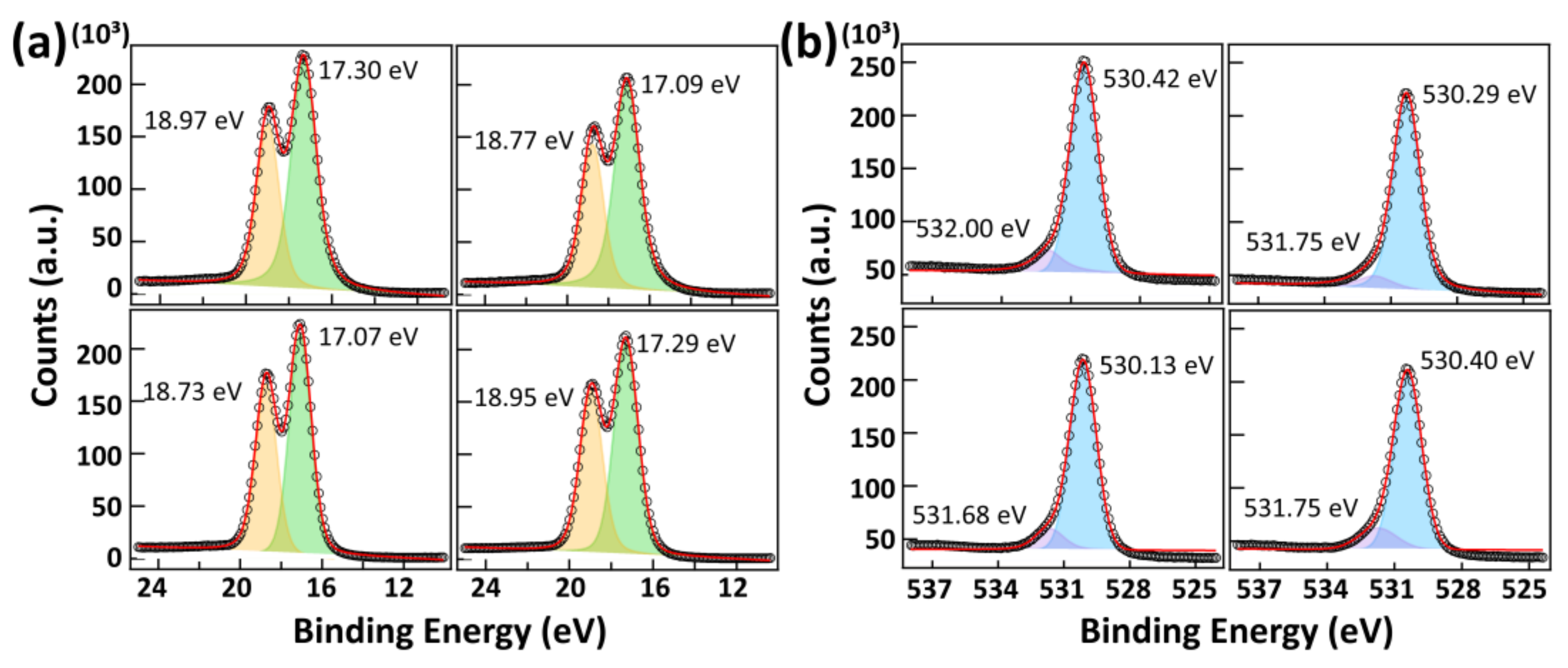
| Conditions | Atomic Concentrations (at.%) | Atomic Ratio | |||
|---|---|---|---|---|---|
| C 1s | N 1s | O 1s | Hf 4f | Hf:O | |
| (a) 10 sccm and 20 W | 2.53 | 4.86 | 65.53 | 27.08 | 1:2.42 |
| (b) 10 sccm and 300 W | 2.31 | 4.64 | 65.90 | 27.15 | 1:2.43 |
| (c) 50 sccm and 20 W | 4.25 | 5.75 | 63.38 | 26.62 | 1:2.38 |
| (d) 50 sccm and 300 W | 4.12 | 5.66 | 63.22 | 26.99 | 1:2.34 |
Disclaimer/Publisher’s Note: The statements, opinions and data contained in all publications are solely those of the individual author(s) and contributor(s) and not of MDPI and/or the editor(s). MDPI and/or the editor(s) disclaim responsibility for any injury to people or property resulting from any ideas, methods, instructions or products referred to in the content. |
© 2022 by the authors. Licensee MDPI, Basel, Switzerland. This article is an open access article distributed under the terms and conditions of the Creative Commons Attribution (CC BY) license (https://creativecommons.org/licenses/by/4.0/).
Share and Cite
Choi, B.; Kim, H.-U.; Jeon, N. Uniformity of HfO2 Thin Films Prepared on Trench Structures via Plasma-Enhanced Atomic Layer Deposition. Nanomaterials 2023, 13, 161. https://doi.org/10.3390/nano13010161
Choi B, Kim H-U, Jeon N. Uniformity of HfO2 Thin Films Prepared on Trench Structures via Plasma-Enhanced Atomic Layer Deposition. Nanomaterials. 2023; 13(1):161. https://doi.org/10.3390/nano13010161
Chicago/Turabian StyleChoi, Boyun, Hyeong-U Kim, and Nari Jeon. 2023. "Uniformity of HfO2 Thin Films Prepared on Trench Structures via Plasma-Enhanced Atomic Layer Deposition" Nanomaterials 13, no. 1: 161. https://doi.org/10.3390/nano13010161