
Nanostripe-Confined Catalyst Formation for Uniform Growth of Ultrathin Silicon Nanowires


Abstract
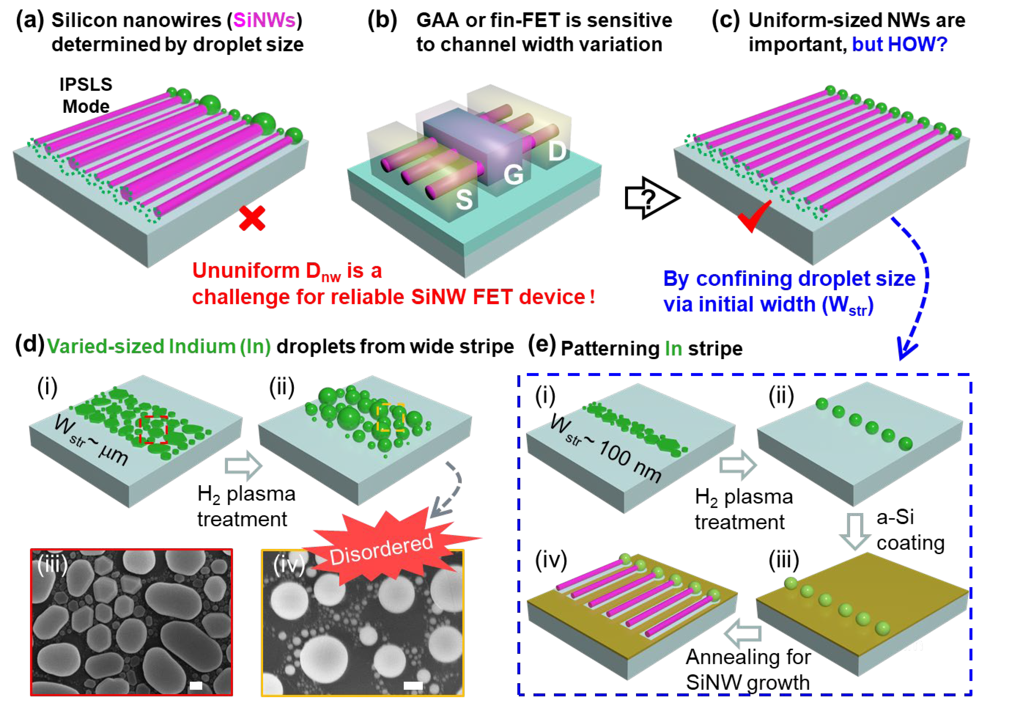
:1. Introduction
2. Materials and Methods
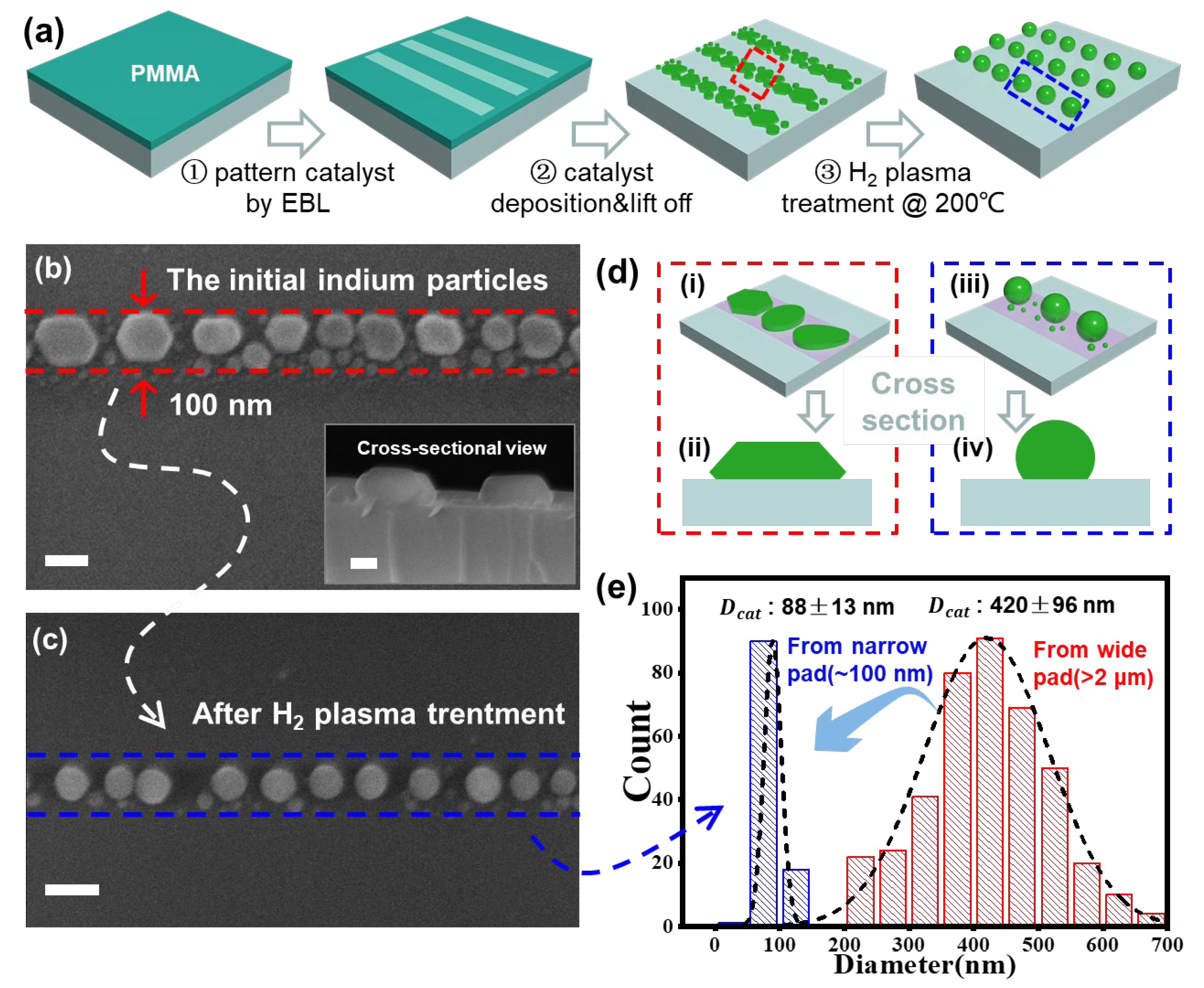
2.1. Preparation of Catalyst Nanostripes
2.2. Growth of Ultrathin SiNW Array
3. Results and Discussion
3.1. Formation of Uniform In Droplets from Narrow In Stripes
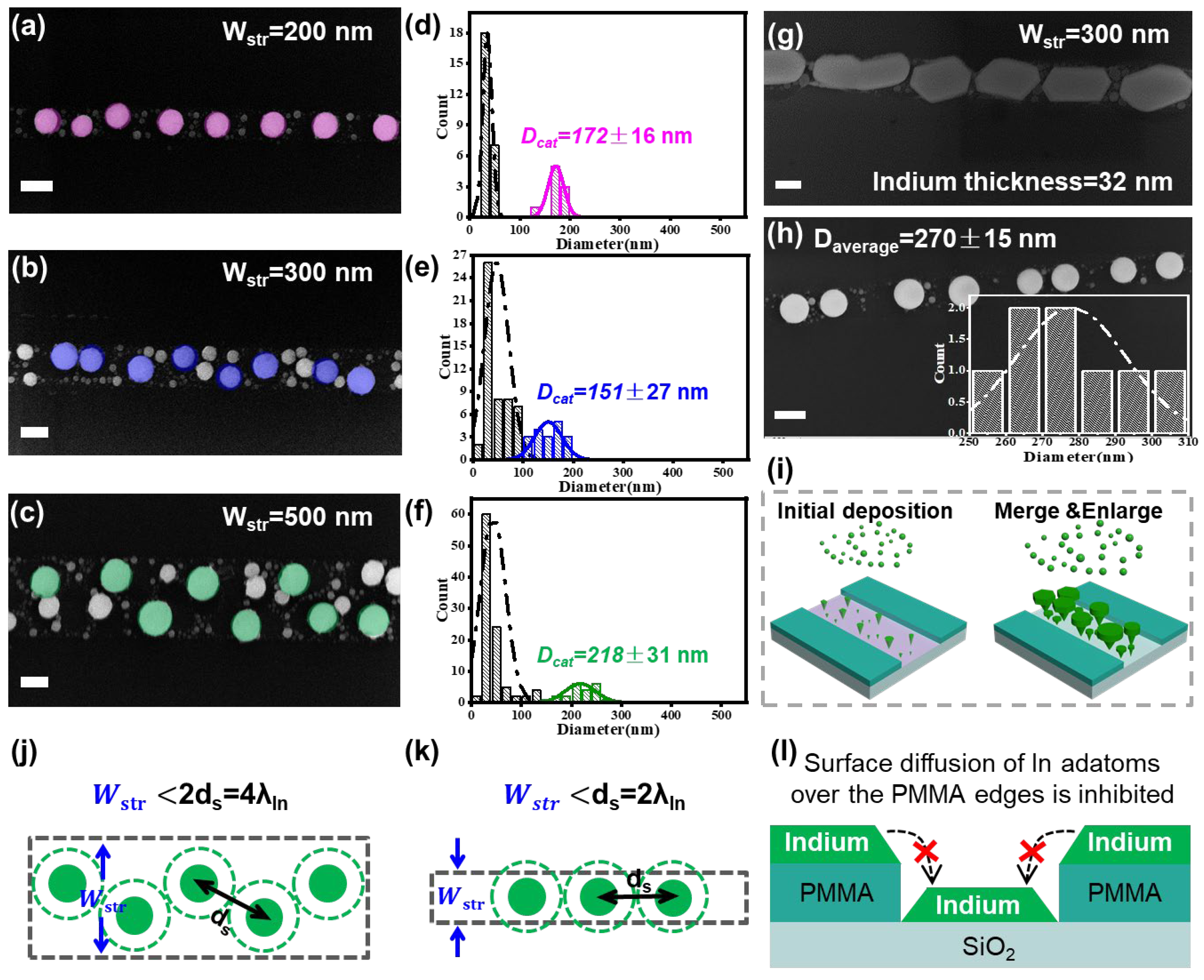
3.2. In Droplet Formation on Nanostripes of Different Widths
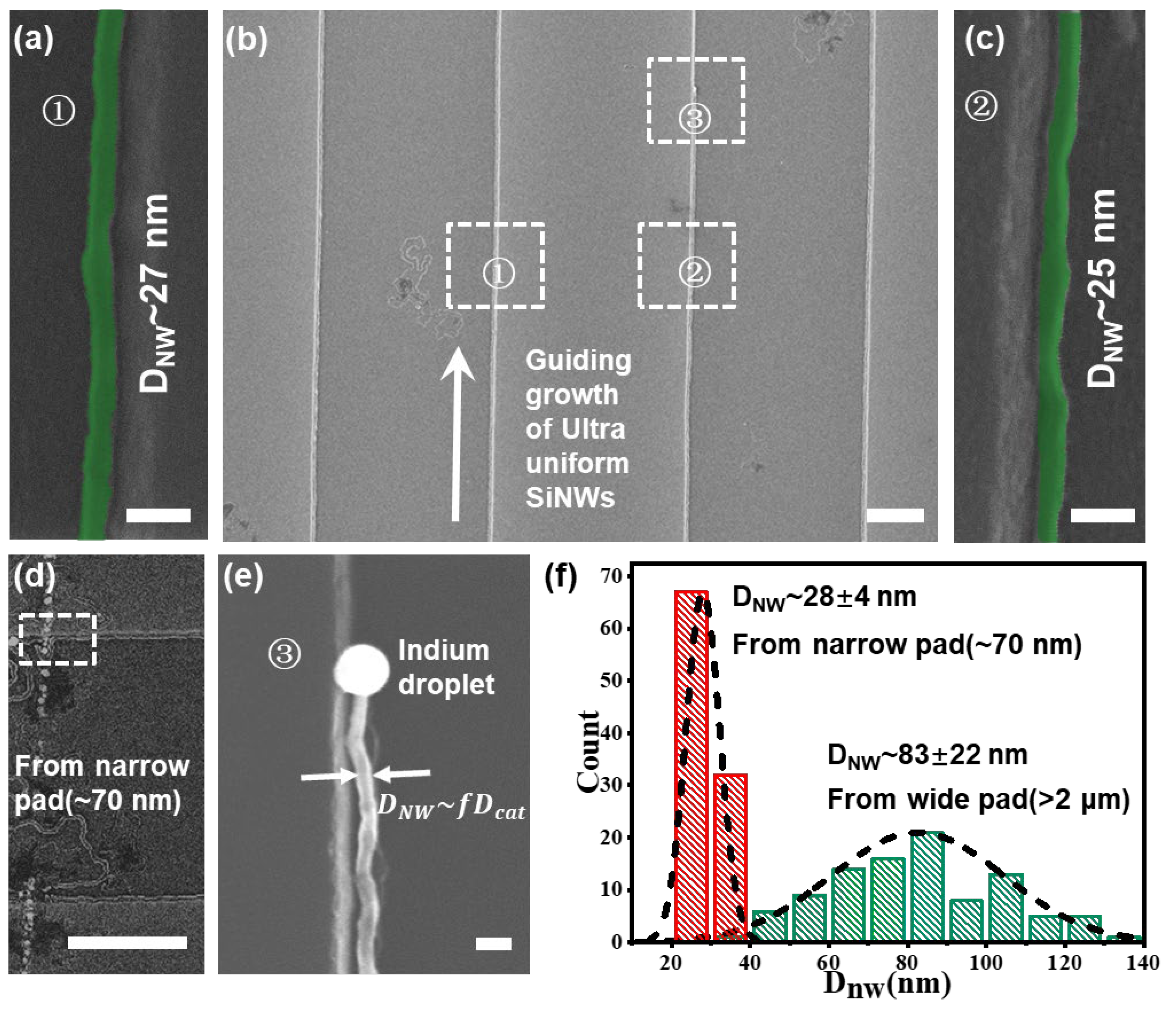
3.3. Growth of Ultrathin SiNWs Led by the Uniform In Droplets
4. Conclusions
Supplementary Materials
Author Contributions
Funding
Data Availability Statement
Conflicts of Interest
Abbreviations
References
- Cui, Y.; Zhong, Z.; Wang, D.; Wang, W.U.; Lieber, C. High performance silicon nanowire field effect transistors. Nano Lett. 2003, 3, 149–152. [Google Scholar] [CrossRef]
- Goldberger, J.; Hochbaum, A.I.; Fan, R.; Yang, P. Silicon Vertically Integrated Nanowire Field Effect Transistors. Nano Let. 2006, 6, 973–977. [Google Scholar] [CrossRef] [Green Version]
- Song, X.; Zhang, T.; Wu, L.; Hu, R.; Qian, W.; Liu, Z.; Wang, J.; Shi, Y.; Xu, J.; Chen, K.; et al. Highly Stretchable High-Performance Silicon Nanowire Field Effect Transistors Integrated on Elastomer Substrates. Adv. Sci. 2022, 9, e2105623. [Google Scholar] [CrossRef] [PubMed]
- McAlpine, M.C.; Friedman, R.S.; Jin, S.; Lin, K.-h.; Wang, W.U.; Lieber, C.M. High-performance nanowire electronics and photonics on glass and plastic substrates. Nano Lett. 2003, 3, 1531–1535. [Google Scholar] [CrossRef]
- Yan, H.; Choe, H.S.; Nam, S.; Hu, Y.; Das, S.; Klemic, J.F.; Ellenbogen, J.C.; Lieber, C.M. Programmable nanowire circuits for nanoprocessors. Nature 2011, 470, 240–244. [Google Scholar] [CrossRef]
- Lee, M.; Jeon, Y.; Moon, T.; Kim, S. Top-Down Fabrication of Fully CMOS-Compatible Silicon Nanowire Arrays and Their Integration into CMOS Inverters on Plastic. ACS Nano 2011, 5, 2629–2636. [Google Scholar] [CrossRef]
- Hsu, J.F.; Huang, B.R.; Huang, C.S.; Chen, H.L. Silicon nanowires as pH sensor. Jpn. J. Appl. Phys. 2005, 44, 2626–2629. [Google Scholar] [CrossRef] [Green Version]
- Lu, Y.; Peng, S.; Luo, D.; Lal, A. Low-concentration mechanical biosensor based on a photonic crystal nanowire array. Nat. Commun. 2011, 2, 578. [Google Scholar] [CrossRef] [Green Version]
- Tian, B.; Cohen-Karni, T.; Qing, Q.; Duan, X.; Xie, P.; Lieber, C.M. Three-dimensional, flexible nanoscale field-effect transistors as localized bioprobes. Science 2010, 329, 830–834. [Google Scholar] [CrossRef] [Green Version]
- Huang, S.; Zhang, B.; Lin, Y.; Lee, C.-S.; Zhang, X.J. Compact biomimetic hair sensors based on single silicon nanowires for ultrafast and highly-sensitive airflow detection. Nano Lett. 2021, 21, 4684–4691. [Google Scholar] [CrossRef]
- Wagner, R.S.; Ellis, W.C. Vapor-Liquid-Solid Mechanism of Single Crystal Growth. Appl. Phys. Lett. 1964, 4, 89–90. [Google Scholar] [CrossRef]
- Wu, Y.; Xiang, J.; Yang, C.; Lu, W.; Lieber, C.M. Single-crystal metallic nanowires and metal/semiconductor nanowire heterostructures. Nature 2004, 430, 61–65. [Google Scholar] [CrossRef] [PubMed]
- Zhong, Z.; Qian, F.; Wang, D.; Lieber, C.M. Synthesis of p-Type Gallium Nitride Nanowires for Electronic and Photonic Nanodevices. Nano Lett. 2003, 3, 343–346. [Google Scholar] [CrossRef] [Green Version]
- Huang, M.H.; Mao, S.; Feick, H.; Yan, H.; Wu, Y.; Kind, H.; Weber, E.; Russo, R.; Yang, P. Room-temperature ultraviolet nanowire nanolasers. Science 2001, 292, 1897–1899. [Google Scholar] [CrossRef] [PubMed] [Green Version]
- Khan, A.; Huang, K.; Hu, M.; Yu, X.; Yang, D. Wetting Behavior of Metal-Catalyzed Chemical Vapor Deposition-Grown One-Dimensional Cubic-SiC Nanostructures. Langmuir 2018, 34, 5214–5224. [Google Scholar] [CrossRef] [PubMed]
- Mongillo, M.; Spathis, P.; Katsaros, G.; Gentile, P.; De Franceschi, S. Multifunctional devices and logic gates with undoped silicon nanowires. Nano Lett. 2012, 12, 3074–3079. [Google Scholar] [CrossRef] [Green Version]
- Zhao, Y.; You, S.S.; Zhang, A.; Lee, J.-H.; Huang, J.; Lieber, C.M. Scalable ultrasmall three-dimensional nanowire transistor probes for intracellular recording. Nat. Nanotechnol. 2019, 14, 783–790. [Google Scholar] [CrossRef] [Green Version]
- Paska, Y.; Stelzner, T.; Christiansen, S.; Haick, H.J.A. Enhanced sensing of nonpolar volatile organic compounds by silicon nanowire field effect transistors. ACS Nano 2011, 5, 5620–5626. [Google Scholar] [CrossRef]
- Qing, Q.; Jiang, Z.; Xu, L.; Gao, R.; Mai, L.; Lieber, C.M. Free-standing kinked nanowire transistor probes for targeted intracellular recording in three dimensions. Nat. Nanotechnol. 2014, 9, 142–147. [Google Scholar] [CrossRef] [Green Version]
- Cui, Y.; Lauhon, L.J.; Gudiksen, M.S.; Wang, J.; Lieber, C.M. Diameter-controlled synthesis of single-crystal silicon nanowires. Appl. Phys. Lett. 2001, 78, 2214–2216. [Google Scholar] [CrossRef]
- Schmid, H.; Björk, M.T.; Knoch, J.; Riel, H.; Riess, W.; Rice, P.; Topuria, T. Patterned epitaxial vapor-liquid-solid growth of silicon nanowires on Si(111) using silane. J. Appl. Phys. 2008, 103, 024304. [Google Scholar] [CrossRef]
- Yu, L.; Alet, P.J.; Picardi, G.; Roca i Cabarrocas, P. An in-plane solid-liquid-solid growth mode for self-avoiding lateral silicon nanowires. Phys. Rev. Lett. 2009, 102, 125501. [Google Scholar] [CrossRef] [PubMed]
- Yu, L.; Roca i Cabarrocas, P. Initial nucleation and growth of in-plane solid-liquid-solid silicon nanowires catalyzed by indium. Phys. Rev. B 2009, 80, 085313. [Google Scholar] [CrossRef]
- Yu, L.; Roca i Cabarrocas, P. Growth mechanism and dynamics of in-plane solid-liquid-solid silicon nanowires. Phys. Rev. B 2010, 81, 085323. [Google Scholar] [CrossRef]
- Xue, Z.; Xu, M.; Zhao, Y.; Wang, J.; Jiang, X.; Yu, L.; Wang, J.; Xu, J.; Shi, Y.; Chen, K.; et al. Engineering island-chain silicon nanowires via a droplet mediated Plateau-Rayleigh transformation. Nat. Commun. 2016, 7, 12836. [Google Scholar] [CrossRef] [Green Version]
- Zhao, Y.; Ma, H.; Dong, T.; Wang, J.; Yu, L.; Xu, J.; Shi, Y.; Chen, K.; Roca, I.C.P. Nanodroplet Hydrodynamic Transformation of Uniform Amorphous Bilayer into Highly Modulated Ge/Si Island-Chains. Nano Lett. 2018, 18, 6931–6940. [Google Scholar] [CrossRef]
- Yu, L.; Oudwan, M.; Moustapha, O.; Fortuna, F.; Roca i Cabarrocas, P. Guided growth of in-plane silicon nanowires. Appl. Phys. Lett. 2009, 95, 113106. [Google Scholar] [CrossRef]
- Xu, M.; Xue, Z.; Yu, L.; Qian, S.; Fan, Z.; Wang, J.; Xu, J.; Shi, Y.; Chen, K.; Roca i Cabarrocas, P. Operating principles of in-plane silicon nanowires at simple step-edges. Nanoscale 2015, 7, 5197–5202. [Google Scholar] [CrossRef]
- Liu, Z.; Yan, J.; Ma, H.; Hu, T.; Wang, J.; Shi, Y.; Xu, J.; Chen, K.; Yu, L. Ab Initio Design, Shaping, and Assembly of Free-Standing Silicon Nanoprobes. Nano Lett. 2021, 21, 2773–2779. [Google Scholar] [CrossRef]
- Hu, R.; Xu, S.; Wang, J.; Shi, Y.; Xu, J.; Chen, K.; Yu, L. Unprecedented Uniform 3D Growth Integration of 10-Layer Stacked Si Nanowires on Tightly Confined Sidewall Grooves. Nano Lett. 2020, 20, 7489–7497. [Google Scholar] [CrossRef]
- Sun, Y.; Dong, T.; Yu, L.; Xu, J.; Chen, K. Planar Growth, Integration, and Applications of Semiconducting Nanowires. Adv. Mater. 2020, 32, e1903945. [Google Scholar] [CrossRef] [PubMed]
- Zafar, S.; D’Emic, C.; Jagtiani, A.; Kratschmer, E.; Miao, X.; Zhu, Y.; Mo, R.; Sosa, N.; Hamann, H.; Shahidi, G.; et al. Silicon Nanowire Field Effect Transistor Sensors with Minimal Sensor-to-Sensor Variations and Enhanced Sensing Characteristics. ACS Nano 2018, 12, 6577–6587. [Google Scholar] [CrossRef] [PubMed]
- Lee, B.H.; Kang, M.H.; Ahn, D.C.; Park, J.Y.; Bang, T.; Jeon, S.B.; Hur, J.; Lee, D.; Choi, Y.K. Vertically Integrated Multiple Nanowire Field Effect Transistor. Nano Lett. 2015, 15, 8056–8061. [Google Scholar] [CrossRef] [PubMed]
- Nguyen, B.M.; Taur, Y.; Picraux, S.T.; Dayeh, S.A. Diameter-independent hole mobility in Ge/Si core/shell nanowire field effect transistors. Nano Lett. 2014, 14, 585–591. [Google Scholar] [CrossRef] [PubMed]
- Yang, B.; Buddharaju, K.; Teo, S.; Singh, N.; Lo, G.; Kwong, D.J. Vertical silicon-nanowire formation and gate-all-around MOSFET. IEEE Electron Device Lett. 2008, 29, 791–794. [Google Scholar] [CrossRef]
- Yoon, J.-S.; Rim, T.; Kim, J.; Kim, K.; Baek, C.-K.; Jeong, Y.-H. Statistical variability study of random dopant fluctuation on gate-all-around inversion-mode silicon nanowire field-effect transistors. Appl. Phys. Lett. 2015, 106, 103507. [Google Scholar] [CrossRef] [Green Version]
- Akhtar, S.; Usami, K.; Tsuchiya, Y.; Mizuta, H.; Oda, S. Vapor–Liquid–Solid Growth of Small- and Uniform-Diameter Silicon Nanowires at Low Temperature from Si2H6. Appl. Phys. Exp. 2008, 1, 014003. [Google Scholar] [CrossRef] [Green Version]
- Mårtensson, T.; Borgström, M.; Seifert, W.; Ohlsson, B.J.; Samuelson, L. Fabrication of individually seeded nanowire arrays by vapour–liquid–solid growth. Nanotechnology 2003, 14, 1255–1258. [Google Scholar] [CrossRef]
- Wang, C.; Murphy, P.F.; Yao, N.; McIlwrath, K.; Chou, S.Y. Growth of straight silicon nanowires on amorphous substrates with uniform diameter, length, orientation, and location using nanopatterned host-mediated catalyst. Nano Lett. 2011, 11, 5247–5251. [Google Scholar] [CrossRef]
- Doucey, M.A.; Carrara, S. Nanowire Sensors in Cancer. Trends Biotechnol. 2019, 37, 86–99. [Google Scholar] [CrossRef]
- Lee, S.-Y.; Chen, H.-W.; Shen, C.-H.; Kuo, P.-Y.; Chung, C.-C.; Huang, Y.-E.; Chen, H.-Y.; Chao, T.-S. Experimental demonstration of stacked gate-all-around poly-Si nanowires negative capacitance FETs with internal gate featuring seed layer and free of post-metal annealing process. IEEE Electron Device Lett. 2019, 40, 1708–1711. [Google Scholar] [CrossRef]
- Zhang, H.; Kikuchi, N.; Ohshima, N.; Kajisa, T.; Sakata, T.; Izumi, T.; Sone, H. Interfaces, Design and fabrication of silicon nanowire-based biosensors with integration of critical factors: Toward ultrasensitive specific detection of biomolecules. ACS Appl. Mater. Interfaces 2020, 12, 51808–51819. [Google Scholar] [CrossRef] [PubMed]


Disclaimer/Publisher’s Note: The statements, opinions and data contained in all publications are solely those of the individual author(s) and contributor(s) and not of MDPI and/or the editor(s). MDPI and/or the editor(s) disclaim responsibility for any injury to people or property resulting from any ideas, methods, instructions or products referred to in the content. |
© 2022 by the authors. Licensee MDPI, Basel, Switzerland. This article is an open access article distributed under the terms and conditions of the Creative Commons Attribution (CC BY) license (https://creativecommons.org/licenses/by/4.0/).
Share and Cite
Cheng, Y.; Gan, X.; Liu, Z.; Wang, J.; Xu, J.; Chen, K.; Yu, L. Nanostripe-Confined Catalyst Formation for Uniform Growth of Ultrathin Silicon Nanowires. Nanomaterials 2023, 13, 121. https://doi.org/10.3390/nano13010121
Cheng Y, Gan X, Liu Z, Wang J, Xu J, Chen K, Yu L. Nanostripe-Confined Catalyst Formation for Uniform Growth of Ultrathin Silicon Nanowires. Nanomaterials. 2023; 13(1):121. https://doi.org/10.3390/nano13010121
Chicago/Turabian StyleCheng, Yinzi, Xin Gan, Zongguang Liu, Junzhuan Wang, Jun Xu, Kunji Chen, and Linwei Yu. 2023. "Nanostripe-Confined Catalyst Formation for Uniform Growth of Ultrathin Silicon Nanowires" Nanomaterials 13, no. 1: 121. https://doi.org/10.3390/nano13010121