
Growth, Electronic and Electrical Characterization of Ge-Rich Ge–Sb–Te Alloy

 , , ,
, , ,  , , , , , , and
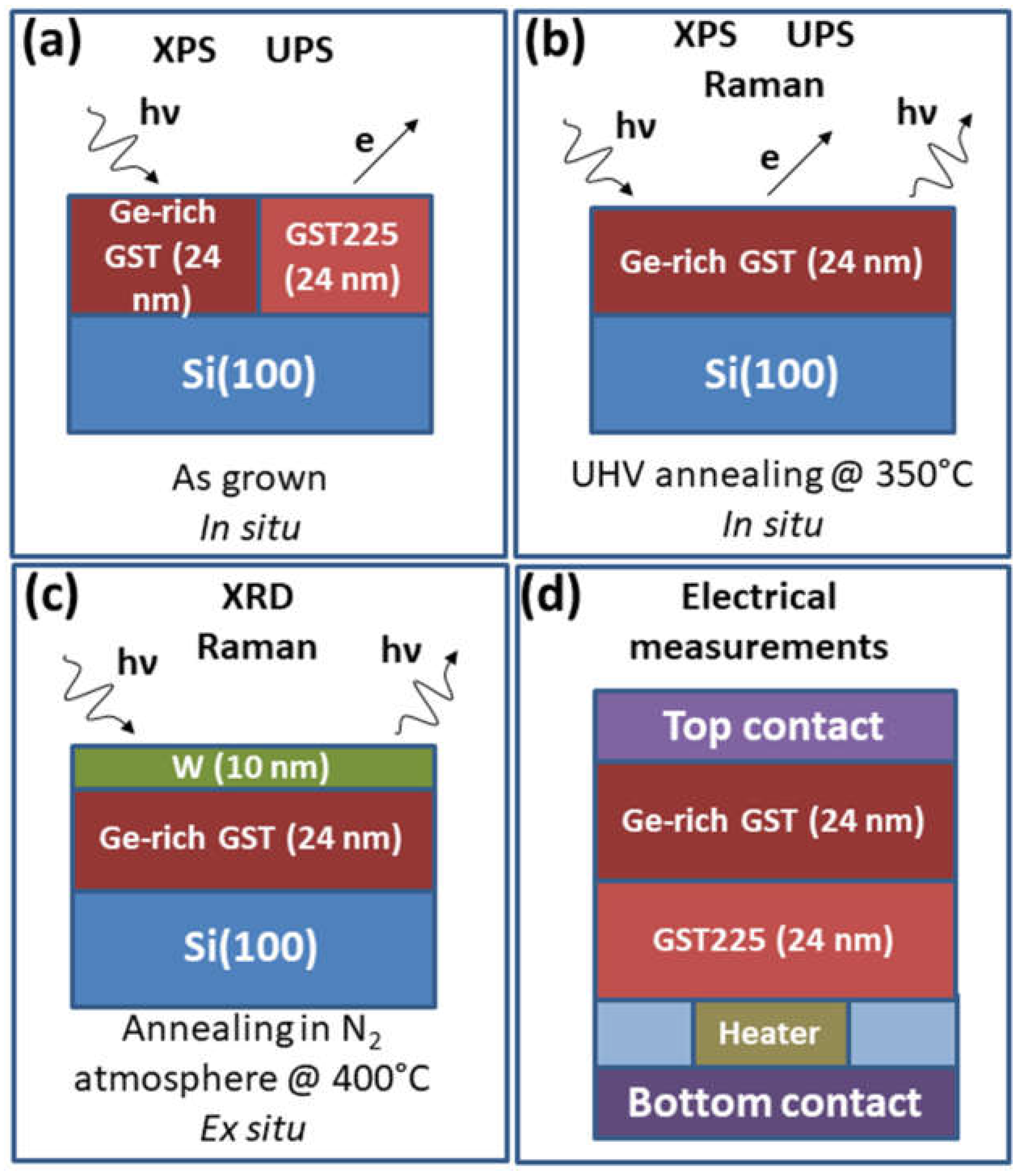
Abstract
:1. Introduction
2. Experimental
2.1. Sample Growth
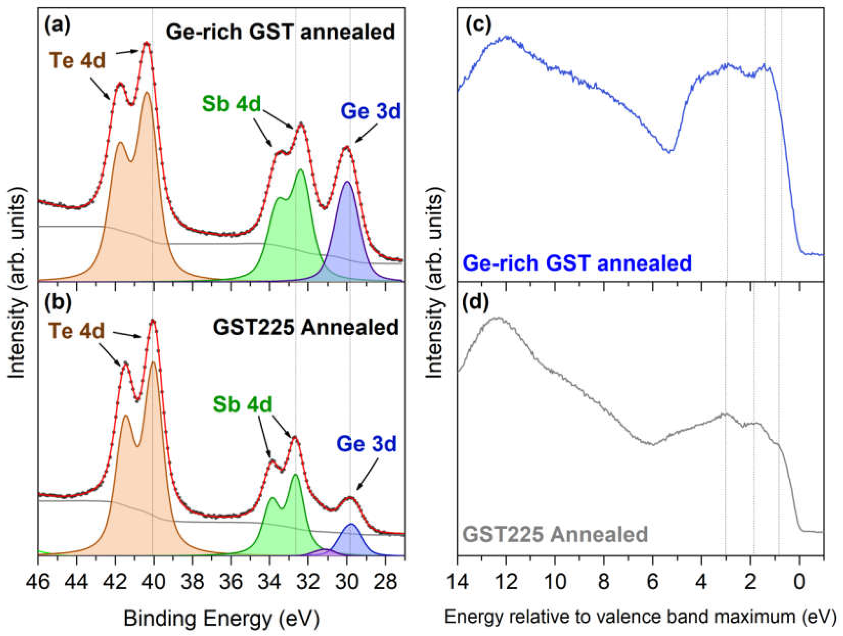
2.2. Photoemission Characterization
2.3. X-ray Diffraction
2.4. Raman
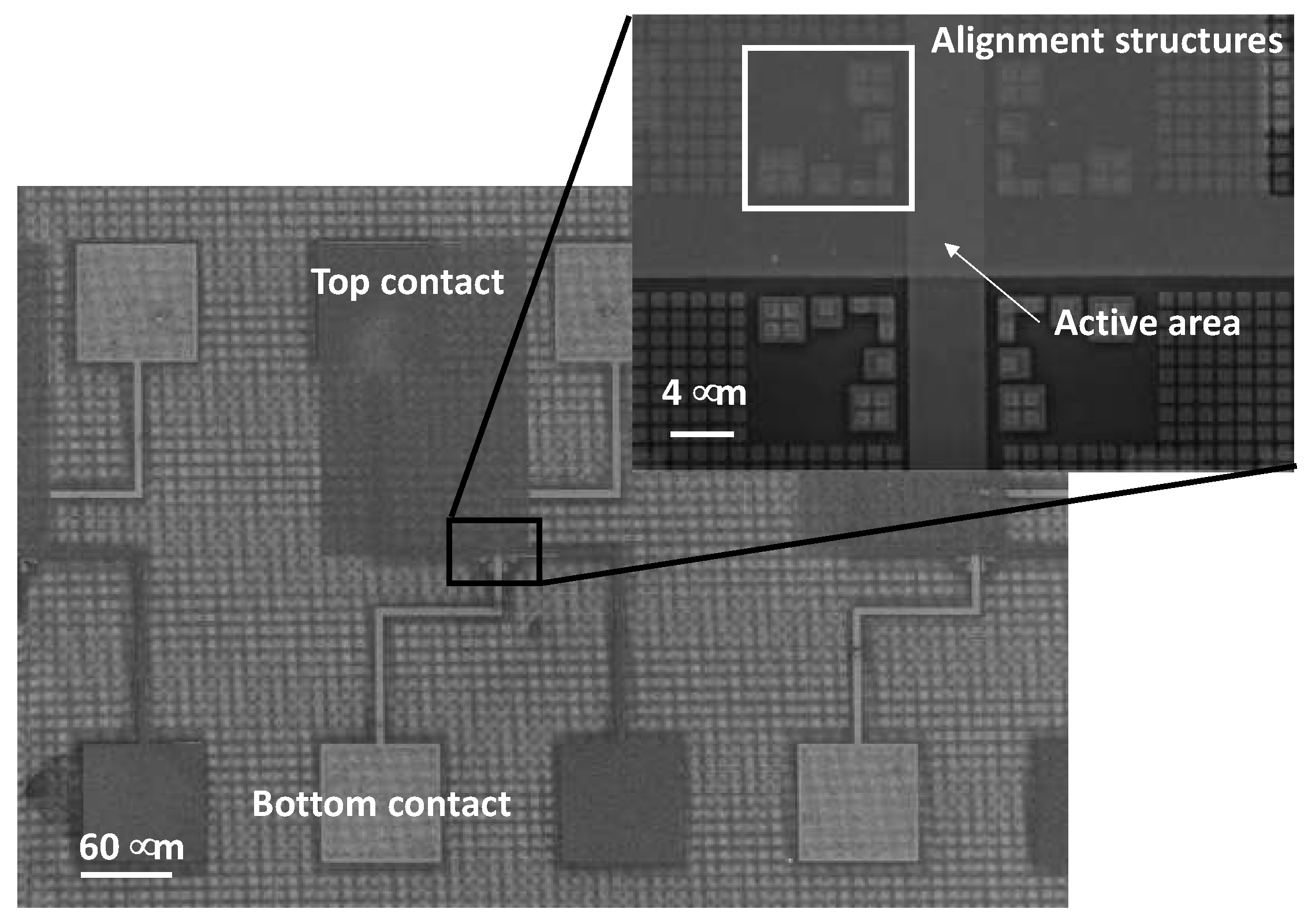
2.5. Memory Device Realization
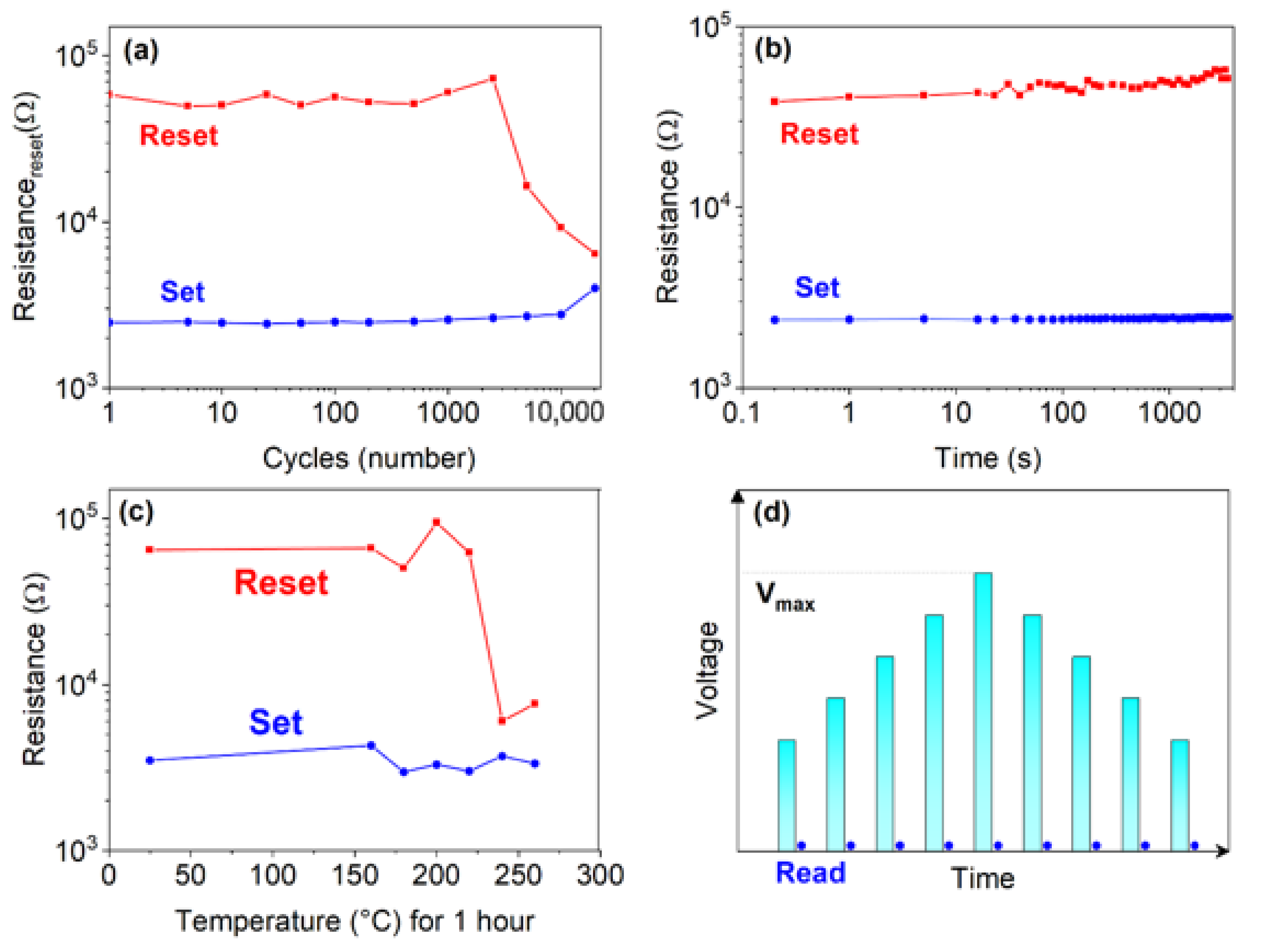
2.6. Electrical Measurements
3. Results and Discussion
4. Conclusions
Author Contributions
Funding
Conflicts of Interest
References
- Bandyopadhyay, D.; Sen, J. Internet of Things: Applications and Challenges in Technology and Standardization. Wirel. Pers Commun. 2011, 58, 49–69. [Google Scholar] [CrossRef]
- Cappelletti, P.; Annunziata, R.; Arnaud, F.; Disegni, F.; Maurelli, A.; Zuliani, P. Phase Change Memory for Automotive Grade Embedded NVM Applications. J. Phys. D Appl. Phys. 2020, 53, 193002. [Google Scholar] [CrossRef]
- Wuttig, M.; Yamada, N. Phase-Change Materials for Rewriteable Data Storage. Natur. Mater. 2007, 6, 824–832. [Google Scholar] [CrossRef] [PubMed]
- Fantini, A.; Perniola, L.; Armand, M.; Nodin, J.F.; Sousa, V.; Persico, A.; Cluzel, J.; Jahan, C.; Maitrejean, S.; Lhostis, S.; et al. Comparative Assessment of GST and GeTe Materials for Application to Embedded Phase-Change Memory Devices. In Proceedings of the 2009 IEEE International Memory Workshop, Monterey, CA, USA, 10–14 May 2009; pp. 1–2. [Google Scholar]
- Hubert, Q.; Jahan, C.; Toffoli, A.; Navarro, G.; Chandrashekar, S.; Noe, P.; Blachier, D.; Sousa, V.; Perniola, L.; Nodin, J.-F.; et al. Lowering the Reset Current and Power Consumption of Phase-Change Memories with Carbon-Doped Ge2Sb2Te5. In Proceedings of the 2012 4th IEEE International Memory Workshop, Milan, Italy, 20–23 May 2012; pp. 1–4. [Google Scholar]
- Li, T.; Shen, J.; Wu, L.; Song, Z.; Lv, S.; Cai, D.; Zhang, S.; Guo, T.; Song, S.; Zhu, M. Atomic-Scale Observation of Carbon Distribution in High-Performance Carbon-Doped Ge 2 Sb 2 Te 5 and Its Influence on Crystallization Behavior. J. Phys. Chem. C. 2019, 123, 13377–13384. [Google Scholar] [CrossRef]
- Kikuchi, S.; Oh, D.Y.; Kimura, I.; Nishioka, Y.; Ueda, M.; Endo, M.; Kokaze, Y.; Suu, K. Preparation of Oxygen-Doped and Nitrogen-Doped Ge-Sb-Te System Thin Film for Phase Change Random Access Memory by RF Magnetron Sputtering. In Proceedings of the 2006 7th Annual Non-Volatile Memory Technology Symposium, San Mateo, CA, USA, 5–8 November 2006; pp. 81–83. [Google Scholar]
- Privitera, S.; Rimini, E.; Zonca, R. Amorphous-to-Crystal Transition of Nitrogen- and Oxygen-Doped Ge2Sb2Te5 Films Studied by in Situ Resistance Measurements. Appl. Phys. Lett. 2004, 85, 3044–3046. [Google Scholar] [CrossRef]
- Lai, Y.; Qiao, B.; Feng, J.; Ling, Y.; Lai, L.; Lin, Y.; Tang, T.; Cai, B.; Chen, B. Nitrogen-Doped Ge2Sb2Te5 Films for Nonvolatile Memory. J. Elec. Mater. 2005, 34, 176–181. [Google Scholar] [CrossRef]
- Horii, H.; Yi, J.H.; Park, J.H.; Ha, Y.H.; Baek, I.G.; Park, S.O.; Hwang, Y.N.; Lee, S.H.; Kim, Y.T.; Lee, K.H.; et al. A Novel Cell Technology Using N-Doped GeSbTe Films for Phase Change RAM. In Proceedings of the 2003 Symposium on VLSI Technology. Digest of Technical Papers (IEEE Cat. No.03CH37407), Kyoto, Japan, 10–12 June 2003; pp. 177–178. [Google Scholar]
- Zuliani, P.; Varesi, E.; Palumbo, E.; Borghi, M.; Tortorelli, I.; Erbetta, D.; Libera, G.D.; Pessina, N.; Gandolfo, A.; Prelini, C.; et al. Overcoming Temperature Limitations in Phase Change Memories With Optimized GexSbyTez. IEEE Trans. Electron. Devices 2013, 60, 4020–4026. [Google Scholar] [CrossRef]
- Privitera, S.M.S.; López García, I.; Bongiorno, C.; Sousa, V.; Cyrille, M.C.; Navarro, G.; Sabbione, C.; Carria, E.; Rimini, E. Crystallization Properties of Melt-Quenched Ge-Rich GeSbTe Thin Films for Phase Change Memory Applications. J. Appl. Phys. 2020, 128, 155105. [Google Scholar] [CrossRef]
- Redaelli, A.; Petroni, E.; Annunziata, R. Material and Process Engineering Challenges in Ge-Rich GST for Embedded PCM. Mater. Sci. Semicond. Process. 2022, 137, 106184. [Google Scholar] [CrossRef]
- Tae Kim, Y.; Kim, S.-I. Comparison of Thermal Stabilities between Ge-Sb-Te and In-Sb-Te Phase Change Materials. Appl. Phys. Lett. 2013, 103, 121906. [Google Scholar] [CrossRef]
- Morikawa, T.; Kurotsuchi, K.; Kinoshita, M.; Matsuzaki, N.; Matsui, Y.; Fujisaki, Y.; Hanzawa, S.; Kotabe, M.; Moriya, H.; Iwasaki, T.; et al. Doped In-Ge-Te Phase Change Memory Featuring Stable Operation and Good Data Retention. In Proceedings of the 2007 IEEE International Electron Devices Meeting, Washington, DC, USA, 10 December 2007; pp. 307–310. [Google Scholar]
- Fallica, R.; Stoycheva, T.; Wiemer, C.; Longo, M. Structural and Electrical Analysis of In Sb Te-based PCM cells. Physica status solidi (RRL). Rapid Res. Lett. 2013, 7, 1009–1013. Available online: https://onlinelibrary.wiley.com/doi/abs/10.1002/pssr.201308074 (accessed on 20 March 2022).
- Selmo, S.; Cecchini, R.; Cecchi, S.; Wiemer, C.; Fanciulli, M.; Rotunno, E.; Lazzarini, L.; Rigato, M.; Pogany, D.; Lugstein, A.; et al. Low Power Phase Change Memory Switching of Ultra-Thin In3Sb1Te2 Nanowires. Appl. Phys. Lett. 2016, 109, 213103. [Google Scholar] [CrossRef]
- Cecchini, R.; Selmo, S.; Wiemer, C.; Rotunno, E.; Lazzarini, L.; De Luca, M.; Zardo, I.; Longo, M. Single-Step Au-Catalysed Synthesis and Microstructural Characterization of Core–Shell Ge/In–Te Nanowires by MOCVD. Mater. Res. Lett. 2018, 6, 29–35. [Google Scholar] [CrossRef] [Green Version]
- Chèze, C.; Righi Riva, F.; Di Bella, G.; Placidi, E.; Prili, S.; Bertelli, M.; Diaz Fattorini, A.; Longo, M.; Calarco, R.; Bernasconi, M.; et al. Interface Formation during the Growth of Phase Change Material Heterostructures Based on Ge-Rich Ge-Sb-Te Alloys. Nanomaterials 2022, 12, 1007. [Google Scholar] [CrossRef]
- Nolot, E.; Sabbione, C.; Pessoa, W.; Prazakova, L.; Navarro, G. Germanium, Antimony, Tellurium, Their Binary and Ternary Alloys and the Impact of Nitrogen: An X-Ray Photoelectron Study. Appl. Surf. Sci. 2021, 536, 147703. [Google Scholar] [CrossRef]
- Klein, A.; Dieker, H.; Späth, B.; Fons, P.; Kolobov, A.; Steimer, C.; Wuttig, M. Changes in Electronic Structure and Chemical Bonding upon Crystallization of the Phase Change Material GeSb2Te4. Phys. Rev. Lett. 2008, 100, 1–4. [Google Scholar] [CrossRef]
- Baeck, J.H.; Ann, Y.; Jeong, K.-H.; Cho, M.-H.; Ko, D.-H.; Oh, J.-H.; Jeong, H. Electronic Structure of Te/Sb/Ge and Sb/Te/Ge Multi Layer Films Using Photoelectron Spectroscopy. J. Am. Chem. Soc. 2009, 131, 13634–13638. [Google Scholar] [CrossRef]
- Kim, J.-J.; Kobayashi, K.; Ikenaga, E.; Kobata, M.; Ueda, S.; Matsunaga, T.; Kifune, K.; Kojima, R.; Yamada, N. Electronic Structure of Amorphous and Crystalline (GeTe)1−x(Sb2Te3)x Investigated Using Hard X-ray Photoemission Spectroscopy. Phys. Rev. B 2007, 76, 115124. [Google Scholar] [CrossRef]
- Lee, Y.M.; Jung, M.-C.; Shin, H.J.; Kim, K.; Song, S.A.; Jeong, H.S.; Ko, C.; Han, M. Temperature-Dependent High-Resolution X-Ray Photoelectron Spectroscopic Study on Ge1Sb2Te4. Thin Solid Films 2010, 518, 5670–5672. [Google Scholar] [CrossRef]
- Sosso, G.C.; Caravati, S.; Gatti, C.; Assoni, S.; Bernasconi, M. Vibrational Properties of Hexagonal Ge2Sb 2Te5 from First Principles. J. Phys. Condens. Matter 2009, 21, 245401. [Google Scholar] [CrossRef]
- Abou El Kheir, O.; Dragoni, D.; Bernasconi, M. Density Functional Simulations of Decomposition Pathways of Ge-Rich GeSbTe Alloys for Phase Change Memories. Phys. Rev. Mater. 2021, 5, 095004. [Google Scholar] [CrossRef]
- Abou El Kheir, O.; Bernasconi, M. High-Throughput Calculations on the Decomposition Reactions of Off-Stoichiometry GeSbTe Alloys for Embedded Memories. Nanomaterials 2021, 11, 2382. [Google Scholar] [CrossRef]
- Zuliani, P.; Palumbo, E.; Borghi, M.; Dalla Libera, G.; Annunziata, R. Engineering of Chalcogenide Materials for Embedded Applications of Phase Change Memory. Solid-State Electron. 2015, 111, 27–31. [Google Scholar] [CrossRef]
- Bragaglia, V.; Holldack, K.; Boschker, J.E.; Arciprete, F.; Zallo, E.; Flissikowski, T.; Calarco, R. Far-Infrared and Raman Spectroscopy Investigation of Phonon Modes in Amorphous and Crystalline Epitaxial GeTe-Sb2Te3 Alloys. Sci. Rep. 2016, 6, 28560. [Google Scholar] [CrossRef] [Green Version]
- Kumar, A.; Cecchini, R.; Wiemer, C.; Mussi, V.; De Simone, S.; Calarco, R.; Scuderi, M.; Nicotra, G.; Longo, M. Phase Change Ge-Rich Ge–Sb–Te/Sb2Te3 Core-Shell Nanowires by Metal Organic Chemical Vapor Deposition. Nanomaterials 2021, 11, 3358. [Google Scholar] [CrossRef]
- Di Biagio, F.; Cecchi, S.; Arciprete, F.; Calarco, R. Crystallization Study of Ge-Rich (GeTe)m(Sb2Te3) n Using Two-Step Annealing Process. Phys. Status Solidi RRL 2019, 13, 1800632. [Google Scholar] [CrossRef]
- Lannin, J.S.; Maley, N.; Kshirsagar, S.T. Raman scattering and short range order in amorphous germanium. Solid State Commun. 1985, 53, 939–942. [Google Scholar] [CrossRef]
- Kazimierski, P.; Tyczkowski, J.; Kozanecki, M.; Hatanaka, Y.; Aoki, T. Transition from Amorphous Semiconductor to Amorphous Insulator in Hydrogenated Carbon−Germanium Films Investigated by Raman Spectroscopy. Chem. Mater. 2002, 14, 4694–4701. [Google Scholar] [CrossRef]
- Jamali, H.; Mozafarinia, R.; Eshaghi, A. The Effect of Carbon Content on the Phase Structure of Amorphous/Nanocrystalline Ge1−xCx Films Prepared by PECVD. Surf. Coat. Technol. 2017, 310, 1–7. [Google Scholar] [CrossRef]
- Prazakova, L.; Nolot, E.; Martinez, E.; Rouchon, D.; Fillot, F.; Bernier, N.; Elizalde, R.; Bernard, M.; Navarro, G. The Effect of Ge Content on Structural Evolution of Ge-Rich GeSbTe Alloys at Increasing Temperature. Materialia 2022, 21, 101345. [Google Scholar] [CrossRef]
- Cecchi, S.; Lopez Garcia, I.; Mio, A.M.; Zallo, E.; Abou El Kheir, O.; Calarco, R.; Bernasconi, M.; Nicotra, G.; Privitera, S.M.S. Crystallization and Electrical Properties of Ge-Rich GeSbTe Alloys. Nanomaterials 2022, 12, 631. [Google Scholar] [CrossRef] [PubMed]
- Goriparti, S.; Miele, E.; Scarpellini, A.; Marras, S.; Prato, M.; Ansaldo, A.; DeAngelis, F.; Manna, L.; Zaccaria, R.P.; Capiglia, C. Germanium Nanocrystals-MWCNTs Composites as Anode Materials for Lithium Ion Batteries. ECS Trans. 2014, 62, 19–24. [Google Scholar] [CrossRef]
- Sousa, V.; Navarro, G.; Castellani, N.; Coue, M.; Cueto, O.; Sabbione, C.; Noe, P.; Perniola, L.; Blonkowski, S.; Zuliani, P.; et al. Operation Fundamentals in 12Mb Phase Change Memory Based on Innovative Ge-Rich GST Materials Featuring High Reliability Performance. In Proceedings of the 2015 Symposium on VLSI Technology (VLSI Technology), Kyoto, Japan, 16–18 June 2015; pp. T98–T99. [Google Scholar]
- Kiouseloglou, A.; Navarro, G.; Sousa, V.; Persico, A.; Roule, A.; Cabrini, A.; Torelli, G.; Maitrejean, S.; Reimbold, G.; De Salvo, B.; et al. A Novel Programming Technique to Boost Low-Resistance State Performance in Ge-Rich GST Phase Change Memory. IEEE Trans. Electron. Devices 2014, 61, 1246–1254. [Google Scholar] [CrossRef]


Publisher’s Note: MDPI stays neutral with regard to jurisdictional claims in published maps and institutional affiliations. |
© 2022 by the authors. Licensee MDPI, Basel, Switzerland. This article is an open access article distributed under the terms and conditions of the Creative Commons Attribution (CC BY) license (https://creativecommons.org/licenses/by/4.0/).
Share and Cite
Díaz Fattorini, A.; Chèze, C.; López García, I.; Petrucci, C.; Bertelli, M.; Righi Riva, F.; Prili, S.; Privitera, S.M.S.; Buscema, M.; Sciuto, A.; et al. Growth, Electronic and Electrical Characterization of Ge-Rich Ge–Sb–Te Alloy. Nanomaterials 2022, 12, 1340. https://doi.org/10.3390/nano12081340
Díaz Fattorini A, Chèze C, López García I, Petrucci C, Bertelli M, Righi Riva F, Prili S, Privitera SMS, Buscema M, Sciuto A, et al. Growth, Electronic and Electrical Characterization of Ge-Rich Ge–Sb–Te Alloy. Nanomaterials. 2022; 12(8):1340. https://doi.org/10.3390/nano12081340
Chicago/Turabian StyleDíaz Fattorini, Adriano, Caroline Chèze, Iñaki López García, Christian Petrucci, Marco Bertelli, Flavia Righi Riva, Simone Prili, Stefania M. S. Privitera, Marzia Buscema, Antonella Sciuto, and et al. 2022. "Growth, Electronic and Electrical Characterization of Ge-Rich Ge–Sb–Te Alloy" Nanomaterials 12, no. 8: 1340. https://doi.org/10.3390/nano12081340