
Physical Operations of a Self-Powered IZTO/β-Ga2O3 Schottky Barrier Diode Photodetector

 , and
, and
Abstract
:1. Introduction
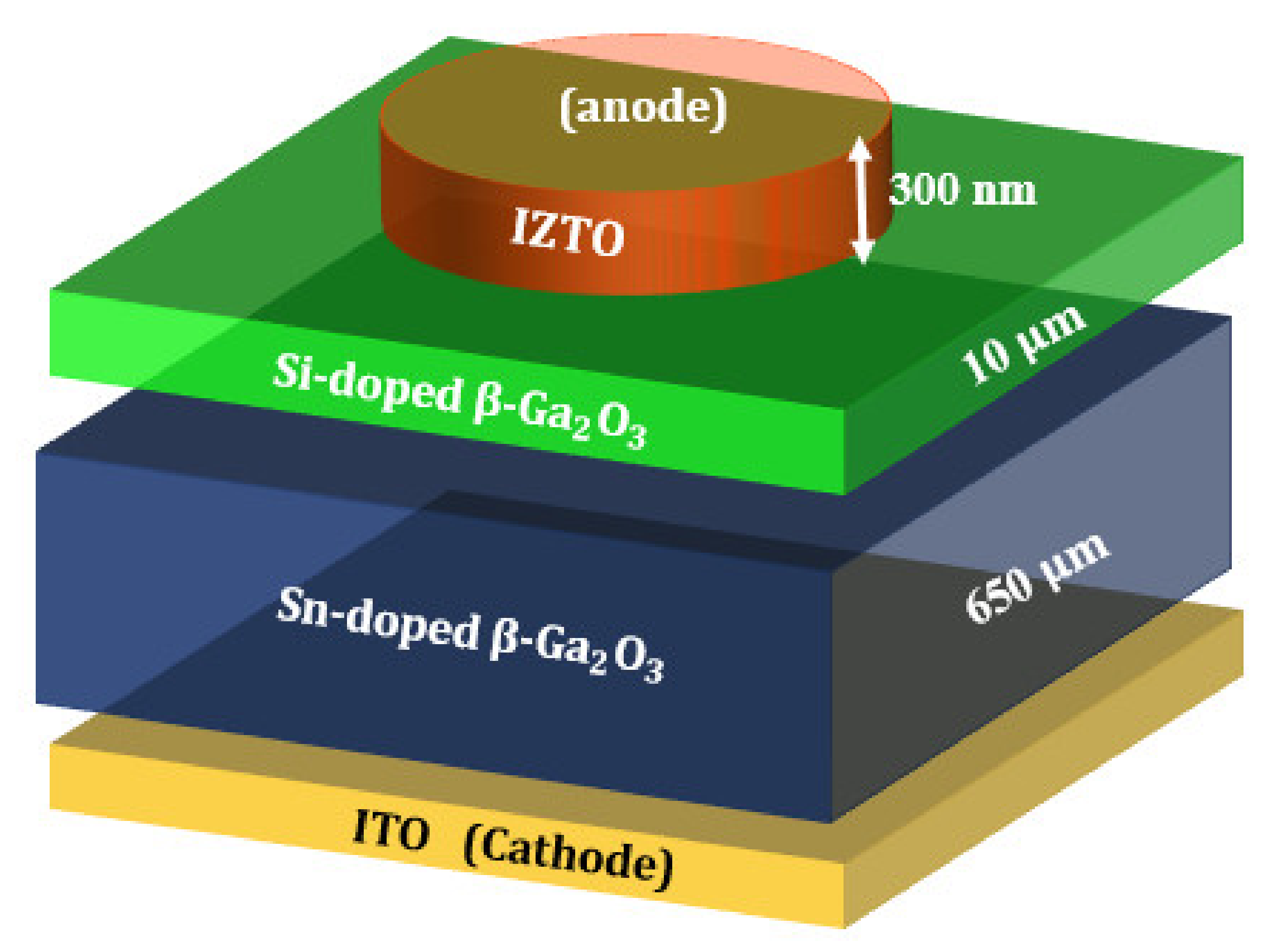
2. Experiment
3. Simulation Methodology
4. Results and Discussion
4.1. Optical and Electrical Properties of IZTO Thin Film
4.2. Modeling the Dark Current of IZTO/β-Ga2O3 SBD
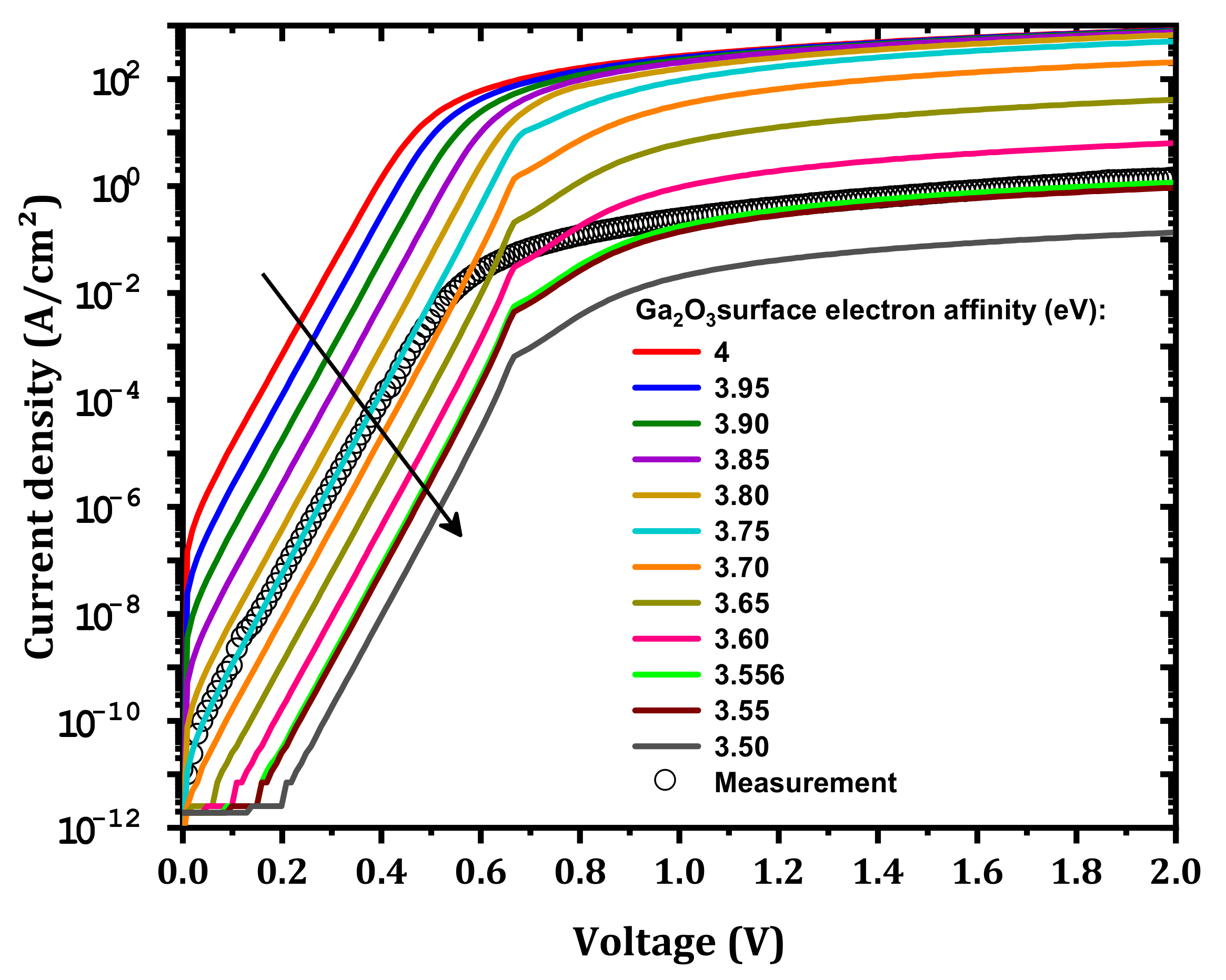
4.3. Effect of IL Electron Affinity
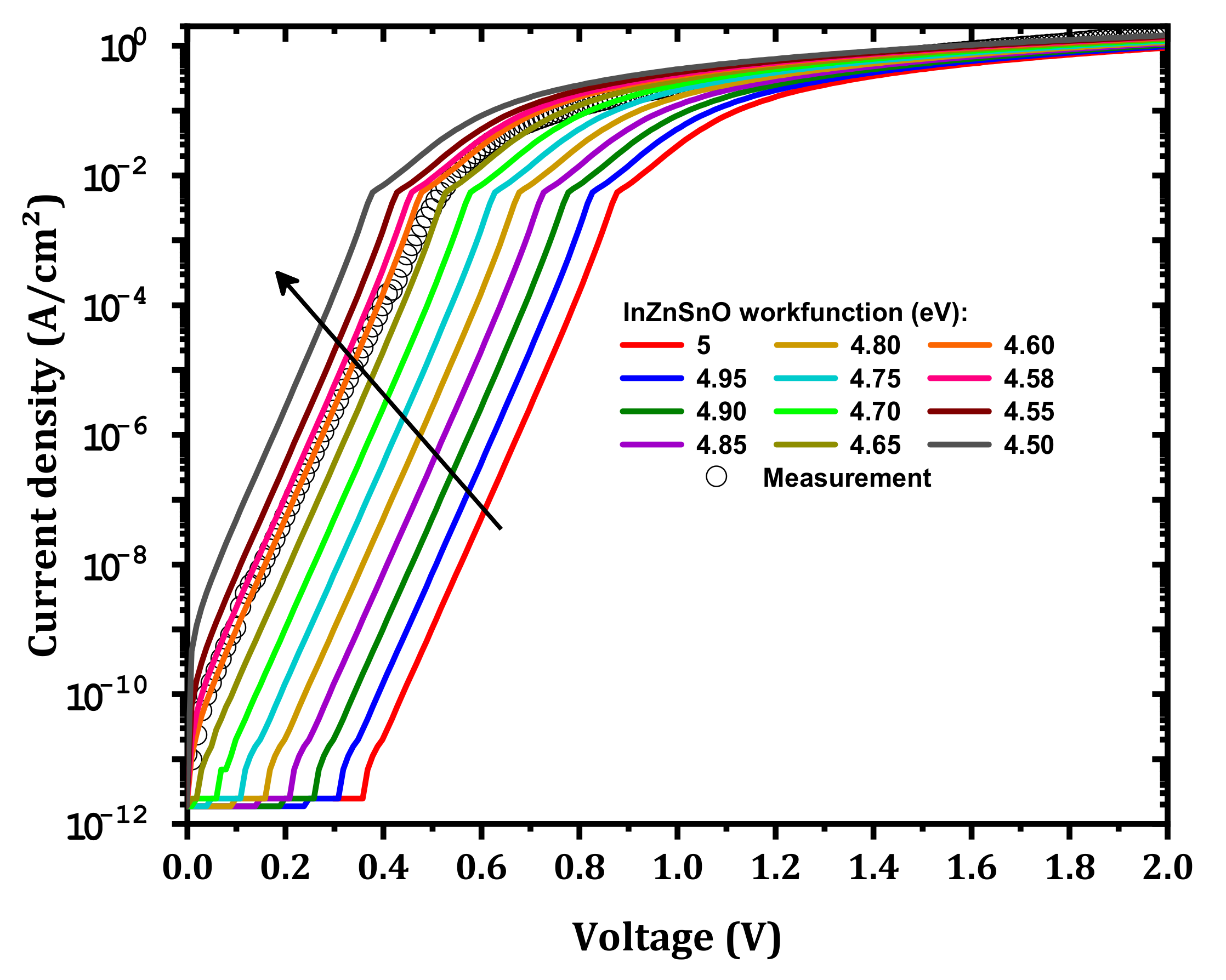
4.4. Effect of the IZTO Workfunction
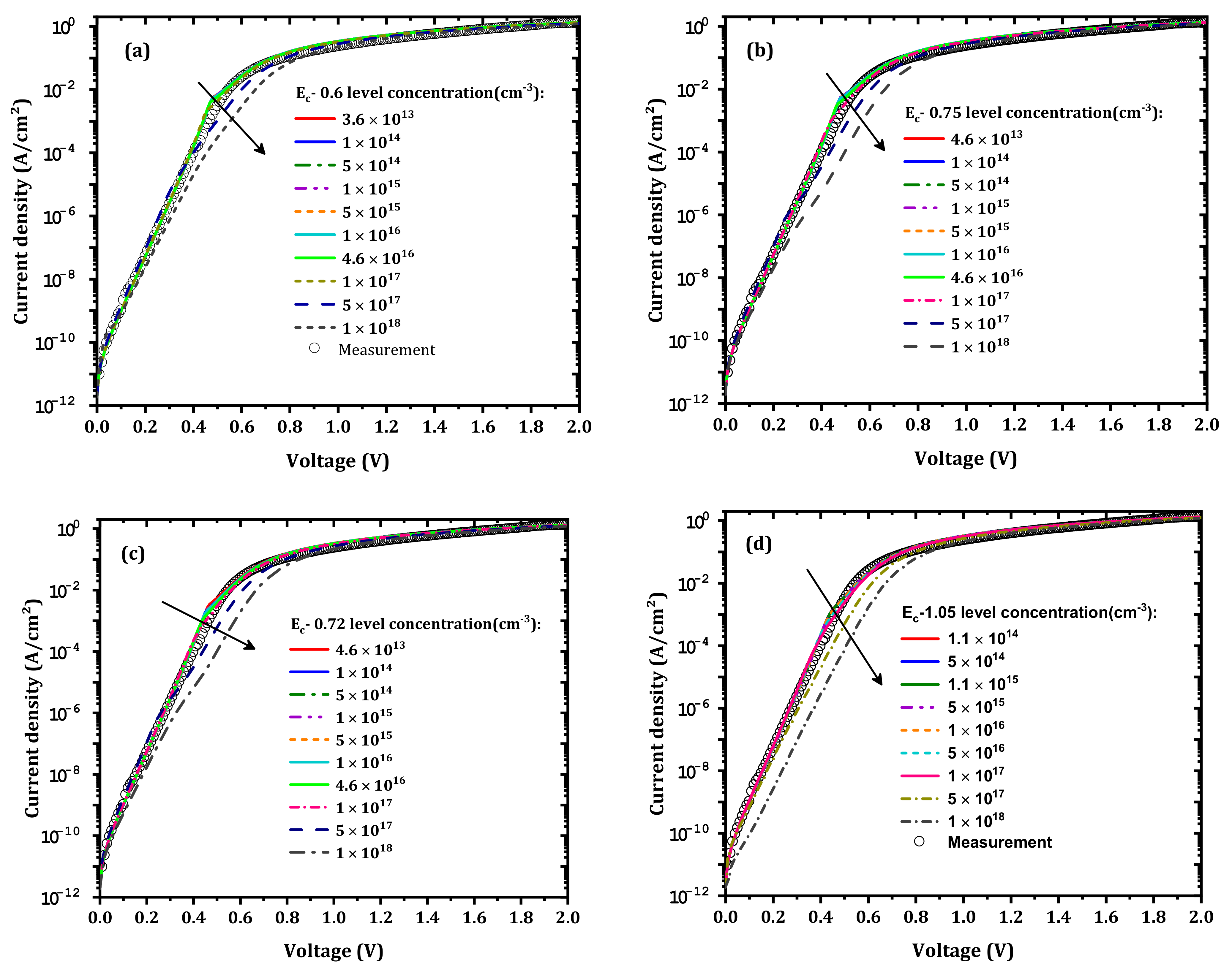
4.5. Effect of the Concentration of Traps at the IL
4.6. The Effect of 255 nm Wavelength Illumination on Forward Current
5. Conclusions
Author Contributions
Funding
Institutional Review Board Statement
Informed Consent Statement
Data Availability Statement
Acknowledgments
Conflicts of Interest
References
- Galazka, Z. β-Ga2O3 for wide-bandgap electronics and optoelectronics. Semicond. Sci. Technol. 2018, 33, 113001. [Google Scholar] [CrossRef]
- Labed, M.; Sengouga, N.; Labed, M.; Meftah, A.; Kyoung, S.; Kim, H.; Rim, Y.S. Modeling a Ni/β-Ga2O3 Schottky barrier diode deposited by confined magnetic-field-based sputtering. J. Phys. D Appl. Phys. 2021, 54, 115102. [Google Scholar] [CrossRef]
- Labed, M.; Sengouga, N.; Labed, M.; Meftah, A.; Kyoung, S.; Kim, H.; Rim, Y.S. Modeling and analyzing temperature-dependent parameters of Ni/β-Ga2O3 Schottky barrier diode deposited by confined magnetic field-based sputtering. Semicond. Sci. Technol. 2021, 36, 35020. [Google Scholar] [CrossRef]
- Labed, M.; Sengouga, N.; Meftah, A.; Labed, M.; Kyoung, S.; Kim, H.; Rim, Y.S. Leakage Current Modelling and Optimization of β-Ga2O3 Schottky Barrier Diode with Ni Contact under High Reverse Voltage. ECS J. Solid State Sci. Technol. 2020, 9, 125001. [Google Scholar] [CrossRef]
- Pearton, S.J.; Ren, F.; Tadjer, M.; Kim, J. Perspective: Ga2O3 for ultra-high power rectifiers and MOSFETS. J. Appl. Phys. 2018, 124, 220901. [Google Scholar] [CrossRef] [Green Version]
- Thomas, S.R.; Adamopoulos, G.; Lin, Y.-H.; Faber, H.; Sygellou, L.; Stratakis, E.; Pliatsikas, N.; Patsalas, P.A.; Anthopoulos, T.D. High electron mobility thin-film transistors based on Ga2O3 grown by atmospheric ultrasonic spray pyrolysis at low temperatures. Appl. Phys. Lett. 2014, 105, 092105. [Google Scholar] [CrossRef]
- Grillo, A.; Barrat, J.; Galazka, Z.; Passacantando, M.; Giubileo, F.; Iemmo, L.; Luongo, G.; Urban, F.; Dubourdieu, C.; Di Bartolomeo, A. High field-emission current density from β-Ga2O3 nanopillars. Appl. Phys. Lett. 2019, 114, 193101. [Google Scholar] [CrossRef]
- Jian, G.; He, Q.; Mu, W.; Fu, B.; Dong, H.; Qin, Y.; Zhang, Y.; Xue, H.; Long, S.; Jia, Z.; et al. Characterization of the inhomogeneous barrier distribution in a Pt/(100)β-Ga2O3 Schottky diode via its temperature-dependent electrical properties. AIP Adv. 2018, 8, 015316. [Google Scholar] [CrossRef] [Green Version]
- Labed, M.; Park, J.H.; Meftah, A.; Sengouga, N.; Hong, J.Y.; Jung, Y.-K.; Rim, Y.S. Low Temperature Modeling of Ni/β-Ga2O3 Schottky Barrier Diode Interface. ACS Appl. Electron. Mater. 2021, 3, 3667–3673. [Google Scholar] [CrossRef]
- Peng, B.; Yuan, L.; Zhang, H.; Cheng, H.; Zhang, S.; Zhang, Y.; Zhang, Y.; Jia, R. Fast-response self-powered solar-blind photodetector based on Pt/β-Ga2O3 Schottky barrier diodes. Optik 2021, 245, 167715. [Google Scholar] [CrossRef]
- Kim, H.; Seok, H.-J.; Park, J.H.; Chung, K.-B.; Kyoung, S.; Kim, H.-K.; Rim, Y.S. Fully Transparent InZnSnO/β-Ga2O3/InSnO Solar-Blind Photodetectors with High Schottky Barrier Height and Low-Defect Interfaces. J. Alloys Compd. 2021, 890, 161931. [Google Scholar] [CrossRef]
- Guo, D.; Liu, H.; Li, P.; Wu, Z.; Wang, S.; Cui, C.; Li, C.; Tang, W. Zero-Power-Consumption Solar-Blind Photodetector Based on β-Ga2O3/NSTO Heterojunction. ACS Appl. Mater. Interfaces 2017, 9, 1619–1628. [Google Scholar] [CrossRef] [PubMed]
- Qin, Y.; Li, L.; Zhao, X.; Tompa, G.S.; Dong, H.; Jian, G.; He, Q.; Tan, P.; Hou, X.; Zhang, Z.; et al. Metal–Semiconductor–Metal ε-Ga2O3 Solar-Blind Photodetectors with a Record-High Responsivity Rejection Ratio and Their Gain Mechanism. ACS Photonics 2020, 7, 812–820. [Google Scholar] [CrossRef]
- Zhuo, R.; Wu, D.; Wang, Y.; Wu, E.; Jia, C.; Shi, Z.; Xu, T.; Tian, Y.; Li, X. A self-powered solar-blind photodetector based on a MoS2/β-Ga2O3 heterojunction. J. Mater. Chem. C 2018, 6, 10982–10986. [Google Scholar] [CrossRef]
- Liu, Z.; Wang, X.; Liu, Y.; Guo, D.; Li, S.; Yan, Z.; Tan, C.-K.; Li, W.; Li, P.; Tang, W. A high-performance ultraviolet solar-blind photodetector based on a β-Ga2O3 Schottky photodiode. J. Mater. Chem. C 2019, 7, 13920–13929. [Google Scholar] [CrossRef]
- Zou, Y.; Zhang, Y.; Hu, Y.; Gu, H. Ultraviolet Detectors Based on Wide Bandgap Semiconductor Nanowire: A Review. Sensors 2018, 18, 2072. [Google Scholar] [CrossRef] [Green Version]
- Chen, Y.; Zhang, K.; Yang, X.; Chen, X.; Sun, J.; Zhao, Q.; Li, K.; Shan, C. Solar-blind photodetectors based on MXenes–β-Ga2O3 Schottky junctions. J. Phys. D Appl. Phys. 2020, 53, 484001. [Google Scholar] [CrossRef]
- Chen, X.; Liu, K.; Zhang, Z.; Wang, C.; Li, B.; Zhao, H.; Zhao, D.; Shen, D. Self-Powered Solar-Blind Photodetector with Fast Response Based on Au/β-Ga2O3 Nanowires Array Film Schottky Junction. ACS Appl. Mater. Interfaces 2016, 8, 4185–4191. [Google Scholar] [CrossRef]
- Zhi, Y.; Liu, Z.; Chu, X.; Li, S.; Yan, Z.; Wang, X.; Huang, Y.; Wang, J.; Wu, Z.; Guo, D.; et al. Self-Powered β-Ga2O3 Solar-Blind Photodetector Based on the Planar Au/Ga2O3 Schottky Junction. ECS J. Solid State Sci. Technol. 2020, 9, 65011. [Google Scholar] [CrossRef]
- Liu, Z.; Zhi, Y.; Zhang, S.; Li, S.; Yan, Z.; Gao, A.; Zhang, S.; Guo, D.; Wang, J.; Wu, Z.; et al. Ultrahigh-performance planar β-Ga2O3 solar-blind Schottky photodiode detectors. Sci. China Technol. Sci. 2021, 64, 59–64. [Google Scholar] [CrossRef]
- Cui, S.; Mei, Z.; Zhang, Y.; Liang, H.; Du, X. Room-Temperature Fabricated Amorphous Ga2O3 High-Response-Speed Solar-Blind Photodetector on Rigid and Flexible Substrates. Adv. Opt. Mater. 2017, 5, 1700454. [Google Scholar] [CrossRef]
- Labed, M.; Sengouga, N.; Meftah, A.; Meftah, A.; Rim, Y.S. Study on the improvement of the open-circuit voltage of NiOx/Si heterojunction solar cell. Opt. Mater. 2021, 120, 111453. [Google Scholar] [CrossRef]
- Polyakov, A.Y.; Lee, I.-H.; Smirnov, N.B.; Yakimov, E.B.; Shchemerov, I.V.; Chernykh, A.V.; Kochkova, A.I.; Vasilev, A.A.; Carey, P.H.; Ren, F.; et al. Defects at the surface of β-Ga2O3 produced by Ar plasma exposure. APL Mater. 2019, 7, 061102. [Google Scholar] [CrossRef] [Green Version]
- Labed, M.; Sengouga, N.; Rim, Y.S. Control of Ni/β-Ga2O3 Vertical Schottky Diode Output Parameters at Forward Bias by Insertion of a Graphene Layer. Nanomaterials 2022, 12, 827. [Google Scholar] [CrossRef]
- Sze, S.M.; Ng, K.K. Physics and Properties of Semiconductors—A Review. Phys. Semicond. Devices 2006, 3, 5–75. [Google Scholar]
- Carey, P.H.; Yang, J.; Ren, F.; Hays, D.C.; Pearton, S.J.; Kuramata, A.; Kravchenko, I.I. Improvement of Ohmic contacts on Ga2O3 through use of ITO-interlayers. J. Vac. Sci. Technol. B 2017, 35, 61201. [Google Scholar] [CrossRef]
- Oshima, T.; Wakabayashi, R.; Hattori, M.; Hashiguchi, A.; Kawano, N.; Sasaki, K.; Masui, T.; Kuramata, A.; Yamakoshi, S.; Yoshimatsu, K.; et al. Formation of indium–tin oxide ohmic contacts for β-Ga2O3. Jpn. J. Appl. Phys. 2016, 55, 1202B7. [Google Scholar] [CrossRef]
- Li, K.-D.; Chen, P.-W.; Chang, K.-S.; Hsu, S.-C.; Jan, D.-J. Indium-Zinc-Tin-Oxide Film Prepared by Reactive Magnetron Sputtering for Electrochromic Applications. Materials 2018, 11, 2221. [Google Scholar] [CrossRef] [Green Version]
- Hakkoum, H.; Tibermacine, T.; Sengouga, N.; Belahssen, O.; Ghougali, M.; Benhaya, A.; Moumen, A.; Comini, E. Effect of the source solution quantity on optical characteristics of ZnO and NiO thin films grown by spray pyrolysis for the design NiO/ZnO photodetectors. Opt. Mater. 2020, 108, 110434. [Google Scholar] [CrossRef]
- Hassanien, A.S.; Akl, A.A. Influence of composition on optical and dispersion parameters of thermally evaporated non-crystalline Cd50S50−xSex thin films. J. Alloys Compd. 2015, 648, 280–290. [Google Scholar] [CrossRef]
- Yang, W.-C.; Rodriguez, B.J.; Gruverman, A.; Nemanich, R.J. Polarization-dependent electron affinity of LiNbO3 surfaces. Appl. Phys. Lett. 2004, 85, 2316–2318. [Google Scholar] [CrossRef] [Green Version]
- Mohamed, M.; Irmscher, K.; Janowitz, C.; Galazka, Z.; Manzke, R.; Fornari, R. Schottky barrier height of Au on the transparent semiconducting oxide β-Ga2O3. Appl. Phys. Lett. 2012, 101, 132106. [Google Scholar] [CrossRef]
- Lee, H.Y.; Lichtenwalner, D.J.; Jur, J.S.; Kingon, A.I. Investigation of Conducting Oxide and Metal Electrode Work Functions on Lanthanum Silicate High-k Dielectric. ECS Trans. 2019, 11, 607–612. [Google Scholar] [CrossRef]
- Choi, K.-H.; Nam, H.-J.; Jeong, J.-A.; Cho, S.-W.; Kim, H.-K.; Kang, J.-W.; Kim, D.-G.; Cho, W.-J. Highly flexible and transparent InZnSnOx∕Ag∕InZnSnOx multilayer electrode for flexible organic light emitting diodes. Appl. Phys. Lett. 2008, 92, 223302. [Google Scholar] [CrossRef]
- Buchholz, D.B.; Proffit, D.E.; Wisser, M.D.; Mason, T.O.; Chang, R.P.H. Electrical and band-gap properties of amorphous zinc–indium–tin oxide thin films. Prog. Nat. Sci. Mater. Int. 2012, 22, 1–6. [Google Scholar] [CrossRef] [Green Version]
- Sato, K.; Yasumura, Y. Study of forward I-V plot for Schottky diodes with high series resistance. J. Appl. Phys. 1985, 58, 3655–3657. [Google Scholar] [CrossRef]
- Hu, Q.; Wang, P.; Yin, J.; Liu, Y.; Lv, B.; Zhu, J.-L.; Dong, Z.; Zhang, W.; Ma, W.; Sun, J. High-Responsivity Photodetector Based on a Suspended Monolayer Graphene/RbAg4I5 Composite Nanostructure. ACS Appl. Mater. Interfaces 2020, 12, 50763–50771. [Google Scholar] [CrossRef]
- Periyanagounder, D.; Gnanasekar, P.; Varadhan, P.; He, J.-H.; Kulandaivel, J. High performance, self-powered photodetectors based on a graphene/silicon Schottky junction diode. J. Mater. Chem. C 2018, 6, 9545–9551. [Google Scholar] [CrossRef]
- Wu, D.; Zhao, Z.; Lu, W.; Rogée, L.; Zeng, L.; Lin, P.; Shi, Z.; Tian, Y.; Li, X.; Tsang, Y.H. Highly sensitive solar-blind deep ultraviolet photodetector based on graphene/PtSe2/β-Ga2O3 2D/3D Schottky junction with ultrafast speed. Nano Res. 2021, 14, 1973–1979. [Google Scholar] [CrossRef]


| Parameters | Sn: β-Ga2O3 | Si: β-Ga2O3 |
|---|---|---|
| Bandgap (eV) | 4.8 | 4.8 |
| Affinity (eV) | 4 | 4 |
| 10 | 10 | |
| 172 | 300 | |
| 0.28 | 0.28 | |
| 0.35 | 0.35 | |
| Relative permittivity | 12.6 | 11 |
| Minority carrier diffusion length (nm) | ||
| Saturation velocity (cm s⁻1) |
| Traps | Trap Level | Concentration | ||
|---|---|---|---|---|
| Sn-doped β-Ga2O3 Bulk layer | 0.55 | 100 | ||
| 0.74 | 100 | |||
| 1.04 | 10 | |||
| Si-doped β-Ga2O3 thin layer | 0.60 | 100 | ||
| 0.75 | 100 | |||
| 0.72 | 100 | |||
| 1.05 | 10 |
| Parameter | (Ω cm2) | ||||
|---|---|---|---|---|---|
| Simulation | 1.02 | 1.25 | 1.78 | 1.01 | |
| Measurement | 1.03 | 1.29 | 1.91 | 1.04 |
Publisher’s Note: MDPI stays neutral with regard to jurisdictional claims in published maps and institutional affiliations. |
© 2022 by the authors. Licensee MDPI, Basel, Switzerland. This article is an open access article distributed under the terms and conditions of the Creative Commons Attribution (CC BY) license (https://creativecommons.org/licenses/by/4.0/).
Share and Cite
Labed, M.; Kim, H.; Park, J.H.; Labed, M.; Meftah, A.; Sengouga, N.; Rim, Y.S. Physical Operations of a Self-Powered IZTO/β-Ga2O3 Schottky Barrier Diode Photodetector. Nanomaterials 2022, 12, 1061. https://doi.org/10.3390/nano12071061
Labed M, Kim H, Park JH, Labed M, Meftah A, Sengouga N, Rim YS. Physical Operations of a Self-Powered IZTO/β-Ga2O3 Schottky Barrier Diode Photodetector. Nanomaterials. 2022; 12(7):1061. https://doi.org/10.3390/nano12071061
Chicago/Turabian StyleLabed, Madani, Hojoong Kim, Joon Hui Park, Mohamed Labed, Afak Meftah, Nouredine Sengouga, and You Seung Rim. 2022. "Physical Operations of a Self-Powered IZTO/β-Ga2O3 Schottky Barrier Diode Photodetector" Nanomaterials 12, no. 7: 1061. https://doi.org/10.3390/nano12071061