
Application of Mini-LEDs with Microlens Arrays and Quantum Dot Film as Extra-Thin, Large-Area, and High-Luminance Backlight


Abstract
:1. Introduction
2. Methods
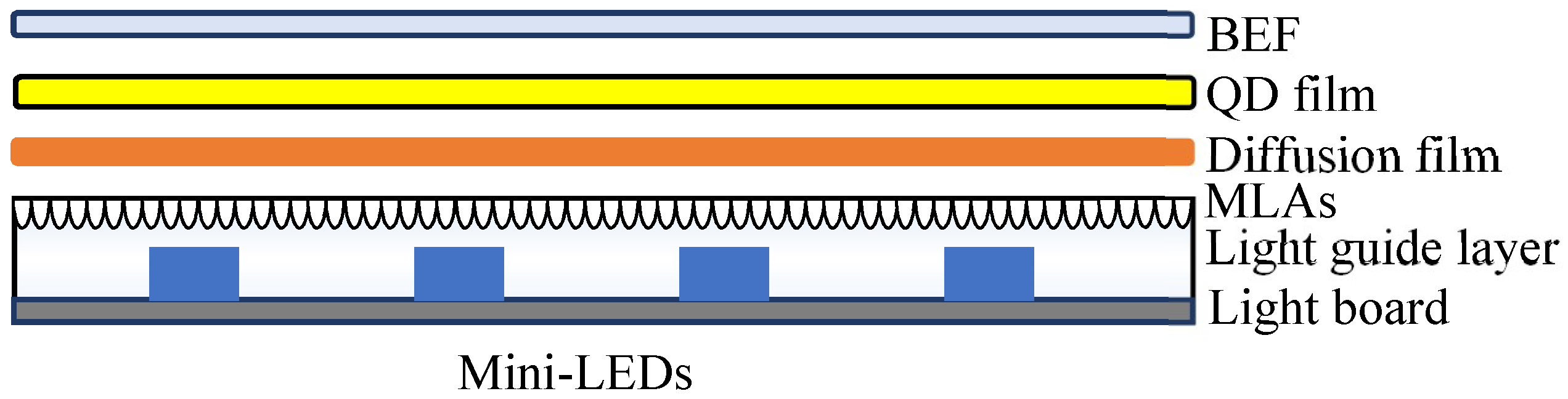
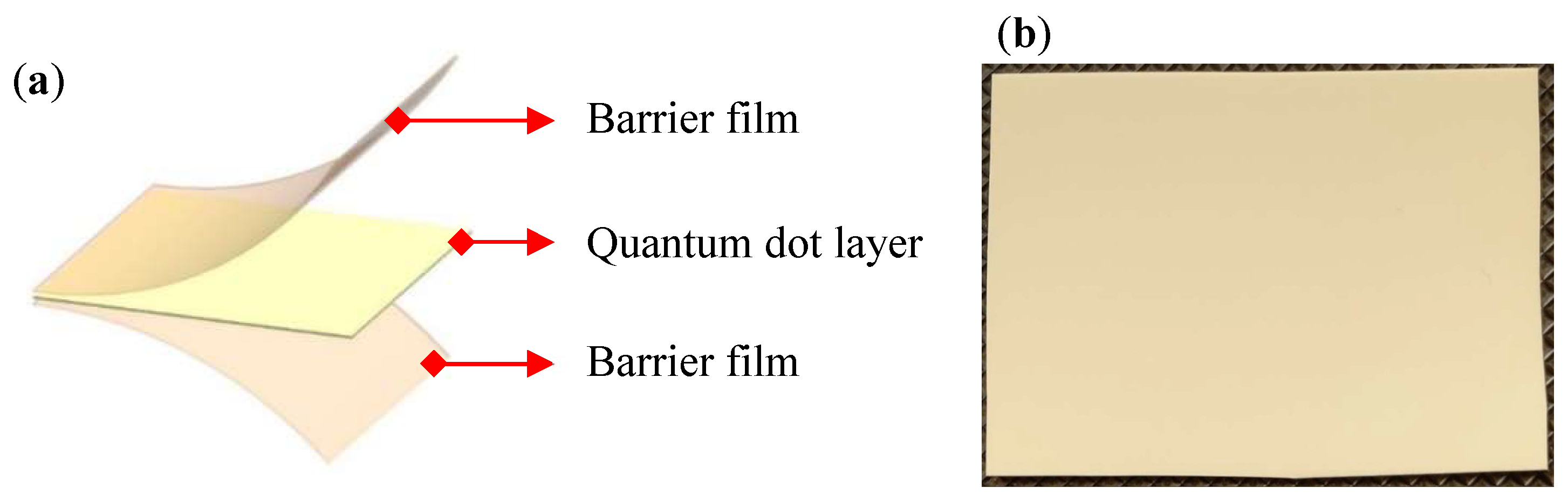
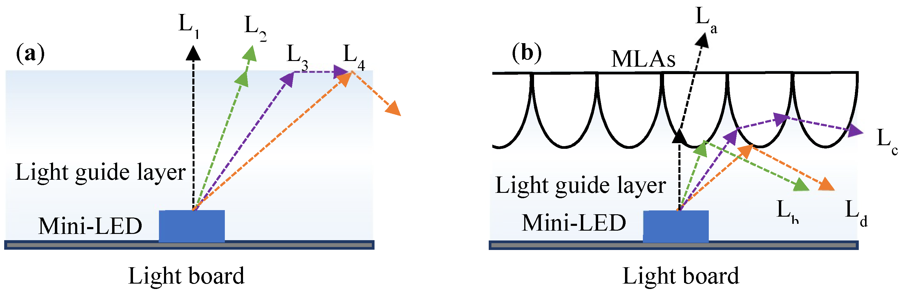
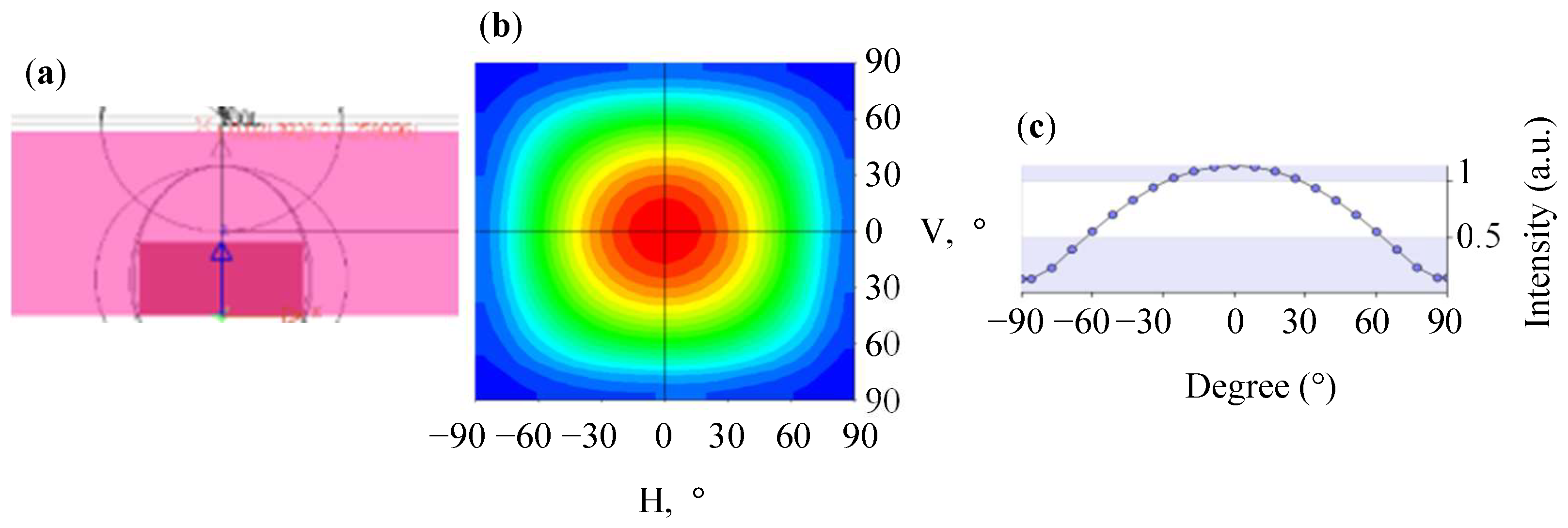
2.1. Simulation of Mini-LEDs with an MLA Unit Module and a Light Film Material Selection
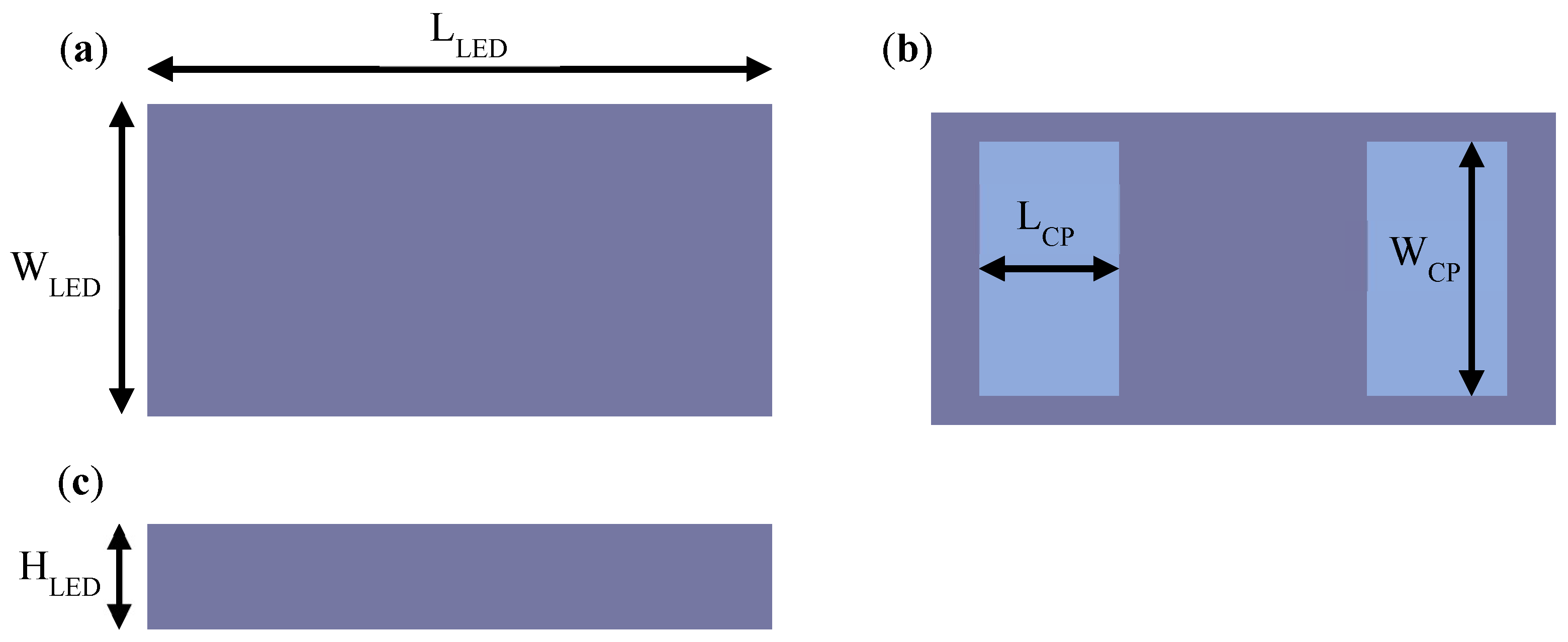
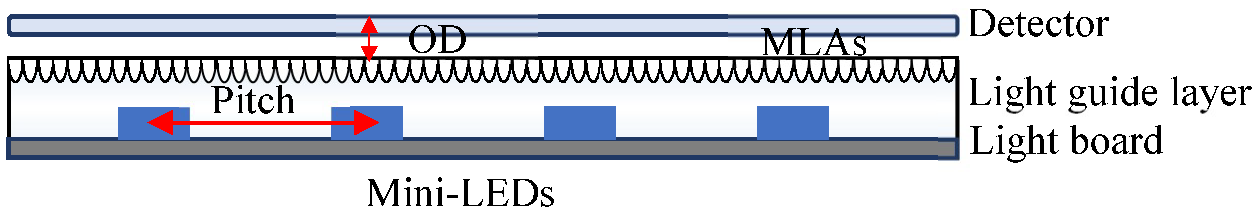
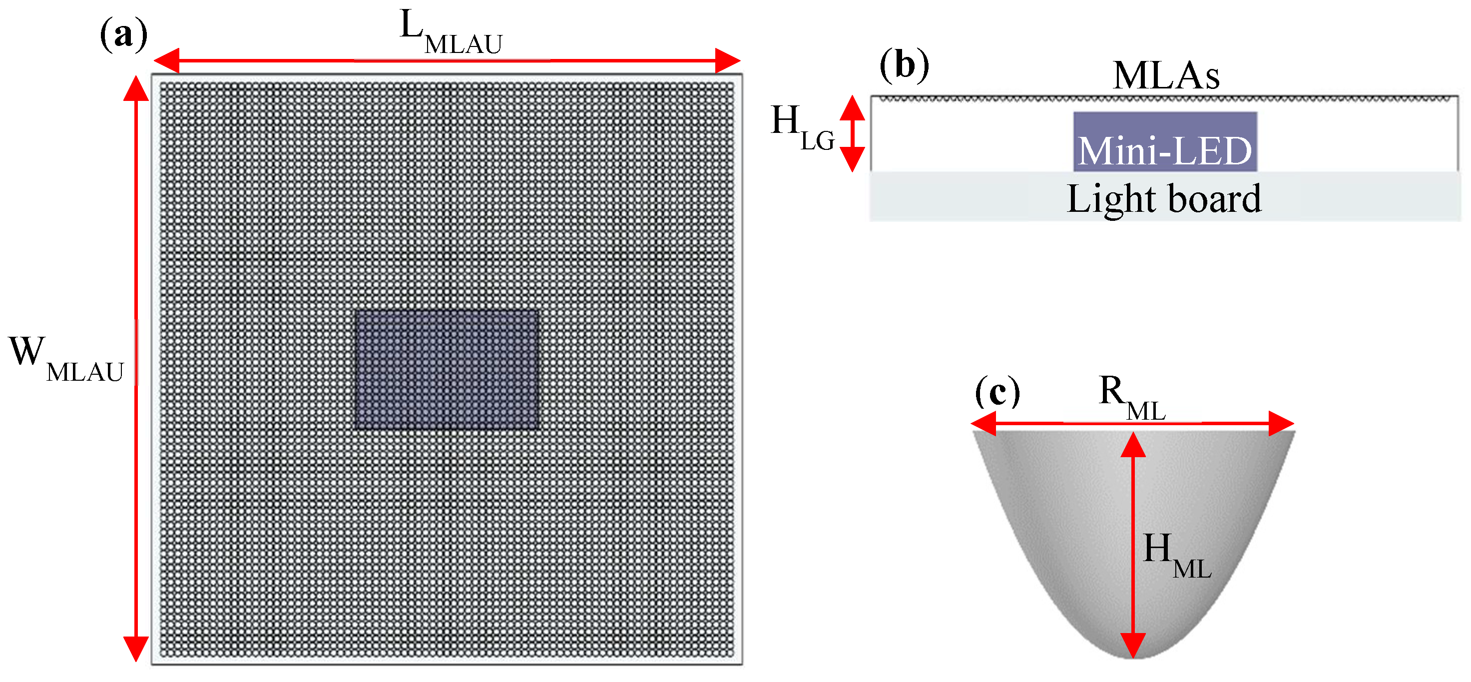
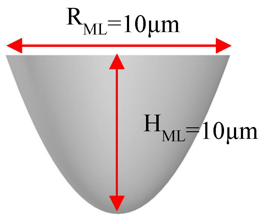
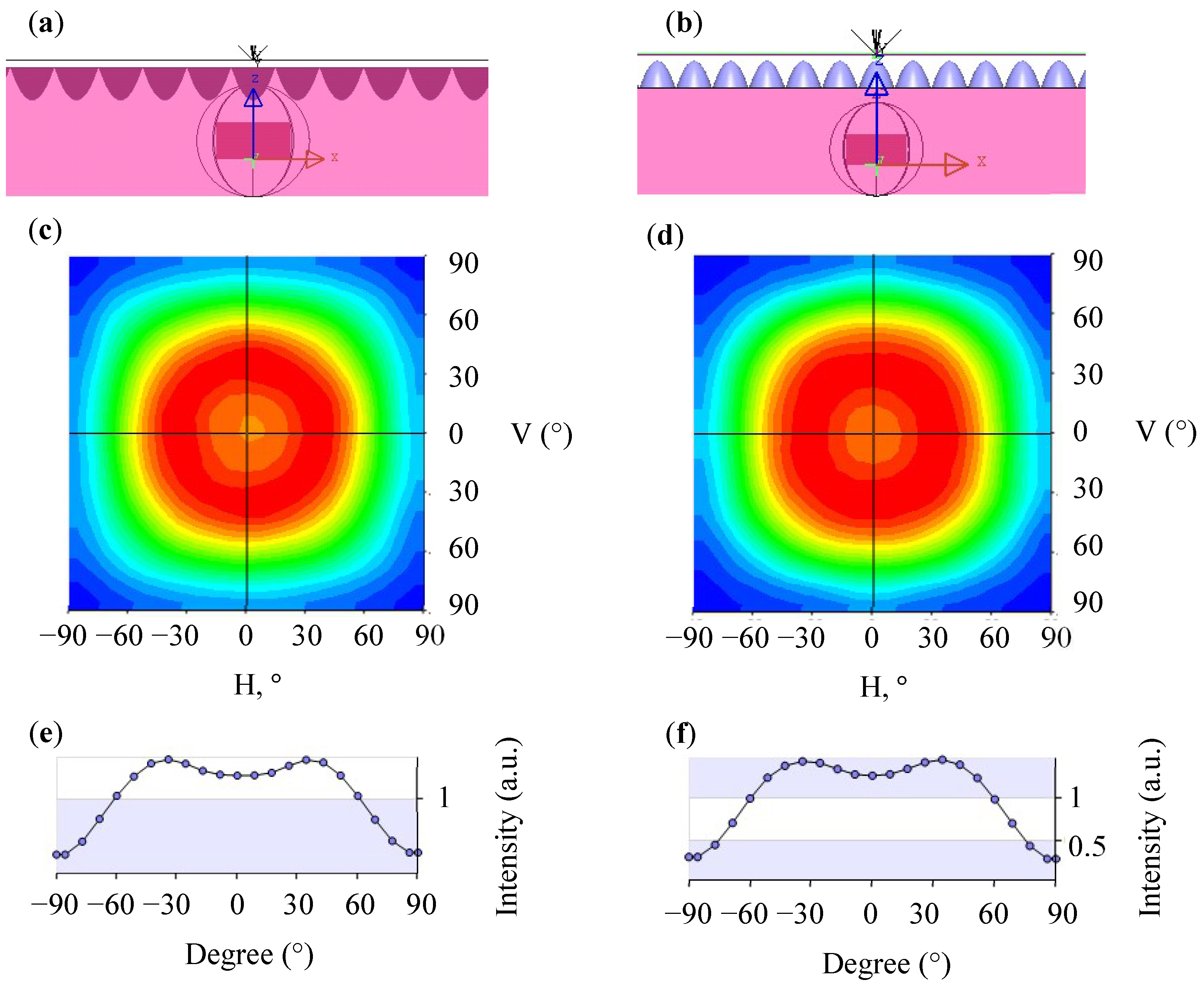
2.2. Model Construction of the MLA Unit
2.3. Simulation and Optimization of the MLA Unit
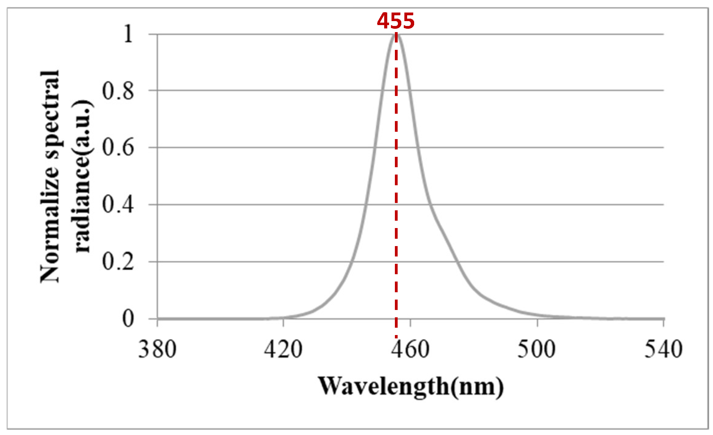
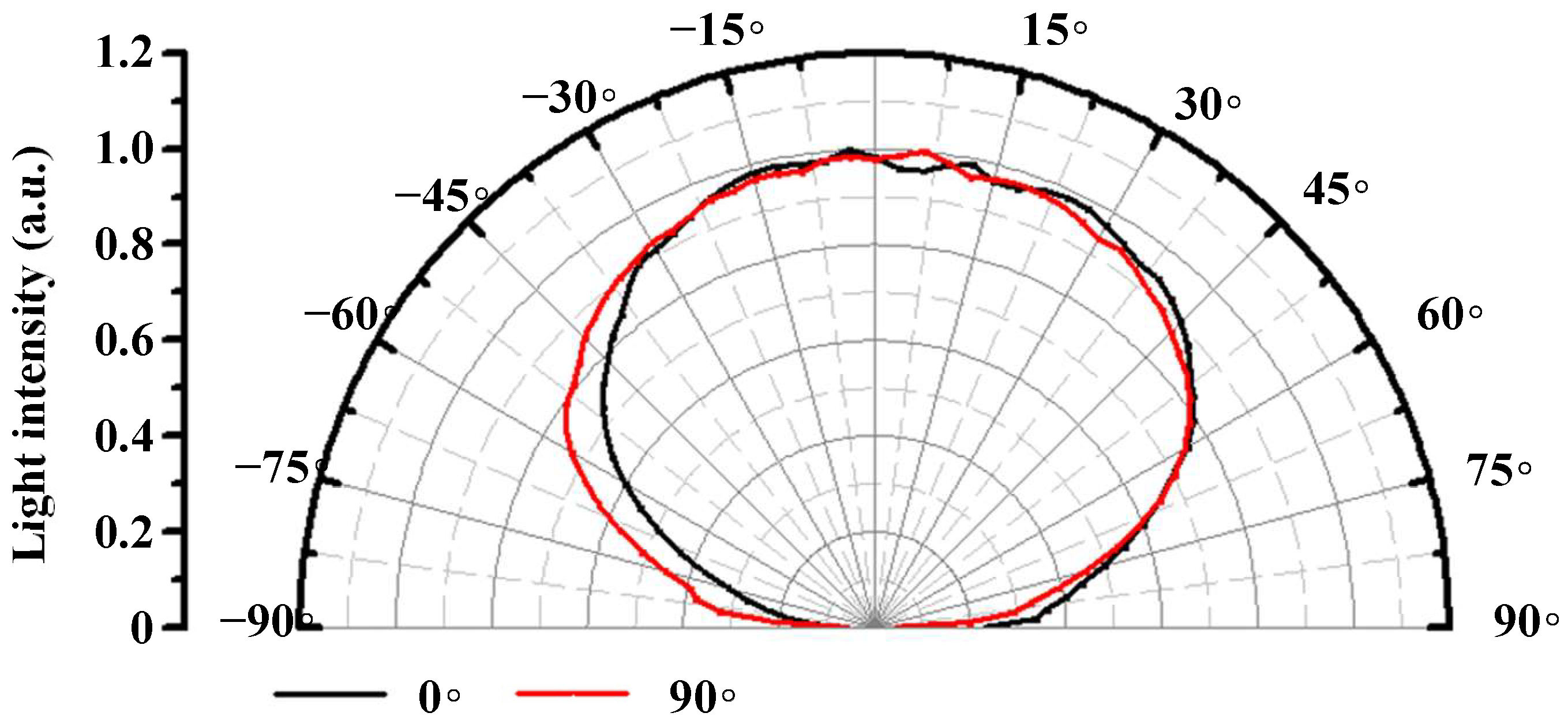
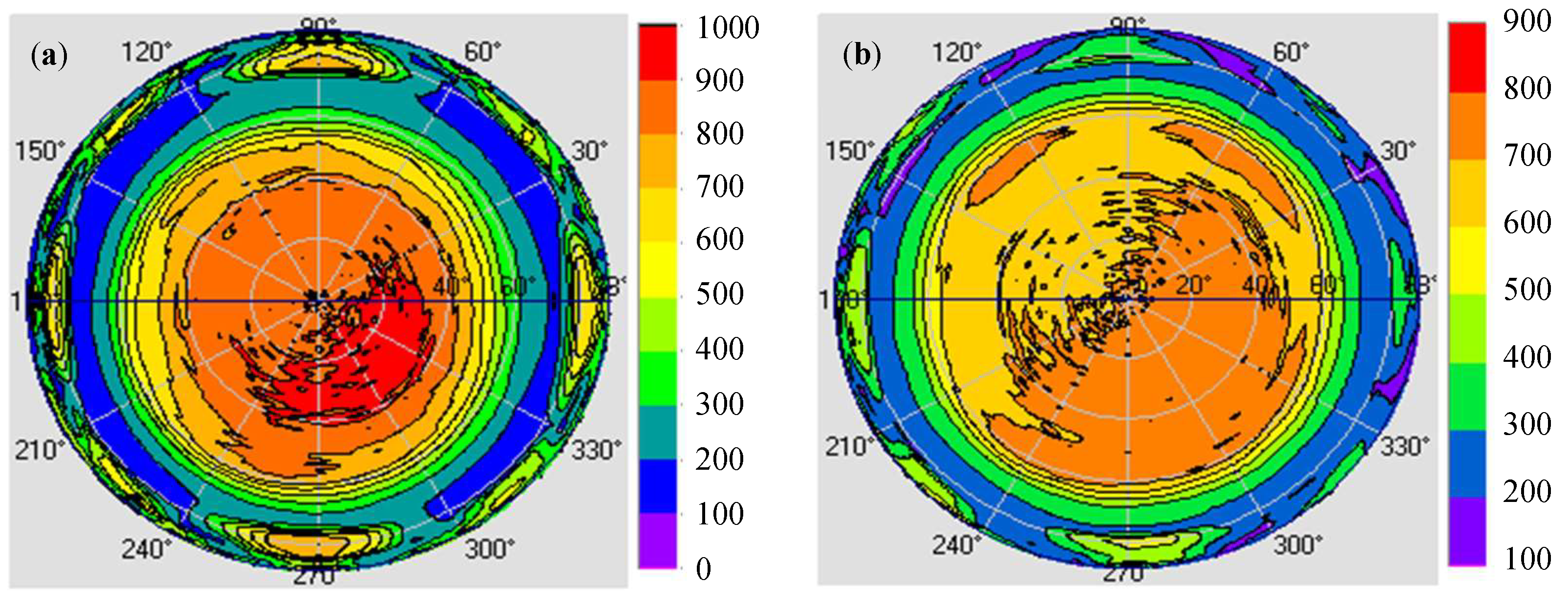
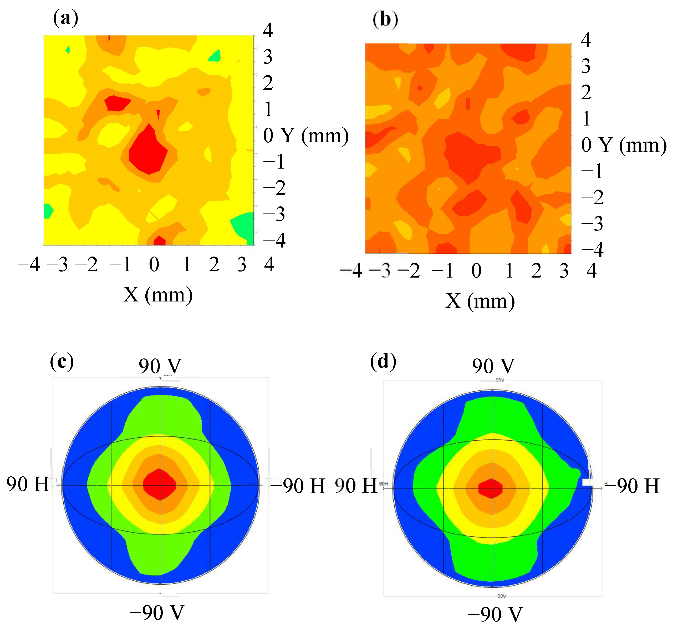
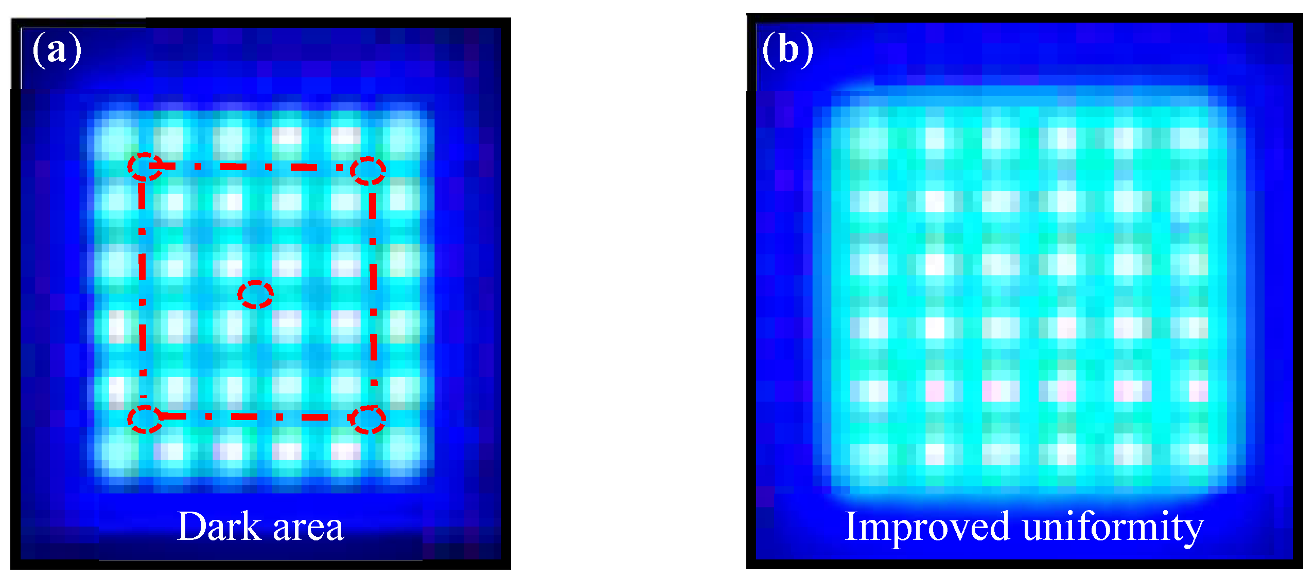
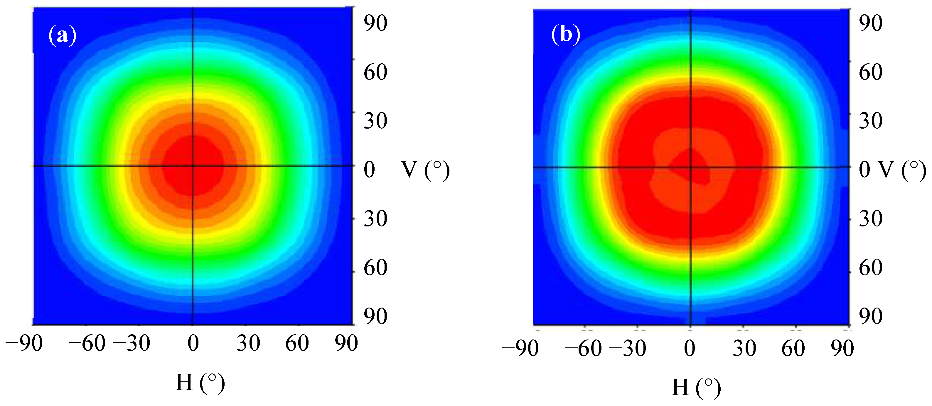
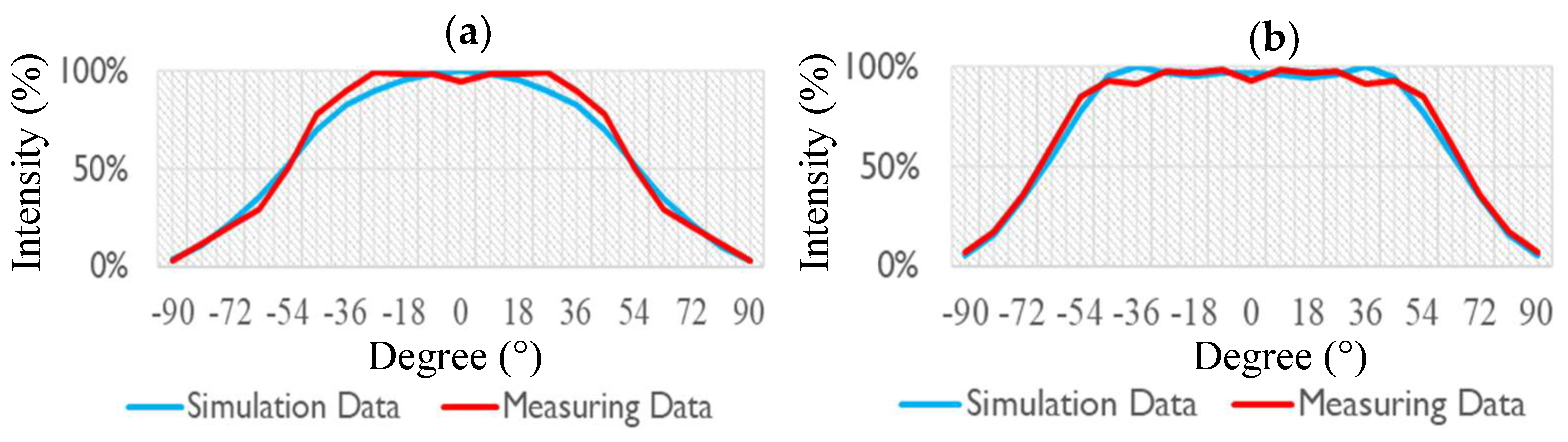
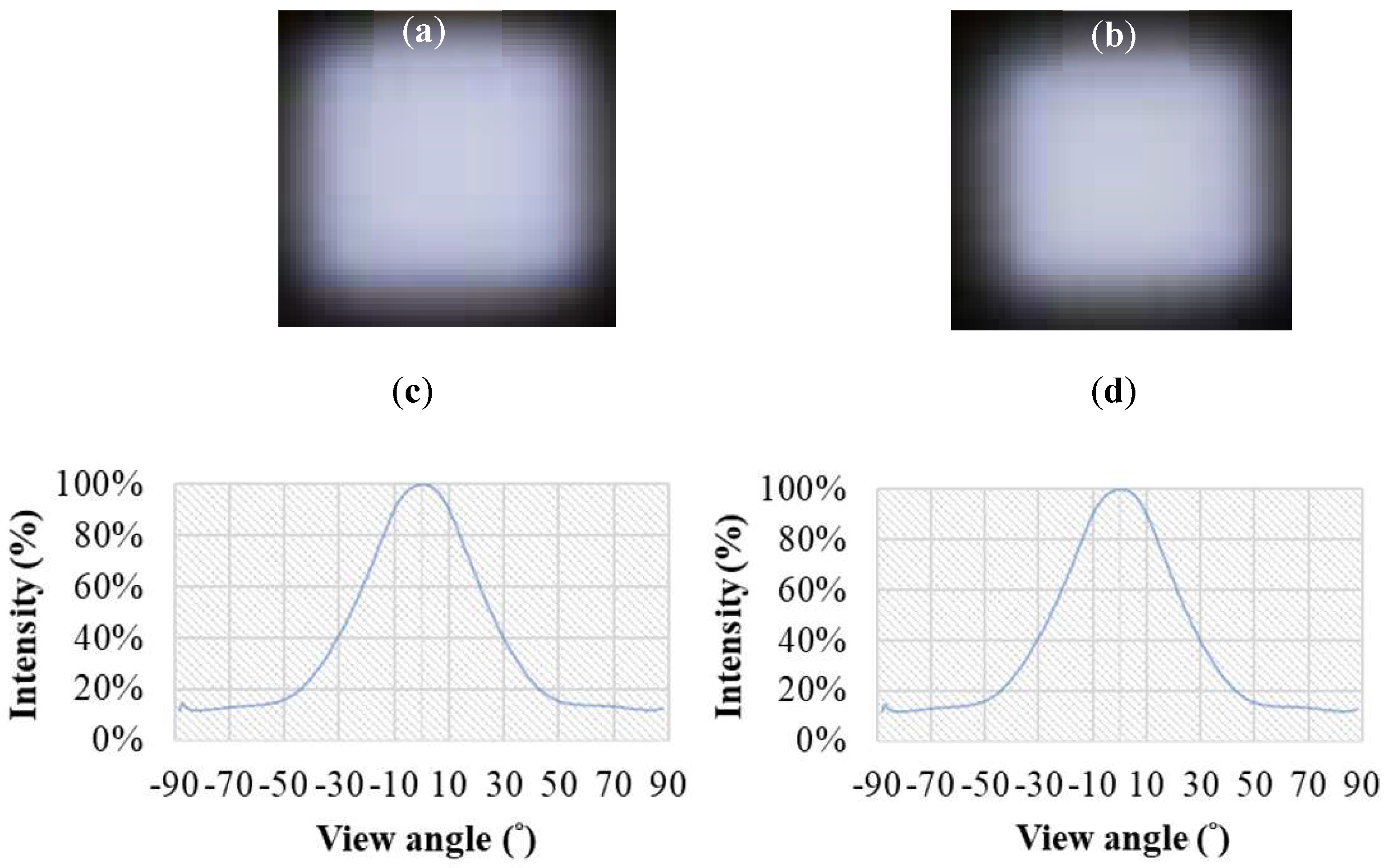
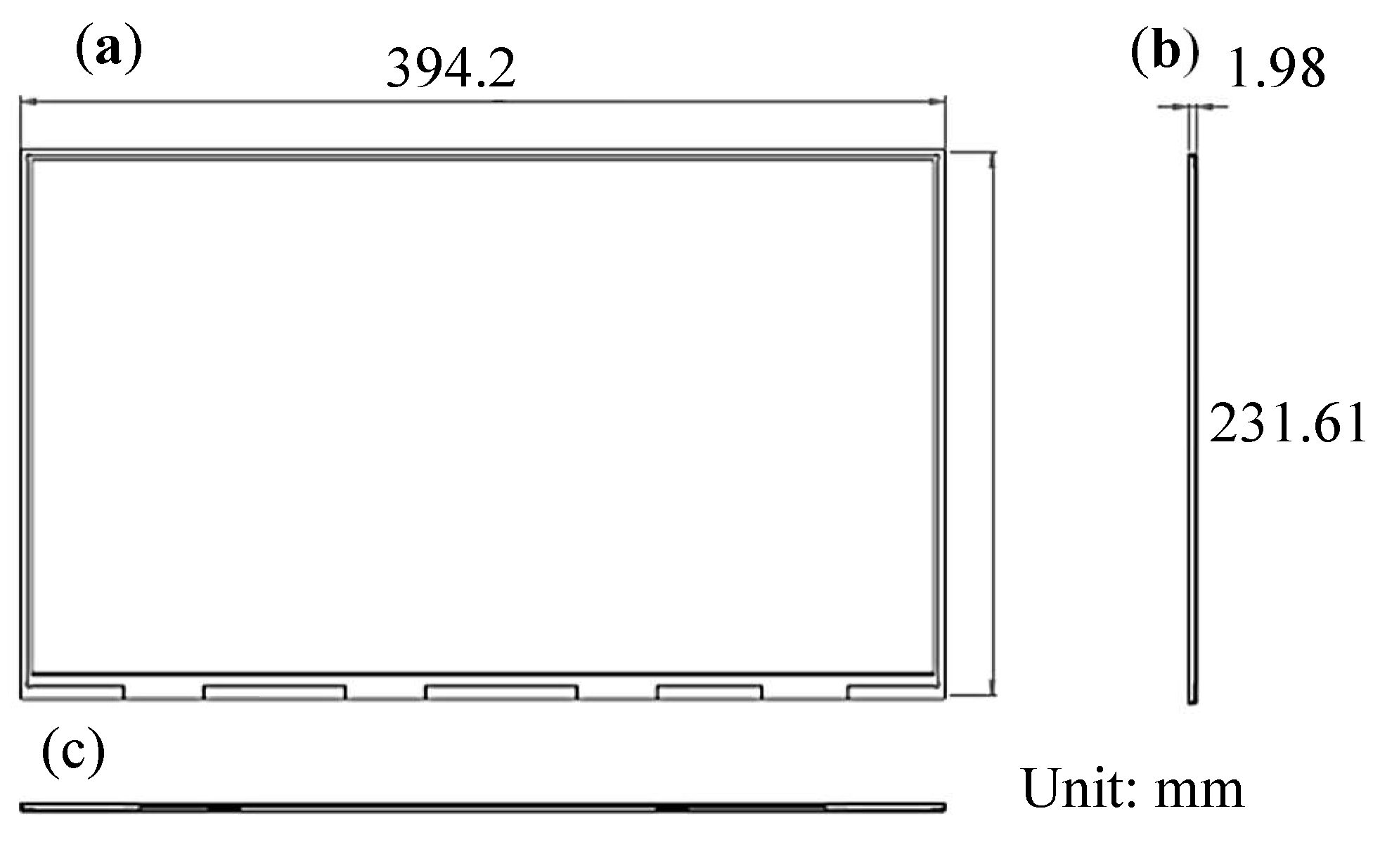
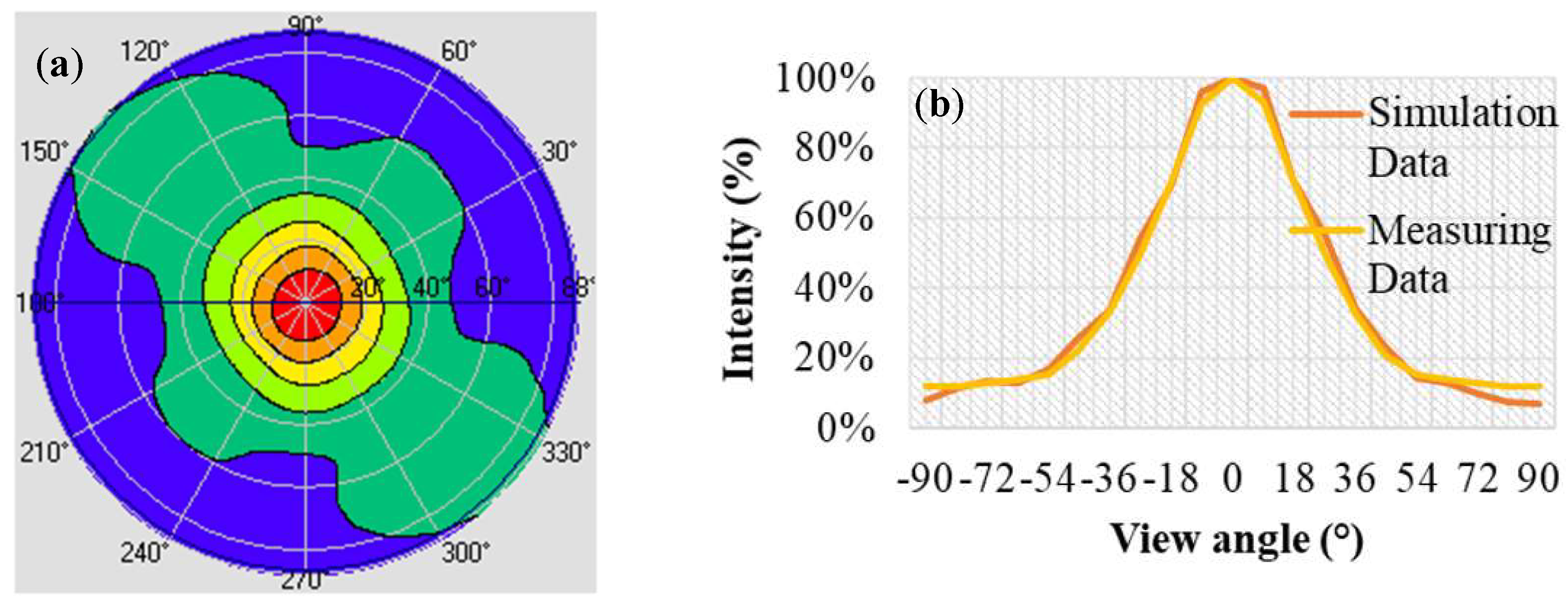
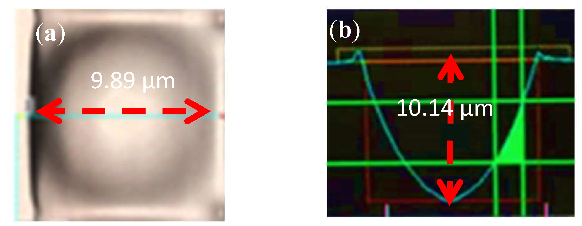
3. Results and Discussion
4. Conclusions
Author Contributions
Funding
Institutional Review Board Statement
Informed Consent Statement
Data Availability Statement
Conflicts of Interest
References
- Hua, J.; Hua, E.; Zhou, F.; Shi, J.; Wang, C.; Duan, H.; Hu, Y.; Qiao, W.; Chen, L. Foveated glasses-free 3D display with ultrawide field of view via a large-scale 2D-metagrating complex. Light. Sci. Appl. 2021, 10, 1–9. [Google Scholar] [CrossRef]
- Park, J.; Choi, J.H.; Kong, K.; Han, J.H.; Park, J.H.; Kim, N.; Lee, E.; Kim, D.; Kim, J.; Chung, D.; et al. Electrically driven mid-submicrometre pixelation of InGaN micro-light-emitting diode displays for augmented-reality glasses. Nat. Photonics 2021, 15, 449–455. [Google Scholar] [CrossRef]
- Xiong, J.; Hsiang, E.-L.; He, Z.; Zhan, T.; Wu, S.-T. Augmented reality and virtual reality displays: Emerging technologies and future perspectives. Light. Sci. Appl. 2021, 10, 1–30. [Google Scholar] [CrossRef]
- Martínez-Corral, M.; Javidi, B. Fundamentals of 3D imaging and displays: A tutorial on integral imaging, light-field, and plenoptic systems. Adv. Opt. Photonics 2018, 10, 512–566. [Google Scholar] [CrossRef] [Green Version]
- Huang, Y.; Hsiang, E.-L.; Deng, M.-Y.; Wu, S.-T. Mini-LED, Micro-LED and OLED displays: Present status and future perspectives. Light. Sci. Appl. 2020, 9, 1–16. [Google Scholar] [CrossRef]
- Li, X.; Zhao, Y.; Fan, F.; Levina, L.; Liu, M.; Quintero-Bermudez, R.; Gong, X.; Na Quan, L.; Fan, J.; Yang, Z.; et al. Bright colloidal quantum dot light-emitting diodes enabled by efficient chlorination. Nat. Photonics 2018, 12, 159–164. [Google Scholar] [CrossRef]
- Chen, H.-W.; Lee, J.-H.; Lin, B.-Y.; Chen, S.; Wu, S.-T. Liquid crystal display and organic light-emitting diode display: Present status and future perspectives. Light. Sci. Appl. 2018, 7, 17168. [Google Scholar] [CrossRef]
- Shen, H.; Gao, Q.; Zhang, Y.; Lin, Y.; Lin, Q.; Li, Z.; Chen, L.; Zeng, Z.; Li, X.; Jia, Y.; et al. Visible quantum dot light-emitting diodes with simultaneous high brightness and efficiency. Nat. Photonics 2019, 13, 192–197. [Google Scholar] [CrossRef]
- Jeon, S.O.; Lee, K.H.; Kim, J.S.; Ihn, S.-G.; Chung, Y.S.; Kim, J.W.; Lee, H.; Kim, S.; Choi, H.; Lee, J.Y. High-efficiency, long-lifetime deep-blue organic light-emitting diodes. Nat. Photonics 2021, 15, 208–215. [Google Scholar] [CrossRef]
- Wei, Y.-C.; Wang, S.F.; Hu, Y.; Liao, L.-S.; Chen, D.-G.; Chang, K.-H.; Wang, C.-W.; Liu, S.-H.; Chan, W.-H.; Liao, J.-L.; et al. Overcoming the energy gap law in near-infrared OLEDs by exciton–vibration decoupling. Nat. Photonics 2020, 14, 570–577. [Google Scholar] [CrossRef]
- Minotto, A.; Bulut, I.; Rapidis, A.G.; Carnicella, G.; Patrini, M.; Lunedei, E.; Anderson, H.L.; Cacialli, F. Towards efficient near-infrared fluorescent organic light-emitting diodes. Light. Sci. Appl. 2021, 10, 1–10. [Google Scholar] [CrossRef]
- Zhou, X.; Qin, G.; Wang, L.; Chen, Z.; Xu, X.; Dong, Y.; Moheghi, A.; Yang, D.-K. Full color waveguide liquid crystal display. Opt. Lett. 2017, 42, 3706–3709. [Google Scholar] [CrossRef]
- Kim, G.; Shih, Y.-C.; Shi, F. Optimal Design of Quantum Dot Color Conversion Film in LCD Backlighting. IEEE J. Sel. Top. Quantum Electron. 2017, 23, 1. [Google Scholar] [CrossRef]
- Chen, E.; Xie, H.; Huang, J.; Miu, H.; Shao, G.; Li, Y.; Guo, T.; Xu, S.; Ye, Y. Flexible/curved backlight module with quantum-dots microstructure array for liquid crystal displays. Opt. Express 2018, 26, 3466–3482. [Google Scholar] [CrossRef]
- Wei, Y.; Xing, G.; Liu, K.; Li, G.; Dang, P.; Liang, S.; Liu, M.; Cheng, Z.; Jin, D.; Lin, J. New strategy for designing orangish-red-emitting phosphor via oxygen-vacancy-induced electronic localization. Light. Sci. Appl. 2019, 8, 1–9. [Google Scholar] [CrossRef]
- Zhao, M.; Liao, H.; Molokeev, M.S.; Zhou, Y.; Zhang, Q.; Liu, Q.; Xia, Z. Emerging ultra-narrow-band cyan-emitting phosphor for white LEDs with enhanced color rendition. Light. Sci. Appl. 2019, 8, 1–9. [Google Scholar] [CrossRef] [Green Version]
- He, S.; Xu, F.; Han, T.; Lu, Z.; Wang, W.; Peng, J.; Du, F.; Yang, F.; Ye, X. A Mn4+-doped oxyfluoride phosphor with remarkable negative thermal quenching and high color stability for warm WLEDs. Chem. Eng. J. 2020, 392, 123657. [Google Scholar] [CrossRef]
- Won, Y.-H.; Cho, O.; Kim, T.; Chung, D.-Y.; Kim, T.; Chung, H.; Jang, H.; Lee, J.; Kim, D.; Jang, E. Highly efficient and stable InP/ZnSe/ZnS quantum dot light-emitting diodes. Nature 2019, 575, 634–638. [Google Scholar] [CrossRef]
- Cao, F.; Wang, S.; Wang, F.; Wu, Q.; Zhao, D.; Yang, X. A layer-by-layer growth strategy for large-size InP/ZnSe/ZnS core–shell quantum dots enabling high-efficiency light-emitting diodes. Chem. Mater. 2018, 30, 8002–8007. [Google Scholar] [CrossRef]
- Zhai, L.; Löbl, M.C.; Nguyen, G.N.; Ritzmann, J.; Javadi, A.; Spinnler, C.; Wieck, A.D.; Ludwig, A.; Warburton, R.J. Low-noise GaAs quantum dots for quantum photonics. Nat. Commun. 2020, 11, 1–8. [Google Scholar] [CrossRef]
- Lin, H.-Y.; Sher, C.-W.; Hsieh, D.-H.; Chen, X.-Y.; Chen, H.-M.P.; Chen, T.-M.; Lau, K.-M.; Chen, C.-H.; Lin, C.-C.; Kuo, H.-C. Optical cross-talk reduction in a quantum-dot-based full-color micro-light-emitting-diode display by a lithographic-fabricated photoresist mold. Photon Res. 2017, 5, 411–416. [Google Scholar] [CrossRef]
- Huang, C.-H.; Chang, S.H.; Liaw, B.-Y.; Liu, C.-Y.; Chou, C.-Y.; Zhou, J.-R.; Lin, C.-C.; Kuo, H.-C.; Song, L.-J.; Li, F.; et al. Research on a Novel GaN-Based Converted Mini-LED Backlight Module via a Spectrum-Decouple System. IEEE Access 2020, 8, 138823–138833. [Google Scholar] [CrossRef]
- He, Z.; Yin, K.; Hsiang, E.-L.; Wu, S.-T. Volumetric light-shaping polymer-dispersed liquid crystal films for mini-LED backlights. Liq. Cryst. 2020, 47, 1458–1463. [Google Scholar] [CrossRef]
- Corbett, B.; Loi, R.; Zhou, W.; Liu, D.; Ma, Z. Transfer print techniques for heterogeneous integration of photonic components. Prog. Quantum Electron. 2017, 52, 1–17. [Google Scholar] [CrossRef]
- Zheng, L.; Guo, Z.; Yan, W.; Lin, Y.; Lu, Y.; Kuo, H.-C.; Chen, Z.; Zhu, L.; Wu, T.; Gao, Y. Research on a Camera-Based Microscopic Imaging System to Inspect the Surface Luminance of the Micro-LED Array. IEEE Access 2018, 6, 51329–51336. [Google Scholar] [CrossRef]
- Chen, S.-W.H.; Shen, C.-C.; Wu, T.; Liao, Z.-Y.; Chen, L.-F.; Zhou, J.-R.; Lee, C.-F.; Lin, C.-H.; Lin, C.-C.; Sher, C.-W.; et al. Full-color monolithic hybrid quantum dot nanoring micro light-emitting diodes with improved efficiency using atomic layer deposition and nonradiative resonant energy transfer. Photon Res. 2019, 7, 416–422. [Google Scholar] [CrossRef]
- Yoon, G.-W.; Bae, S.-W.; Lee, Y.-B.; Yoon, J.-B. Edge-lit LCD backlight unit for 2D local dimming. Opt. Express 2018, 26, 20802–20812. [Google Scholar] [CrossRef]
- Chen, E.; Guo, J.; Jiang, Z.; Shen, Q.; Ye, Y.; Xu, S.; Sun, J.; Yan, Q.; Guo, T. Edge/direct-lit hybrid mini-LED backlight with U-grooved light guiding plates for local dimming. Opt. Express 2021, 29, 12179–12194. [Google Scholar] [CrossRef]
- Zhang, T.; Zeng, Q.; Zhao, X. Optimal local dimming based on an improved greedy algorithm. Appl. Intell. 2020, 50, 4162–4175. [Google Scholar] [CrossRef]
- Duan, L.; Debattista, K.; Lei, Z.; Chalmers, A. Subjective and Objective Evaluation of Local Dimming Algorithms for HDR Images. IEEE Access 2020, 8, 51692–51702. [Google Scholar] [CrossRef]
- Chen, E.; Lin, J.; Yang, T.; Chen, Y.; Zhang, X.; Ye, Y.; Sun, J.; Yan, Q.; Guo, T. Asymmetric quantum-dot pixelation for color-converted white balance. ACS Photonics 2021, 8, 2158–2165. [Google Scholar] [CrossRef]
- Deng, M.-Y.; Hsiang, E.-L.; Yang, Q.; Tsai, C.-L.; Chen, B.-S.; Wu, C.-E.; Lee, M.-H.; Wu, S.-T.; Lin, C.-L. Reducing power consumption of active-matrix mini-LED backlit LCDs by driving circuit. IEEE Trans. Electron Devices 2021, 68, 2347–2354. [Google Scholar] [CrossRef]
- Hsiang, E.-L.; Yang, Q.; He, Z.; Zou, J.; Wu, S.-T. Halo effect in high-dynamic-range mini-LED backlit LCDs. Opt. Express 2020, 28, 36822–36837. [Google Scholar] [CrossRef]
- Tan, G.; Huang, Y.; Li, M.-C.; Lee, S.-L.; Wu, S.-T. High dynamic range liquid crystal displays with a mini-LED backlight. Opt. Express 2018, 26, 16572–16584. [Google Scholar] [CrossRef] [Green Version]
- Guo, W.; Chen, N.; Lu, H.; Su, C.; Lin, Y.; Chen, G.; Lu, Y.; Zheng, L.; Peng, Z.; Kuo, H.-C.; et al. The Impact of luminous properties of red, green, and blue mini-LEDs on the color gamut. IEEE Trans. Electron Devices 2019, 66, 2263–2268. [Google Scholar] [CrossRef]
- Huang, C.-H.; Kang, C.-Y.; Chang, S.-H.; Lin, C.-H.; Lin, C.-Y.; Wu, T.; Sher, C.-W.; Lin, C.-C.; Lee, P.-T.; Kuo, H.-C. Ultra-high light extraction efficiency and ultra-thin mini-LED solution by freeform surface chip scale package array. Crystals 2019, 9, 202. [Google Scholar] [CrossRef] [Green Version]
- Xu, L.; Ming, C.C.; Li, Y.; Fan, K.; Zhang, M.; Sun, H.; Guo, Z. Uniform illumination realized by large viewing angle of gallium nitride-based mini-LED chip with translucent sublayer pairs. IEEE Access 2021, 9, 74713–74718. [Google Scholar] [CrossRef]
- Tang, X.; Han, L.; Ma, Z.; Deng, Z.; Jiang, Y.; Wang, W.; Chen, H.; Du, C.; Jia, H. Enhanced light extraction from AlGaInP-based red light-emitting diodes with photonic crystals. Opt. Express 2021, 29, 5993–5999. [Google Scholar] [CrossRef]
- Jiao, Q.; Chen, Z.; Feng, Y.; Li, S.; Jiang, S.; Li, J.; Chen, Y.; Yu, T.; Kang, X.; Shen, B.; et al. The effects of nanocavity and photonic crystal in InGaN/GaN nanorod LED arrays. Nanoscale Res. Lett. 2016, 11, 340. [Google Scholar] [CrossRef] [Green Version]
- Ye, Z.-T.; Ho, W.-T.; Chen, C.-H. Highly reflective thin-film optimization for full-angle micro-LEDs. Nanoscale Res. Lett. 2021, 16, 1–12. [Google Scholar] [CrossRef]
- Zhu, Z.-M.; Yuan, J.; Sun, X.; Peng, B.; Xu, X.; Liu, Q.-X. LED diffused transmission freeform surface design for uniform illumination. J. Opt. 2019, 48, 232–239. [Google Scholar] [CrossRef] [Green Version]
- Sun, X.; Kong, L.; Qi, L.; Xu, M. Design and analysis of a total-internal-reflection (TIR) structure based on ray-mapping method for tailored illumination. IEEE Access 2020, 8, 45887–45894. [Google Scholar] [CrossRef]
- Ye, Z.-T.; Pai, Y.-M.; Chen, C.-H.; Kuo, H.-C.; Chen, L.-C. A light guide plate that uses asymmetric intensity distribution of mini-LEDs for the planar illuminator. Crystals 2019, 9, 141. [Google Scholar] [CrossRef] [Green Version]
- Ye, Z.T.; Chen, C.L.; Chen, L.-C.; Tien, C.H.; Nguyen, H.T.; Wang, H.-C. Hollow light guide module involving mini light-emitting diodes for asymmetric luminous planar illuminators. Energies 2019, 12, 2755. [Google Scholar] [CrossRef] [Green Version]
- Lu, B.; Wang, Y.; Hyun, B.-R.; Kuo, H.-C.; Liu, Z. Color difference and thermal stability of flexible transparent InGaN/GaN multiple quantum wells mini-LED arrays. IEEE Electron Device Lett. 2020, 41, 1040–1043. [Google Scholar] [CrossRef]
- Chen, L.-C.; Tien, C.-H.; Chen, D.-F.; Ye, Z.-T.; Kuo, H.-C. High-uniformity planar mini-chip-scale packaged LEDs with quantum dot converter for white light source. Nanoscale Res. Lett. 2019, 14, 1–10. [Google Scholar] [CrossRef] [Green Version]
- Feng, Q.; Xiao, H.; Yang, L.; Zhu, B.; Yuan, Y.; Wang, Z.; Lv, G. Ultrathin miniLED backlight system using optical film with microstructures. Appl. Opt. 2021, 60, 9497. [Google Scholar] [CrossRef]
- Ye, Z.T.; Cheng, Y.H.; Liu, K.H.; Yang, K.S. Mini-LEDs with diffuse reflection cavity arrays and quantum dot film for thin, large-area, high-luminance flat light source. Nanomaterials 2021, 11, 2395. [Google Scholar] [CrossRef]
- Kikuchi, S.; Shibata, Y.; Ishinabe, T.; Fujikake, H. Thin mini-LED backlight using reflective mirror dots with high luminance uniformity for mobile LCDs. Opt. Express 2021, 29, 26724. [Google Scholar] [CrossRef]


| Brightness enhancement film | Polyethylene terephthalate with a refractive index of 1.56 and a vertex angle of 90° |
| Light guide layer | Poly(methyl methacrylate) with refractive index of 1.5 |
| Light board | Lambertian diffusion surface with reflectance of 90% |
| Light source settings | Output power: 1 W Center wavelength: 450 nm Number of rays: 50 million |
| Microstructure | Average Full Width at Half Maximum (Degree) |
|---|---|
| Without MLA structure | 117.57° |
| With concave PSMLA structure | 141.82° |
| With convex PSMLA structure | 141.45° |
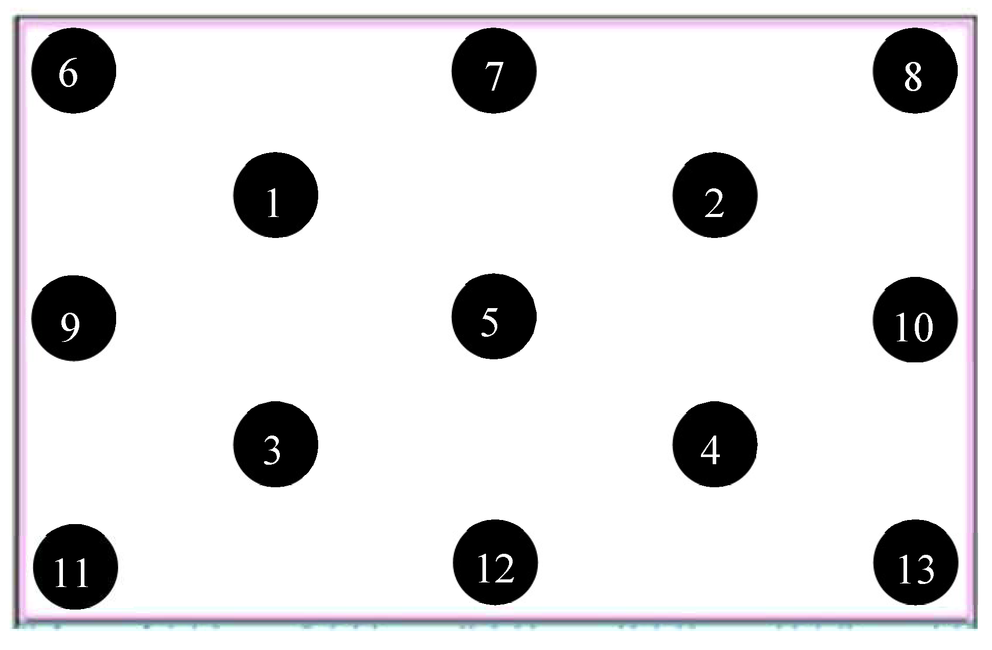
| Measurement Point | Luminance (nits) |
|---|---|
| P1 | 18,641 |
| P2 | 18,825 |
| P3 | 17,785 |
| P4 | 18,160 |
| P5 | 18,852 |
| P6 | 17,234 |
| P7 | 17,251 |
| P8 | 17,079 |
| P9 | 17,303 |
| P10 | 17,854 |
| P11 | 16,818 |
| P12 | 16,546 |
| P13 | 16,115 |
| Average luminance | 17,574 |
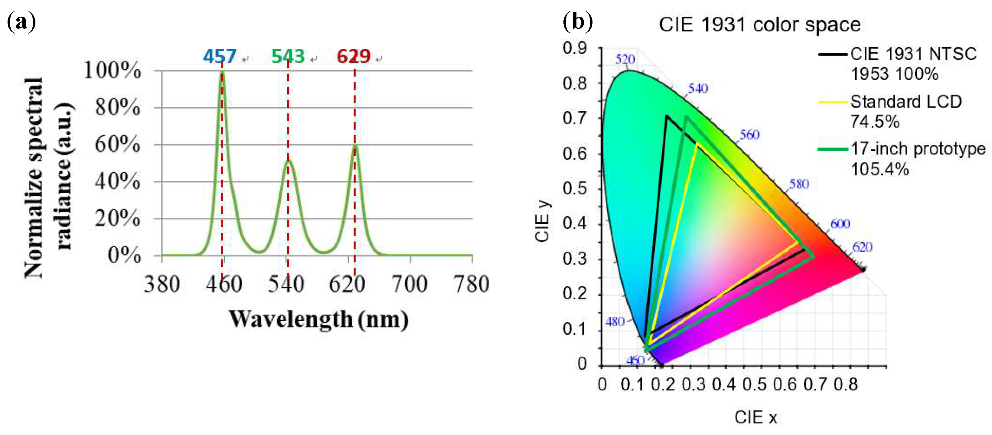
| Color Gamut | Vertex Coordinates (x, y) |
|---|---|
| R | (0.693, 0.307) |
| G | (0.275, 0.708) |
| B | (0.142, 0.038) |
Publisher’s Note: MDPI stays neutral with regard to jurisdictional claims in published maps and institutional affiliations. |
© 2022 by the authors. Licensee MDPI, Basel, Switzerland. This article is an open access article distributed under the terms and conditions of the Creative Commons Attribution (CC BY) license (https://creativecommons.org/licenses/by/4.0/).
Share and Cite
Chen, Y.L.; Ye, Z.T.; Lai, W.; Chiu, C.C.; Lin, K.W.; Han, P. Application of Mini-LEDs with Microlens Arrays and Quantum Dot Film as Extra-Thin, Large-Area, and High-Luminance Backlight. Nanomaterials 2022, 12, 1032. https://doi.org/10.3390/nano12061032
Chen YL, Ye ZT, Lai W, Chiu CC, Lin KW, Han P. Application of Mini-LEDs with Microlens Arrays and Quantum Dot Film as Extra-Thin, Large-Area, and High-Luminance Backlight. Nanomaterials. 2022; 12(6):1032. https://doi.org/10.3390/nano12061032
Chicago/Turabian StyleChen, Yen Lung, Zhi Ting Ye, Wei Lai, Chang Che Chiu, Kuo Wei Lin, and Pin Han. 2022. "Application of Mini-LEDs with Microlens Arrays and Quantum Dot Film as Extra-Thin, Large-Area, and High-Luminance Backlight" Nanomaterials 12, no. 6: 1032. https://doi.org/10.3390/nano12061032