
Metamaterials and Metasurfaces: A Review from the Perspectives of Materials, Mechanisms and Advanced Metadevices


Abstract
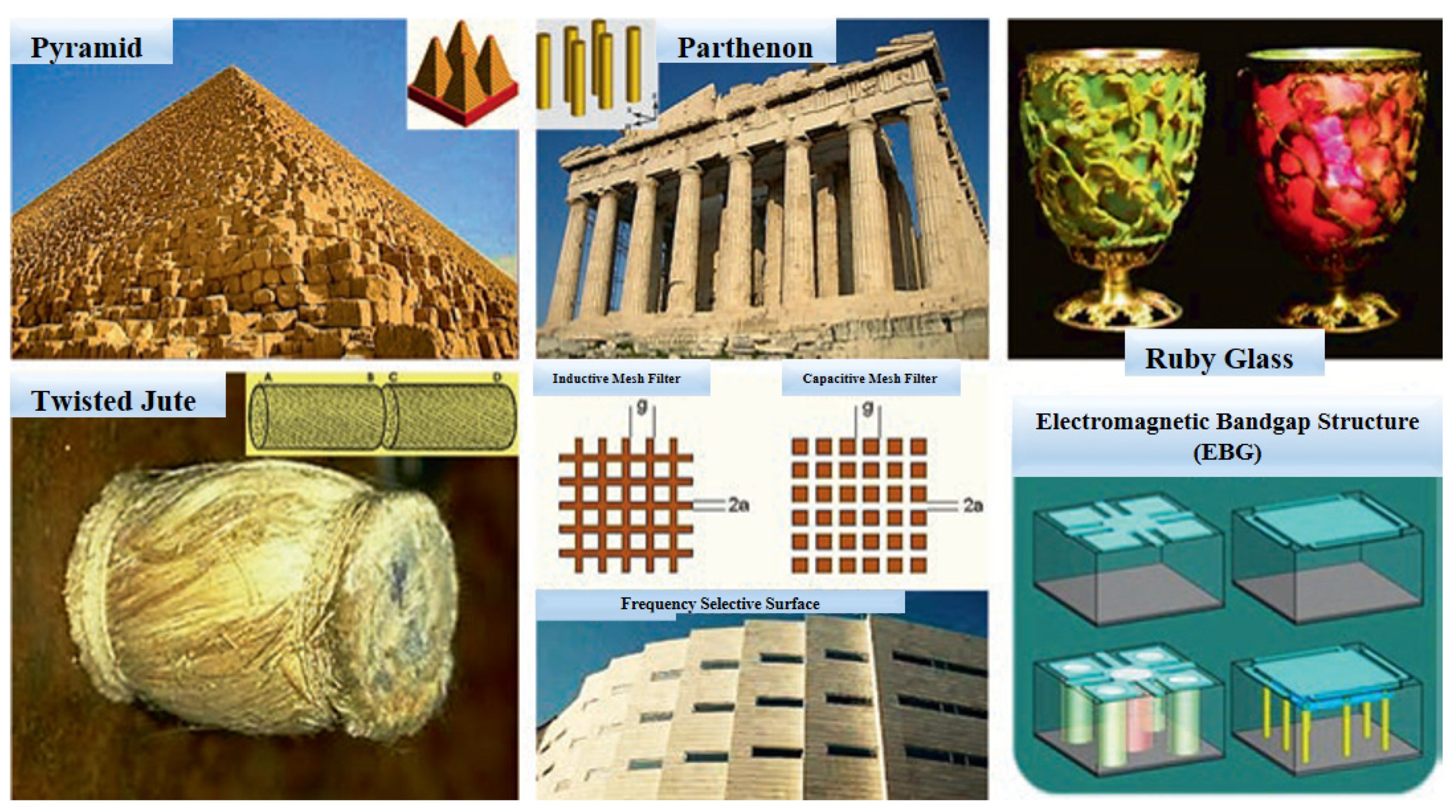
:1. Introduction to Metamaterials
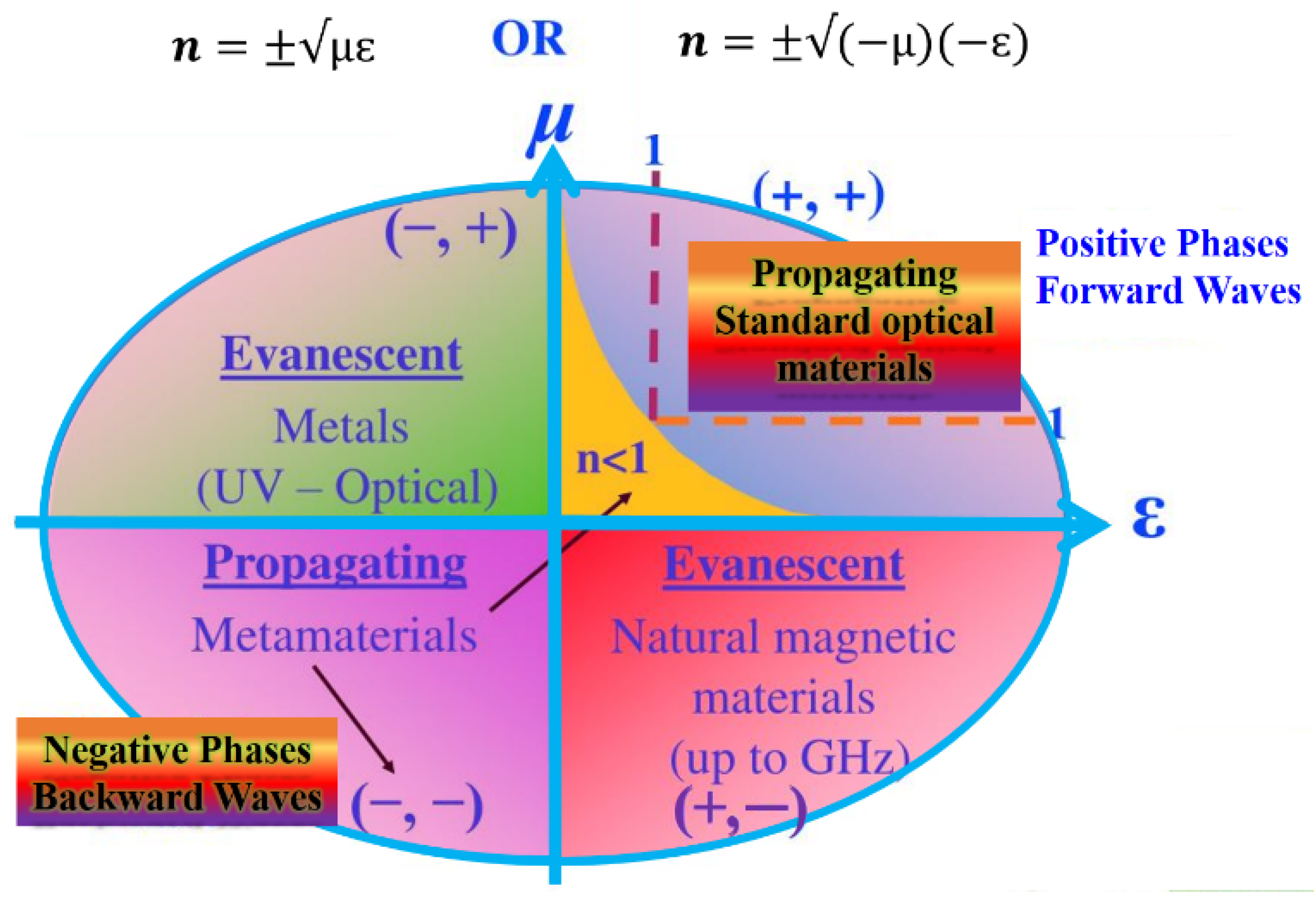
2. Classification of Metamaterials According to Their Physical Properties
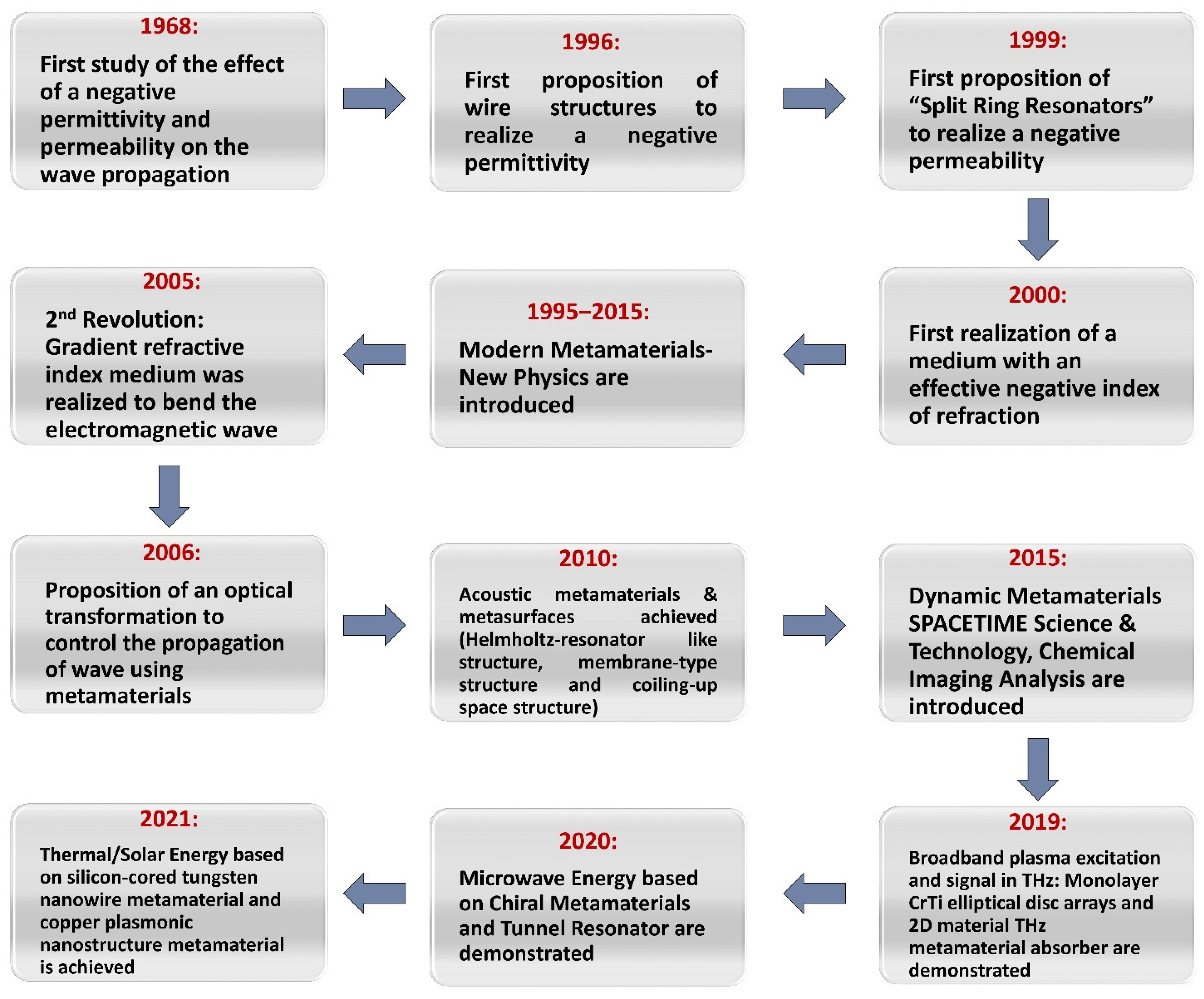
3. Evolution of Metamaterials
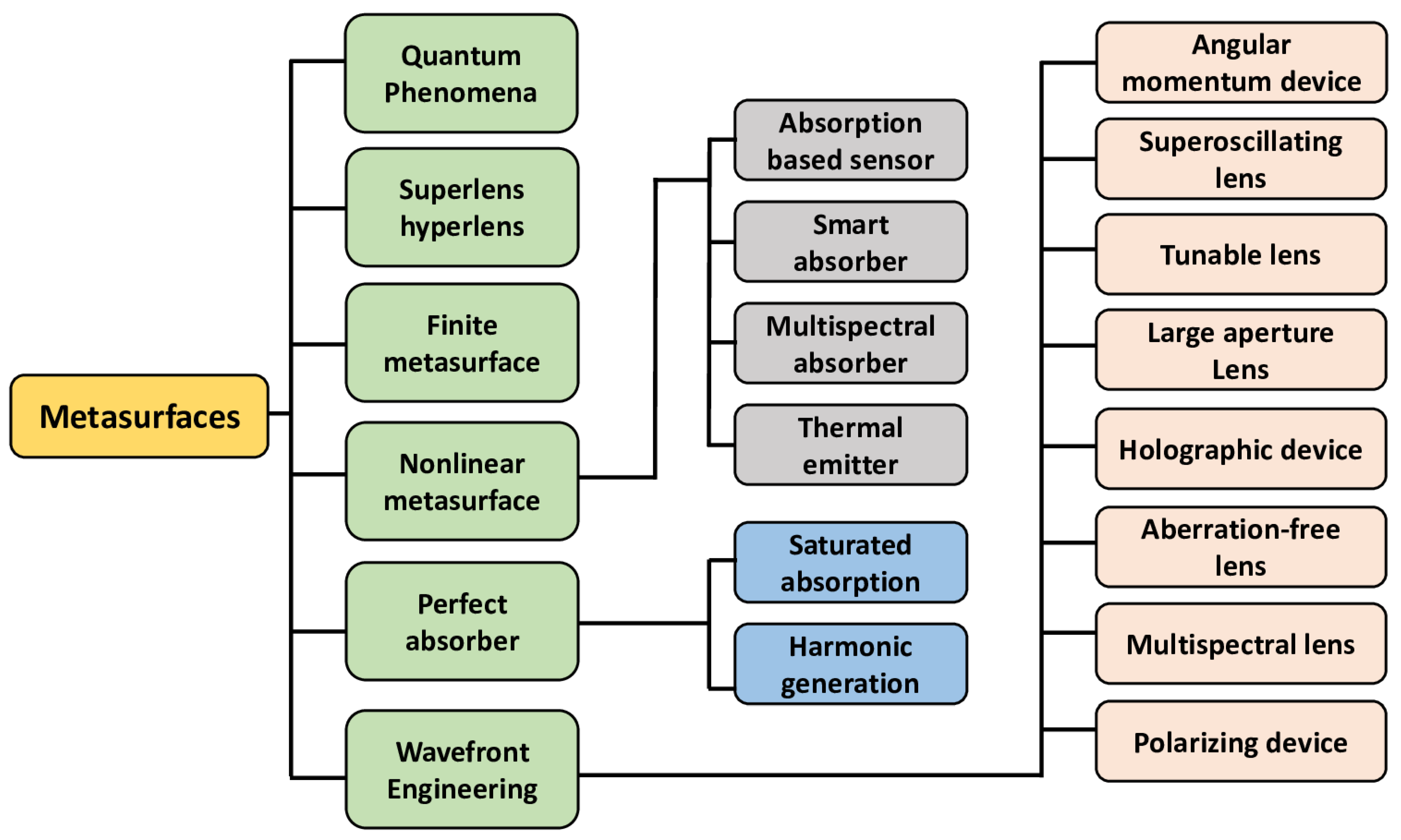
Metasurfaces
4. Metamaterial Fabrication Techniques
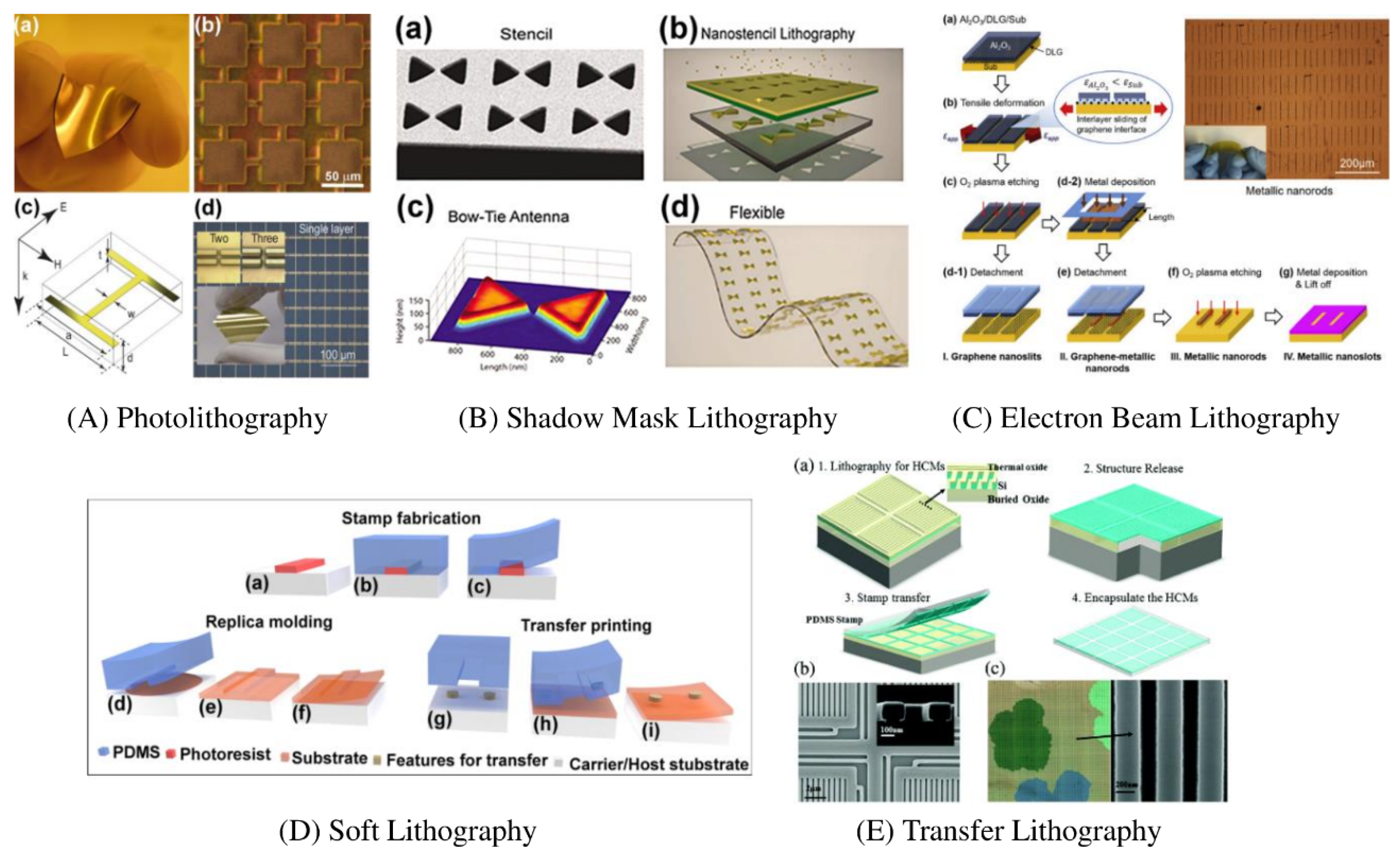
4.1. Photolithography
4.2. Shadow Mask Lithography
4.3. Soft Lithography
4.4. Electron Beam Lithography
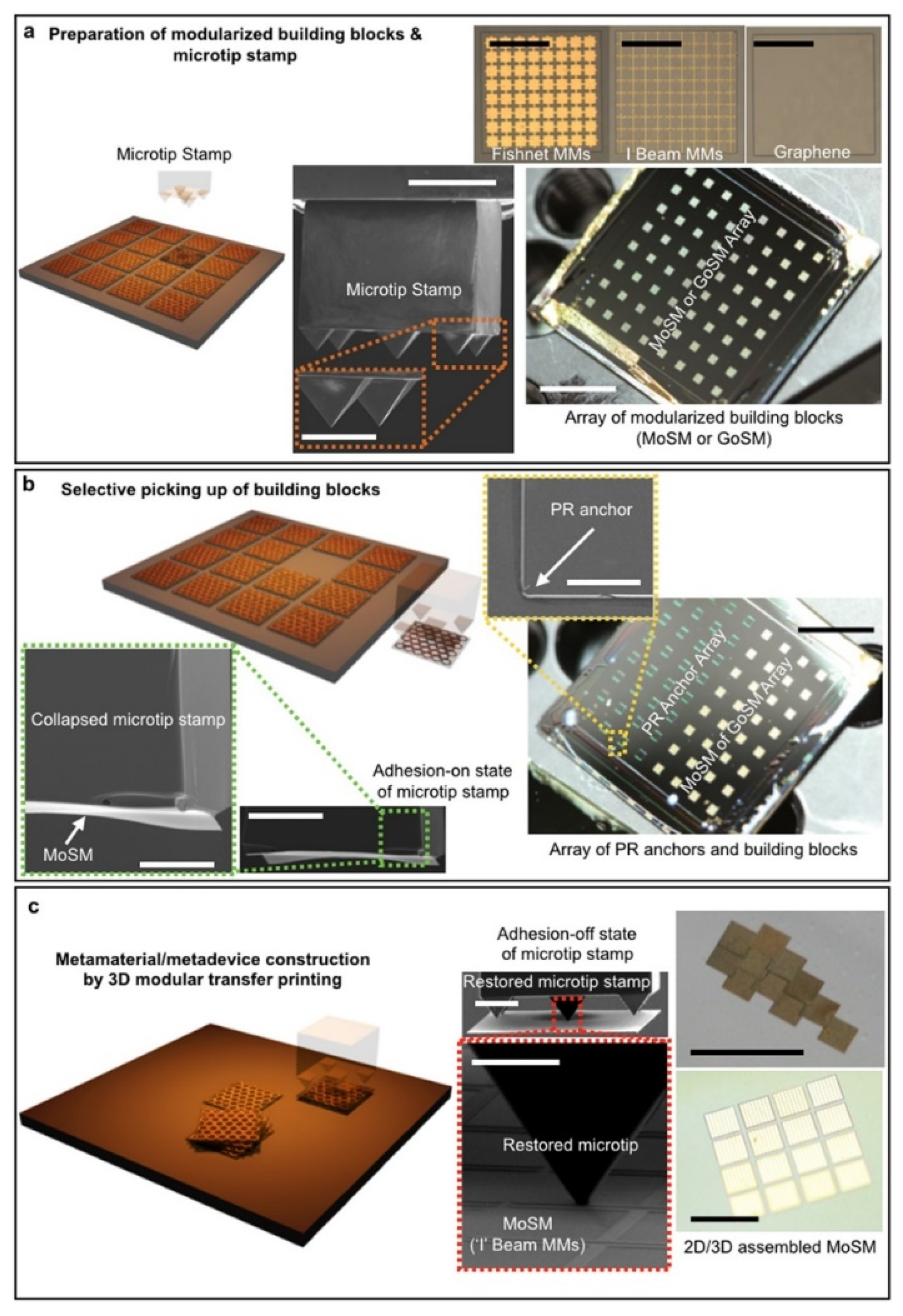
4.5. Three-Dimensional Metamaterial Fabrication Techniques
5. Emerging Functional Metadevices
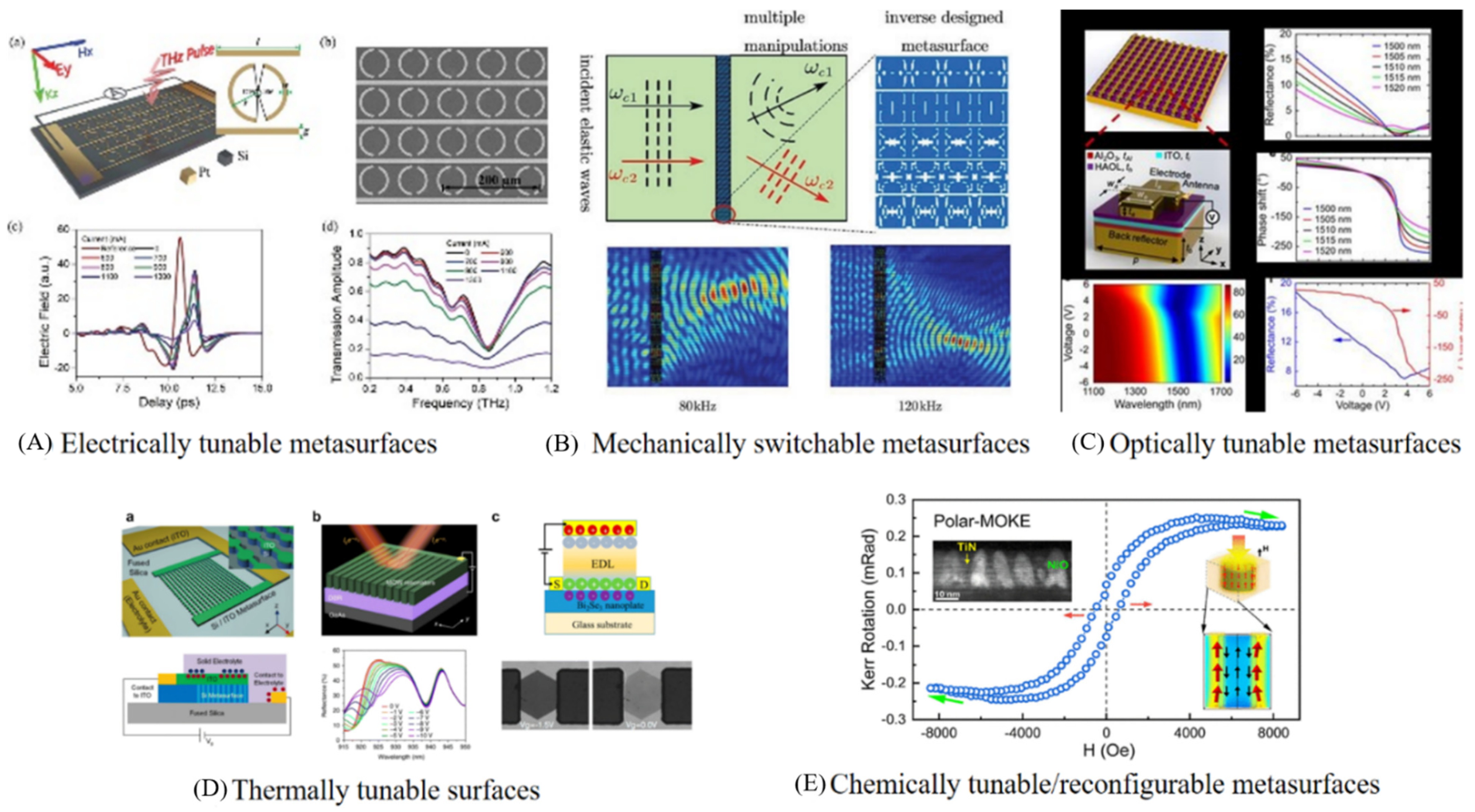
5.1. Tunable and Reconfigurable Metadevices
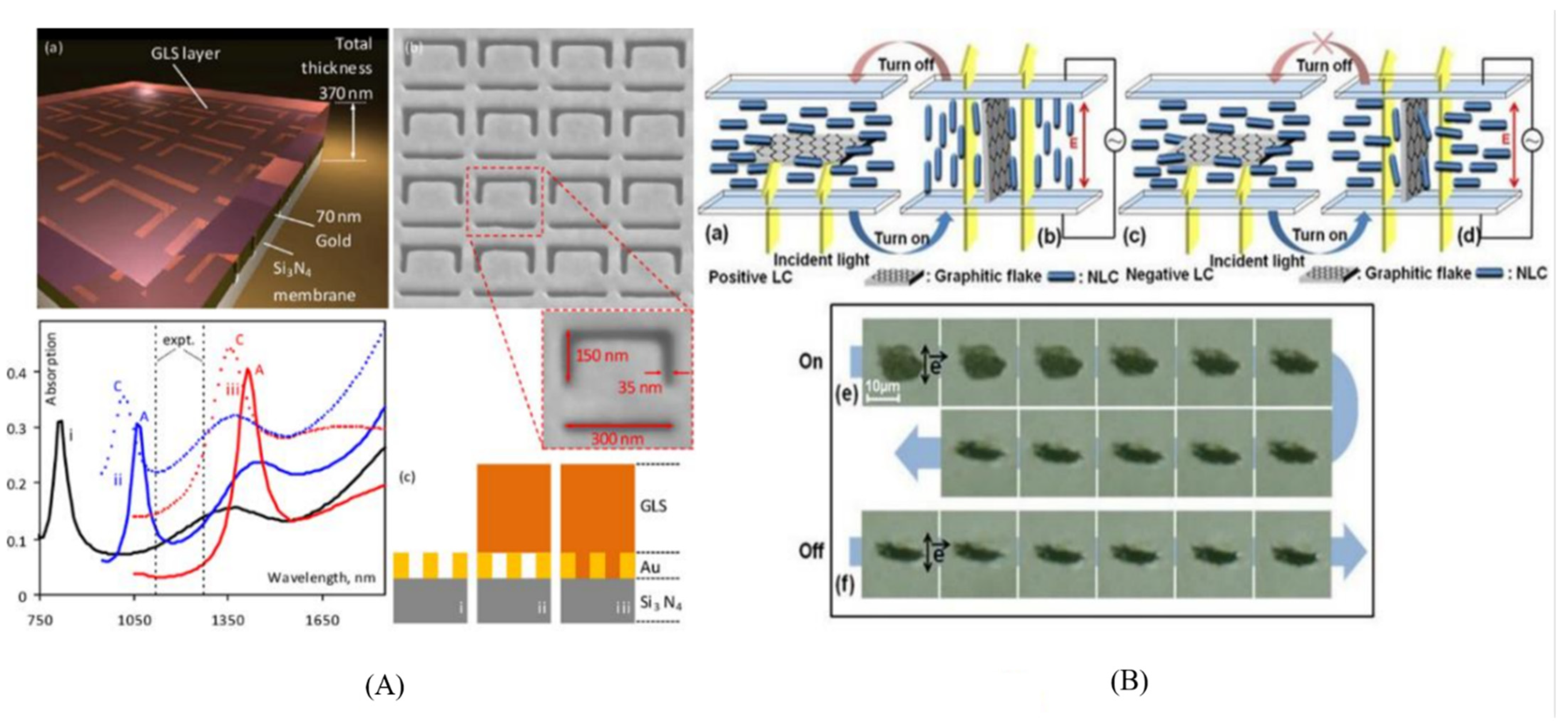
5.2. Electro-Optical Metadevices
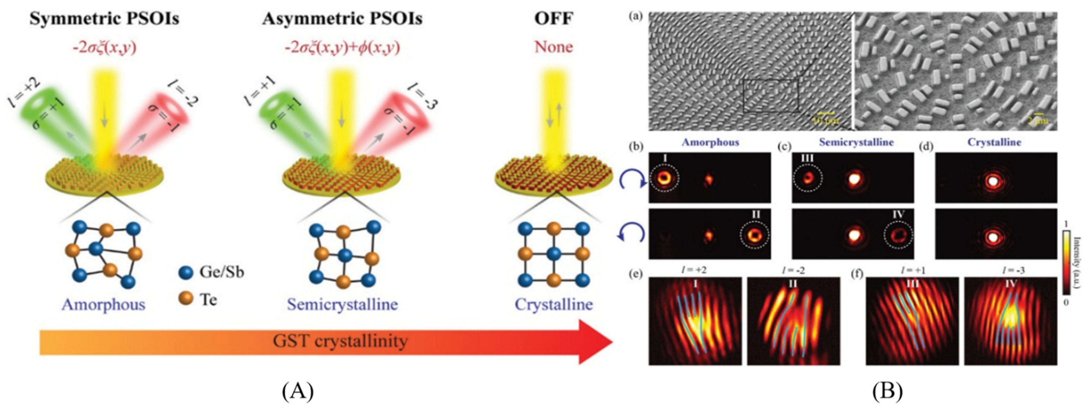
5.3. Phase-Change Metadevices
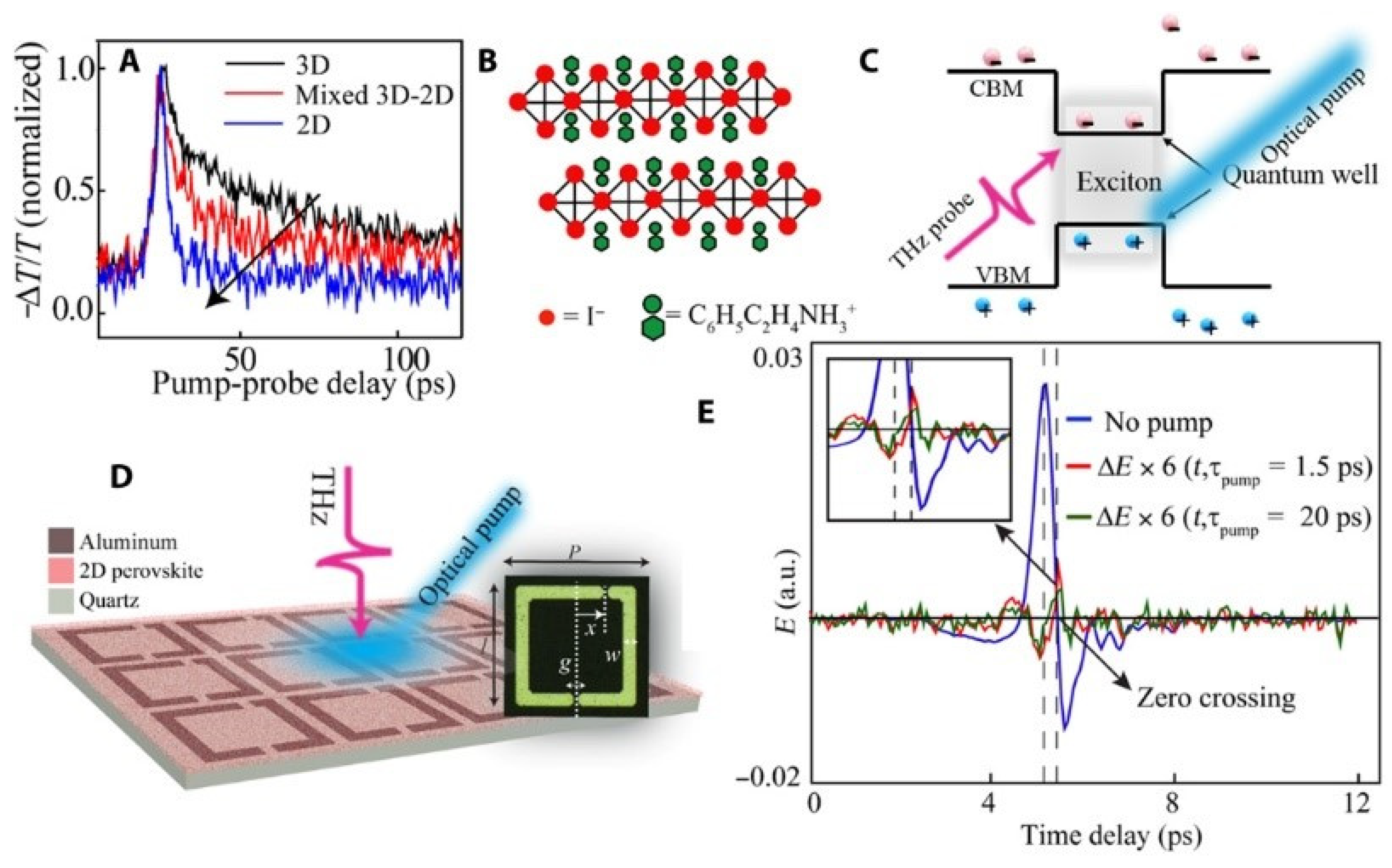
5.4. Ultrafast Photonic Metadevices
5.5. Nonlinear Metadevices with Varactors
6. Photonic Band Gap
Photonic Band Gap Materials to Enhance Solar Cell Efficiency
7. Solar Cell Efficiency Enhancement and Negative Refractive Index Materials
8. Metamaterials and Metasurfaces: Glimpses of New Trends
8.1. Terahertz Metamaterials
8.2. Chiral Metamaterials
8.3. Acoustic Metasurfaces
8.4. Bianisotropic Metasurfaces
8.5. Quantum Photonics Metasurfaces
8.6. Liquid Crystal-Based Metamaterials
8.7. Non-Hermitian Photonics and Metamaterials/Metasurfaces
8.8. Metamaterials-Based Coherent Perfect Absorber
9. Summary
Author Contributions
Funding
Conflicts of Interest
References
- Veselago, V.G. The electrodynamics of substances with simultaneously negative values of ε and μ. Sov. Phys. Uspekhi 1968, 10, 509–514. [Google Scholar] [CrossRef]
- Boyarsky, M.; Sleasman, T.; Pulido-Mancera, L.; Fromenteze, T.; Pedross-Engel, A.; Watts, C.; Imani, M.; Reynolds, M.; Smith, D. Synthetic aperture radar with dynamic metasurface antennas: A conceptual development. J. Opt. Soc. Am. A Opt. Image Sci. Vis. 2017, 34, A22–A36. [Google Scholar] [CrossRef] [PubMed]
- Hsu, H.-T.; Chang, T.-W.; Yang, T.-J.; Chu, B.-H.; Wu, C.-J. Analysis of Wave Properties in Photonic Crystal Narrowband Filters with Left-Handed Defect. J. Electromagn. Waves Appl. 2010, 24, 2285–2298. [Google Scholar] [CrossRef]
- Lou, J.; Liang, J.; Yu, Y.; Ma, H.; Yang, R.; Fan, Y.; Wang, G.; Cai, T. Silicon-Based Terahertz Meta-Devices for Electrical Modulation of Fano Resonance and Transmission Amplitude. Adv. Opt. Mater. 2020, 18, 2000449. [Google Scholar] [CrossRef]
- Kumar, A.; Solanki, A.; Manjappa, M.; Ramesh, S.; Srivastava, Y.K.; Agarwal, P.; Sum, T.C.; Singh, R. Excitons in 2D perovskites for ultrafast terahertz photonic devices. Sci. Adv. 2020, 6, eaax8821. [Google Scholar] [CrossRef] [Green Version]
- Walser, R. Metamaterials: What are they? What are they good for? Acta Obs. Gynecol Scand. 2018, 97, 388–393. [Google Scholar] [CrossRef]
- Gupta, T.K.; Singh, B.P.; Singh, V.N.; Teotia, S.; Singh, A.P.; Elizabeth, I.; Dhakate, S.R.; Dhawan, S.K.; Mathur, R.B. MnO2 decorated graphene nanoribbons with superior permittivity and excellent microwave shielding properties. J. Mater. Chem. A 2014, 2, 4256–4263. [Google Scholar] [CrossRef] [Green Version]
- Singh, A.P.; Mishra, M.; Sambyal, P.; Gupta, B.K.; Singh, B.P.; Chandra, A.; Dhawan, S.K. Encapsulation of γ-Fe2O3 decorated reduced graphene oxide in polyaniline core-shell tubes as an exceptional tracker for electromagnetic environmental pollution. J. Mater. Chem. A 2014, 2, 3581–3593. [Google Scholar] [CrossRef]
- Langenbucher, A. Law of Refraction (Snell’s Law) BT—Encyclopedia of Ophthalmology; Schmidt-Erfurth, U., Kohnen, T., Eds.; Springer: Berlin/Heidelberg, Germany, 2018; p. 1042. ISBN 978-3-540-69000-9. [Google Scholar]
- Duan, Z.; Tang, X.; Wang, Z.; Zhang, Y.; Chen, X.; Chen, M.; Gong, Y. Observation of the reversed Cherenkov radiation. Nat. Commun. 2017, 8, 14901. [Google Scholar] [CrossRef]
- Xu, J.; Jia, D.; Liu, Y.; Tian, Y.; Yu, X. Tunable terahertz metamaterial absorber actuated by thermomechanical bimaterial microcantilevers. Opt. Express 2020, 28, 10329–10336. [Google Scholar] [CrossRef]
- Gang, Q.; Wang, J.; Yan, M.-B.; Wei, C.; Chen, H.Y.; Li, Y.F. Lowering plasma frequency by enhancing the effective mass of electrons: A route to deep sub-wavelength metamaterials. Chin. Phys. B 2013, 22, 87302. [Google Scholar] [CrossRef]
- Pendry, J.B.; Holden, A.J.; Robbins, D.J.; Stewart, W.J. Low frequency plasmons in thin-wire structures. J. Phys. Condens. Matter 1998, 10, 4785–4809. [Google Scholar] [CrossRef]
- Wu, C.-T. A real-time multiple target detecting scheme based on microwave metamaterials. In Proceedings of the 45th European Microwave Conference (EuMC), Paris, France, 7–10 September 2015; pp. 1519–1522. [Google Scholar]
- Zheludev, N.I. The Road Ahead for Metamaterials. Science 2010, 328, 582–583. [Google Scholar] [CrossRef] [PubMed]
- Chen, Z.; Guo, B.; Yang, Y.; Cheng, C. Metamaterials-based enhanced energy harvesting: A review. Phys. B Condens. Matter 2014, 438, 1–8. [Google Scholar] [CrossRef]
- Fischer, S.C.L.; Hillen, L.; Eberl, C. Mechanical Metamaterials on the Way from Laboratory Scale to Industrial Applications: Challenges for Characterization and Scalability. Materials 2020, 13, 3605. [Google Scholar] [CrossRef]
- Painter, O.; Lee, R.K.; Scherer, A.; Yariv, A.; Brien, J.D.; Dapkus, P.D.; Kim, I. Two-Dimensional Photonic Band-Gap Defect Mode Laser. Science 1999, 284, 1819–1821. [Google Scholar] [CrossRef] [PubMed] [Green Version]
- Bauer, C.; Giessen, H. Light harvesting enhancement in solar cells with quasicrystalline plasmonic structures. Opt. Express 2013, 21, A363–A371. [Google Scholar] [CrossRef] [Green Version]
- Pala, R.A.; White, J.; Barnard, E.; Liu, J.; Brongersma, M.L. Design of Plasmonic Thin-Film Solar Cells with Broadband Absorption Enhancements. Adv. Mater. 2009, 21, 3504–3509. [Google Scholar] [CrossRef]
- Iqbal, M.; Nauman, M.M.; Khan, F.U.; Abas, P.E.; Cheok, Q.; Iqbal, A.; Aissa, B. Vibration-based piezoelectric, electromagnetic, and hybrid energy harvesters for microsystems applications: A contributed review. Int. J. Energy Res. 2020, 45, 65–102. [Google Scholar] [CrossRef]
- Kim, J.; Rana, A.S.; Kim, Y.; Kim, I.; Badloe, T.; Zubair, M.; Mehmood, M.Q.; Rho, J. Chiroptical Metasurfaces: Principles, Classification, and Applications. Sensors 2021, 21, 4381. [Google Scholar] [CrossRef]
- Cummer, S.; Christensen, J.; Alù, A. Controlling sound with acoustic metamaterials. Nat. Rev. Mater. 2016, 1, 16001. [Google Scholar] [CrossRef] [Green Version]
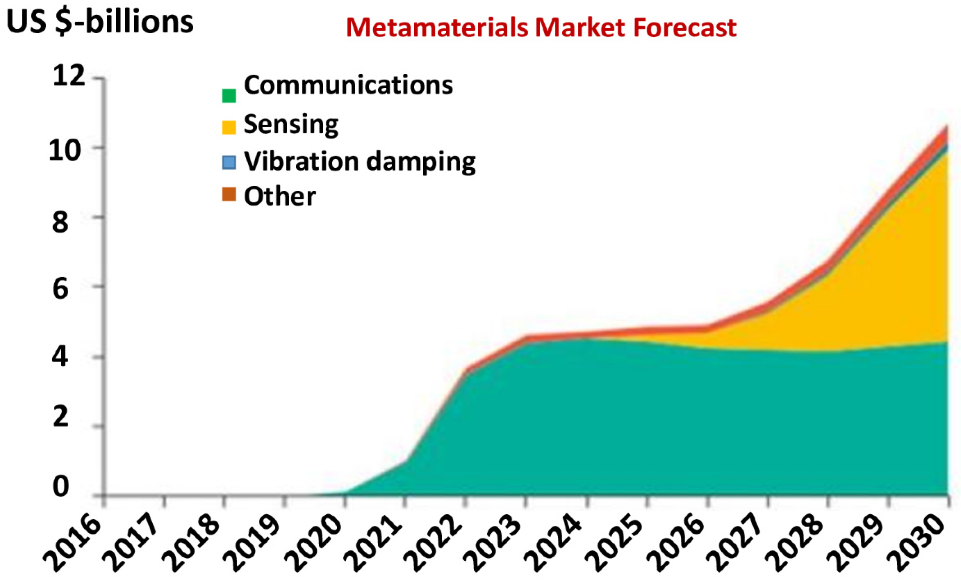
- Vicari, A.; Holman, M.; Schiavo, A. Metamaterials Market Forecast, 2019. Available online: https://web.luxresearchinc.com/hubfs/Press%20Release%20Assets/Lux%20Research%20Metamaterials%20Market%20Forecast%20Executive%20Summary.pdf (accessed on 1 January 2021).
- Pendry, J.B. Negative Refraction Makes a Perfect Lens. Phys. Rev. Lett. 2000, 85, 3966–3969. [Google Scholar] [CrossRef] [PubMed]
- Leonhardt, U. Invisibility cup. Nat. Photonics 2007, 1, 207–208. [Google Scholar] [CrossRef]
- Grebenchukov, A.; Masyukov, M.; Zaitsev, A.; Khodzitsky, M. Asymmetric graphene metamaterial for narrowband terahertz modulation. Opt. Commun. 2020, 476, 126299. [Google Scholar] [CrossRef]
- Modi, A.Y.; Balanis, C.A.; Birtcher, C.R.; Shaman, H.N. Novel Design of Ultrabroadband Radar Cross Section Reduction Surfaces Using Artificial Magnetic Conductors. IEEE Trans. Antennas Propag. 2017, 65, 5406–5417. [Google Scholar] [CrossRef]
- Morawiec, S.; Crupi, I. Light trapping by plasmonic nanoparticles. In Solar Cells and Light Management: Materials, Strategies and Sustainability; Enrichi, F., Righini, G., Eds.; Elsevier: Amsterdam, The Netherlands, 2020; Chapter 8; pp. 277–313. ISBN 978-0-08-102762-2. [Google Scholar]
- Uhrenfeldt, C.; Villesen, T.F.; Têtu, A.; Johansen, B.; Larsen, A.N. Broadband photocurrent enhancement and light-trapping in thin film Si solar cells with periodic Al nanoparticle arrays on the front. Opt. Express 2015, 23, A525–A538. [Google Scholar] [CrossRef] [PubMed]
- Li, Y.; Zhang, J.; Zhang, Y.; Hongya, C.; Fan, Y. Wideband, co-polarization anomalous reflection metasurface based on low-Q resonators. Appl. Phys. A 2016, 122, 851. [Google Scholar] [CrossRef]
- Muhammad, N.; Khan, A.D. Tunable Fano Resonances and Electromagnetically Induced Transparency in All-Dielectric Holey Block. Plasmonics 2015, 10, 1687–1693. [Google Scholar] [CrossRef]
- Khan, A.D.; Amin, M.; Ali, A.; Khan, S.D.; Khan, R. Multiple higher-order Fano resonances in plasmonic hollow cylindrical nanodimer. Appl. Phys. A 2015, 120, 641–649. [Google Scholar] [CrossRef]
- Feng, M.; Li, Y.; Zheng, Q.; Zhang, J.; Han, Y.; Wang, J.; Hongya, C.; Sui, S.; Ma, H.; Qu, S. Two-dimensional Coding phase gradient metasurface for RCS reduction. J. Phys. D Appl. Phys. 2018, 51, 375103. [Google Scholar] [CrossRef]
- Kang, E.; Chaharsoughi, M.; Rossi, S.; Jonsson, M. Hybrid plasmonic metasurfaces. J. Appl. Phys. 2019, 126, 140901. [Google Scholar] [CrossRef]
- Luo, X.; Pu, M.; Ma, X.; Li, X. Taming the Electromagnetic Boundaries via Metasurfaces: From Theory and Fabrication to Functional Devices. Int. J. Antennas Propag. 2015, 2015, 204127. [Google Scholar] [CrossRef]
- Holloway, C.; Kuester, E.; Gordon, J.; O’Hara, J.; Booth, J.; Smith, D. An Overview of the Theory and Applications of Metasurfaces: The Two-Dimensional Equivalents of Metamaterials. Antennas Propag. Mag. IEEE 2012, 54, 10–35. [Google Scholar] [CrossRef]
- Bukhari, S.; Vardaxoglou, J.; Whittow, W. A Metasurfaces Review: Definitions and Applications. Appl. Sci. 2019, 9, 2727. [Google Scholar] [CrossRef] [Green Version]
- Ladumor, M.; Charola, S.; Patel, S.; Dhasarathan, V. Graphene-based c-shaped metasurface broadband solar absorber. Proc. SPIE 2020, 11274. [Google Scholar] [CrossRef]
- Quarfoth, R.; Sievenpiper, D. Artificial Tensor Impedance Surface Waveguides. IEEE Trans. Antennas Propag. 2013, 61, 3597–3606. [Google Scholar] [CrossRef]
- Maksimenko, O.; Shcherbinin, V.; Tkachenko, V. Coupled-Mode Theory of an Irregular Waveguide with Impedance Walls. J. Infrared Millim. Terahertz Waves 2019, 40, 620–636. [Google Scholar] [CrossRef]
- Chen, J.; Zhao, Y.; Xing, L.; He, Z.; Sun, L. Broadband bifunctional Luneburg–Fisheye lens based on anisotropic metasurface. Sci. Rep. 2020, 10, 20381. [Google Scholar] [CrossRef]
- Taheri, M.L.; McGowan, S.; Nikolova, L.; Evans, J.E.; Teslich, N.; Lu, J.P.; LaGrange, T.; Rosei, F.; Siwick, B.J.; Browning, N.D. In situ laser crystallization of amorphous silicon: Controlled nanosecond studies in the dynamic transmission electron microscope. Appl. Phys. Lett. 2010, 97, 032102. [Google Scholar] [CrossRef] [Green Version]
- Chen, H.-T.; Taylor, A.J.; Yu, N. A review of metasurfaces: Physics and applications. Rep. Prog. Phys. 2016, 79, 76401. [Google Scholar] [CrossRef] [Green Version]
- Alici, K.B.; Özbay, E. Radiation properties of a split ring resonator and monopole composite. Phys. Status Solidi 2007, 244, 1192–1196. [Google Scholar] [CrossRef]
- Alici, K.B.; Serebryannikov, A.E.; Ozbay, E. Radiation Properties and Coupling Analysis of a Metamaterial Based, Dual Polarization, Dual Band, Multiple Split Ring Resonator Antenna. J. Electromagn. Waves Appl. 2010, 24, 1183–1193. [Google Scholar] [CrossRef]
- Xiao, S.; Wang, T.; Liu, T.; Chaobiao, Z.; Jiang, X.; Zhang, J. Active metamaterials and metadevices: A review. J. Phys. D Appl. Phys. 2020, 53, 503002. [Google Scholar] [CrossRef]
- Li, Y.; Liu, Z.; Pan, P.; Liu, X.; Fu, G.; Liu, Z.; Luo, H.; Liu, G. Semiconductor-nanoantenna-assisted solar absorber for ultra-broadband light trapping. Nanoscale Res. Lett. 2020, 15, 76. [Google Scholar] [CrossRef] [PubMed] [Green Version]
- Landy, N.I.; Sajuyigbe, S.; Mock, J.J.; Smith, D.R.; Padilla, W.J. Perfect Metamaterial Absorber. Phys. Rev. Lett. 2008, 100, 207402. [Google Scholar] [CrossRef] [PubMed]
- Liu, Z.; Lee, H.; Xiong, Y.; Sun, C.; Zhang, X. Far-Field Optical Hyperlens Magnifying Sub-Diffraction-Limited Objects. Science 2007, 315, 1686. [Google Scholar] [CrossRef] [Green Version]
- Nassar, H.; Chen, Y.Y.; Huang, G.L. Polar Metamaterials: A New Outlook on Resonance for Cloaking Applications. Phys. Rev. Lett. 2020, 124, 84301. [Google Scholar] [CrossRef] [Green Version]
- Cai, W.; Chettiar, U.K.; Kildishev, A.V.; Shalaev, V.M. Optical cloaking with metamaterials. Nat. Photonics 2007, 1, 224–227. [Google Scholar] [CrossRef] [Green Version]
- Jiang, L.; Chu, C.; Fang, B.; Zhang, M.; Gan, H.; Li, C.; Jing, X.; Hong, Z. Multi-wavelength carpet cloaking based on an ultrathin single layer metamaterial microstructure. Laser Phys. Lett. 2020, 17, 66202. [Google Scholar] [CrossRef]
- Karamanos, T.; Amanatiadis, S.; Zygiridis, T.; Kantartzis, N. Quadrupolarisability extraction for planar metamaterial scatterers via far-field response. COMPEL-Int. J. Comput. Math. Electr. Electron. Eng. 2020, 39, 647–657. [Google Scholar] [CrossRef]
- Aïssa, B.; El Khakani, M.A. The channel length effect on the electrical performance of suspended-single-wall-carbon-nanotube-based field effect transistors. Nanotechnology 2009, 20, 175203. [Google Scholar] [CrossRef] [PubMed]
- Lee, T.G.; Jo, S.-H.; Seung, H.; Kim, S.-W.; Kim, E.; Youn, B.D.; Nahm, S.; Kim, M. Enhanced energy transfer and conversion for high performance phononic crystal-assisted elastic wave energy harvesting. Nano Energy 2020, 105226. [Google Scholar] [CrossRef]
- He, Q.; Sun, S.; Zhou, L. Tunable/Reconfigurable Metasurfaces: Physics and Applications. Research 2019, 2019, 1–16. [Google Scholar] [CrossRef] [PubMed] [Green Version]
- Li, A.; Kim, S.; Luo, Y.; Li, Y.; Long, J.; Sievenpiper, D. High-Power Transistor-Based Tunable and Switchable Metasurface Absorber. IEEE Trans. Microw. Theory Tech. 2017, 65, 2810–2818. [Google Scholar] [CrossRef] [Green Version]
- Zhang, D.; Wang, X. Generation of Tilted High-Order Bessel Beam in Millimeter Range Using Metasurface. In Proceedings of the 2019 IEEE International Symposium on Antennas and Propagation and USNC-URSI Radio Science Meeting, Atlanta, GA, USA, 7–12 July 2019. [Google Scholar]
- Zhao, J.; Cheng, Q.; Chen, J.; Qi, M.Q.; Jiang, W.X.; Cui, T. A Tunable Metamaterial Absorber using Varactor Diodes. New J. Phys. 2013, 15, 43049. [Google Scholar] [CrossRef]
- Habib, M.A.; Barkat, M.; Aissa, B.; Denidni, T. Ca-cfar detection performance of radar targets embedded in “non centered chi-2 gamma” clutter. Prog. Electromagn. Res. 2008, 88, 135–148. [Google Scholar] [CrossRef] [Green Version]
- Pande, S.; Kawitkar, R. A Review of Techniques to Design Tunable Antenna Covered with Metamaterial; Springer: Berlin/Heidelberg, Germany, 2020; pp. 9–20. ISBN 978-981-15-2925-2. [Google Scholar]
- Fan, K.; Strikwerda, A.C.; Zhang, X.; Averitt, R.D. Three-dimensional broadband tunable terahertz metamaterials. Phys. Rev. B 2013, 87, 161104. [Google Scholar] [CrossRef] [Green Version]
- Yang, D.; Xia, Y. Experimental verification of multi-band metamaterial absorber with double structured layers. Mater. Res. Express 2020, 7, 35801. [Google Scholar] [CrossRef]
- Haschke, J.; Lemerle, R.; Aïssa, B.; Abdallah, A.A.; Kivambe, M.M.; Boccard, M.; Ballif, C. Annealing of silicon heterojunction solar cells: Interplay of solar cell and indium tin oxide properties. IEEE J. Photovolt. 2019, 9, 1202–1207. [Google Scholar] [CrossRef]
- Kim, G.M.; van den Boogaart, M.A.F.; Brugger, J. Fabrication and application of a full wafer size micro/nanostencil for multiple length-scale surface patterning. Microelectron. Eng. 2003, 67–68, 609–614. [Google Scholar] [CrossRef] [Green Version]
- Tao, H.; Amsden, J.J.; Strikwerda, A.C.; Fan, K.; Kaplan, D.L.; Zhang, X.; Averitt, R.D.; Omenetto, F.G. Metamaterial Silk Composites at Terahertz Frequencies. Adv. Mater. 2010, 22, 3527–3531. [Google Scholar] [CrossRef] [PubMed]
- Qin, Y.; Pan, A.; Liu, L.; Moutanabbir, O.; Yang, R.B.; Knez, M. Atomic Layer Deposition Assisted Template Approach for Electrochemical Synthesis of Au Crescent-Shaped Half-Nanotubes. ACS Nano 2011, 5, 788–794. [Google Scholar] [CrossRef] [PubMed]
- Won, S.; Jung, H.-J.; Kim, D.; Lee, S.-H.; Van Lam, D.; Kim, H.-D.; Kim, K.-S.; Lee, S.-M.; Seo, M.; Kim, D.-S.; et al. Graphene-based crack lithography for high-throughput fabrication of terahertz metamaterials. Carbon 2020, 158, 505–512. [Google Scholar] [CrossRef]
- Gutruf, P.; Shah, C.M.; Walia, S.; Nili, H.; Zoolfakar, A.S.; Karnutsch, C.; Kalantar-Zadeh, K.; Sriram, S.; Bhaskaran, M. Transparent functional oxide stretchable electronics: Micro-tectonics enabled high strain electrodes. NPG Asia Mater. 2013, 5, e62. [Google Scholar] [CrossRef]
- Aksu, S.; Huang, M.; Artar, A.; Yanik, A.A.; Selvarasah, S.; Dokmeci, M.R.; Altug, H. Flexible Plasmonics on Unconventional and Nonplanar Substrates. Adv. Mater. 2011, 23, 4422–4430. [Google Scholar] [CrossRef] [PubMed]
- Chen, Y.; Ai, B.; Wong, Z.J. Soft optical metamaterials. Nano Converg. 2020, 7, 18. [Google Scholar] [CrossRef]
- Lee, M.H.; Huntington, M.D.; Zhou, W.; Yang, J.-C.; Odom, T.W. Programmable Soft Lithography: Solvent-Assisted Nanoscale Embossing. Nano Lett. 2011, 11, 311–315. [Google Scholar] [CrossRef]
- Chanda, D.; Shigeta, K.; Gupta, S.; Cain, T.; Carlson, A.; Mihi, A.; Baca, A.J.; Bogart, G.R.; Braun, P.; Rogers, J.A. Large-area flexible 3D optical negative index metamaterial formed by nanotransfer printing. Nat. Nanotechnol. 2011, 6, 402–407. [Google Scholar] [CrossRef]
- Scheuer, J. Optical Metasurfaces Are Coming of Age: Short- and Long-Term Opportunities for Commercial Applications. ACS Photonics 2020, 7, 1323–1354. [Google Scholar] [CrossRef]
- Liu, N.; Guo, H.; Fu, L.; Kaiser, S.; Schweizer, H.; Giessen, H. Three-dimensional photonic metamaterials at optical frequencies. Nat. Mater. 2008, 7, 31–37. [Google Scholar] [CrossRef]
- Bordjiba, T.; Mohamedi, M.; Dao, L.H.; Aissa, B.; El Khakani, M.A. Enhanced physical and electrochemical properties of nanostructured carbon nanotubes coated microfibrous carbon paper. Chem. Phys. Lett. 2007, 441, 88–93. [Google Scholar] [CrossRef]
- Kim, M.; Rho, J. Metamaterials and imaging. Nano Converg. 2015, 2, 22. [Google Scholar] [CrossRef] [PubMed] [Green Version]
- Zhang, X.; Liu, Z. Superlenses to overcome the diffraction limit. Nat. Mater. 2008, 7, 435–441. [Google Scholar] [CrossRef]
- Leonhardt, U.; Philbin, T. Quantum Levitation by Left-handed Metamaterials. New J. Phys. 2006, 9, 254. [Google Scholar] [CrossRef]
- Peralta, X.G.; Wanke, M.C.; Arrington, C.L.; Williams, J.D.; Brener, I.; Strikwerda, A.; Averitt, R.D.; Padilla, W.J.; Smirnova, E.; Taylor, A.J.; et al. Large-area metamaterials on thin membranes for multilayer and curved applications at terahertz and higher frequencies. Appl. Phys. Lett. 2009, 94, 161113. [Google Scholar] [CrossRef] [Green Version]
- Ali, A.; Hantanasirisakul, K.; Abdala, A.; Urbankowski, P.; Zhao, M.Q.; Anasori, B.; Gogotsi, Y.; Aïssa, B.; Mahmoud, K.A. Effect of synthesis on performance of MXene/iron oxide anode material for lithium-ion batteries. Langmuir 2018, 34, 11325–11334. [Google Scholar] [CrossRef]
- Shao, D.B.; Chen, S.C. Direct Patterning of Three-Dimensional Periodic Nanostructures by Surface-Plasmon-Assisted Nanolithography. Nano Lett. 2006, 6, 2279–2283. [Google Scholar] [CrossRef]
- Wei, F.; Lu, D.; Shen, H.; Wan, W.; Ponsetto, J.L.; Huang, E.; Liu, Z. Wide Field Super-Resolution Surface Imaging through Plasmonic Structured Illumination Microscopy. Nano Lett. 2014, 14, 4634–4639. [Google Scholar] [CrossRef]
- Pryce, I.M.; Aydin, K.; Kelaita, Y.A.; Briggs, R.M.; Atwater, H.A. Highly Strained Compliant Optical Metamaterials with Large Frequency Tunability. Nano Lett. 2010, 10, 4222–4227. [Google Scholar] [CrossRef] [Green Version]
- Xu, X.; Yang, Q.; Wattanatorn, N.; Zhao, C.; Stewart, L.A.; Jonas, S.J.; Weiss, P.S. Methods for Multiple-Patterning Nanosphere Lithography for Fabrication of Periodic Three-Dimensional Hierarchical Nanostructures. U.S. Patent 20,200,098,577A1, 1 April 2020. [Google Scholar]
- Aïssa, B.; Therriault, D.; Farahani, R.D.; Lebel, L.L.; El Khakani, M.A. Electrical transport properties of single wall carbon nanotube/polyurethane composite based field effect transistors fabricated by UV-assisted direct-writing technology. Nanotechnology 2012, 23, 115705. [Google Scholar] [CrossRef]
- Lebel, L.L.; Aïssa, B.; El Khakani, M.A.; Therriault, D. Ultraviolet-assisted direct-write fabrication of carbon nanotube/polymer nanocomposite micro-coils. Adv. Mater. 2010, 22, 592. [Google Scholar] [CrossRef]
- Burckel, D.B.; Sinclair, M.B. Modeling study of multi-layer 3D metamaterials. Proc. SPIE 2011, 8093, 809317. [Google Scholar] [CrossRef]
- Lio, G.E.; Ferraro, A.; Ritacco, T.; Aceti, D.; De Luca, A.; Giocondo, M.; Caputo, R. Leveraging on ENZ Metamaterials to Achieve 2D and 3D Hyper-Resolution in Two-Photon Direct Laser Writing. Adv. Mater. 2021, 33, 2008644. [Google Scholar] [CrossRef]
- Chu, C.H.; Tseng, M.L.; Chen, J.; Wu, P.C.; Chen, Y.-H.; Wang, H.-C.; Chen, T.-Y.; Hsieh, W.T.; Wu, H.J.; Sun, G.; et al. Active dielectric metasurface based on phase-change medium. Laser Photonics Rev. 2016, 10, 986–994. [Google Scholar] [CrossRef]
- Zhou, Z.; Wang, S.; Yu, Y.; Chen, Y.; Feng, L. High performance metamaterials-high electron mobility transistors integrated terahertz modulator. Opt. Express 2017, 25, 17832–17840. [Google Scholar] [CrossRef] [PubMed]
- de Galarreta, C.R.; Alexeev, A.M.; Au, Y.-Y.; Lopez-Garcia, M.; Klemm, M.; Cryan, M.; Bertolotti, J.; Wright, C.V. Nonvolatile Reconfigurable Phase-Change Metadevices for Beam Steering in the Near Infrared. Adv. Funct. Mater. 2018, 28, 1704993. [Google Scholar] [CrossRef] [Green Version]
- Ali, A.; Jo, J.; Yang, Y.J.; Choi, K.H. Direct fabrication of graphene/zinc oxide composite film and its characterizations. Appl. Phys. A 2014, 114, 323–330. [Google Scholar] [CrossRef]
- Lee, K.-T.; Park, D.H.; Baac, H.W.; Han, S. Graphene- and Carbon-Nanotube-Based Transparent Electrodes for Semitransparent Solar Cells. Materials 2018, 11, 1503. [Google Scholar] [CrossRef] [Green Version]
- Minovich, A.; Farnell, J.; Neshev, D.N.; McKerracher, I.; Karouta, F.; Tian, J.; Powell, D.A.; Shadrivov, I.V.; Tan, H.H.; Jagadish, C. Liquid crystal based nonlinear fishnet metamaterials. Appl. Phys. Lett. 2012, 100, 121113. [Google Scholar] [CrossRef] [Green Version]
- Lee, C.-W.; Choi, H.J.; Jeong, H. Tunable metasurfaces for visible and SWIR applications. Nano Converg. 2020, 7, 3. [Google Scholar] [CrossRef] [Green Version]
- Vest, B. Levelized Cost and Levelized Avoided Cost of New Generation Resources in the Annual Energy Outlook 2016. US EIA LCOE 2016, 1–20. [Google Scholar]
- Maeda, H.; Tanaka, Y.; Fukutomi, M.; Asano, T. A New High-TcOxide Superconductor without a Rare Earth Element. Jpn. J. Appl. Phys. 1988, 27, L209–L210. [Google Scholar] [CrossRef] [Green Version]
- Kumar, S.; Lee, H.P. The Present and Future Role of Acoustic Metamaterials for Architectural and Urban Noise Mitigations. Acoustics 2019, 1, 590–607. [Google Scholar] [CrossRef] [Green Version]
- Ou, J.Y.; Plum, E.; Jiang, L.; Zheludev, N.I. Reconfigurable Photonic Metamaterials. Nano Lett. 2011, 11, 2142–2144. [Google Scholar] [CrossRef]
- Rong, J.; Ye, W.; Zhang, S.; Liu, Y. Frequency-Coded Passive Multifunctional Elastic Metasurfaces. Adv. Funct. Mater. 2020, 30, 2005285. [Google Scholar] [CrossRef]
- Shirmanesh, G.K.; Sokhoyan, R.; Wu, P.C.; Atwater, H.A. Electro-optically Tunable Multifunctional Metasurfaces. ACS Nano 2020, 14, 6912–6920. [Google Scholar] [CrossRef]
- Wang, X.; Wang, H.; Jian, J.; Rutherford, B.X.; Gao, X.; Xu, X.; Zhang, X.; Wang, H. Metal-Free Oxide-Nitride Heterostructure as a Tunable Hyperbolic Metamaterial Platform. Nano Lett. 2020, 20, 6614–6622. [Google Scholar] [CrossRef]
- Zahra, S.; Ma, L.; Wang, W.; Li, J.; Chen, D.; Liu, Y.; Zhou, Y.; Li, N.; Huang, Y.; Wen, G. Electromagnetic Metasurfaces and Reconfigurable Metasurfaces: A Review. Front. Phys. 2021, 8. [Google Scholar] [CrossRef]
- Tao, H.; Strikwerda, A.C.; Fan, K.; Padilla, W.J.; Zhang, X.; Averitt, R.D. Reconfigurable Terahertz Metamaterials. Phys. Rev. Lett. 2009, 103, 147401. [Google Scholar] [CrossRef] [Green Version]
- He, X.; Lv, Z.; Liu, B.; Li, Z. Tunable magnetic metamaterial based multi-split-ring resonator (MSRR) using MEMS switch components. Microsyst. Technol. 2011, 17, 1263–1269. [Google Scholar] [CrossRef]
- Zhu, W.M.; Liu, A.Q.; Zhang, X.M.; Tsai, D.P.; Bourouina, T.; Teng, J.H.; Zhang, X.H.; Guo, H.C.; Tanoto, H.; Mei, T.; et al. Switchable Magnetic Metamaterials Using Micromachining Processes. Adv. Mater. 2011, 23, 1792–1796. [Google Scholar] [CrossRef] [PubMed]
- Yao, D.; Yan, K.; Liu, X.; Liao, S.; Yu, Y.; Lin, Y.-S. Tunable terahertz metamaterial by using asymmetrical double split-ring resonators (ADSRRs). OSA Contin. 2018, 1, 349–357. [Google Scholar] [CrossRef]
- Chen, H.-T.; Padilla, W.J.; Zide, J.M.O.; Gossard, A.C.; Taylor, A.J.; Averitt, R.D. Active terahertz metamaterial devices. Nature 2006, 444, 597–600. [Google Scholar] [CrossRef] [PubMed] [Green Version]
- Wu, J.; Wang, Y. Optical Absorption and Thermal Effects of Plasmonic Nanostructures. In Nanoplasmonics: Fundamentals and Applications; Intech Open: London, UK, 2017; Chapter 7; pp. 157–171. [Google Scholar] [CrossRef] [Green Version]
- Sámson, Z.L.; MacDonald, K.F.; De Angelis, F.; Gholipour, B.; Knight, K.; Huang, K.C.-C.; Di Fabrizio, E.; Hewak, D.W.; Zheludev, N.I. Metamaterial electro-optic switch of nanoscale thickness. Appl. Phys. Lett. 2010, 96, 143105. [Google Scholar] [CrossRef] [Green Version]
- Tie, W.; Bhattacharyya, S.; Lim, Y.; Sang Won, L.; Lee, T.H.; Lee, Y.; Lee, S. Dynamic electro-optic response of graphene/graphitic flakes in nematic liquid crystals. Opt. Express 2013, 21, 19867–19879. [Google Scholar] [CrossRef] [Green Version]
- Shrekenhamer, D.; Rout, S.; Strikwerda, A.C.; Bingham, C.; Averitt, R.D.; Sonkusale, S.; Padilla, W.J. High speed terahertz modulation from metamaterials with embedded high electron mobility transistors. Opt. Express 2011, 19, 9968–9975. [Google Scholar] [CrossRef]
- Yan, H.; Li, X.; Chandra, B.; Tulevski, G.; Wu, Y.; Freitag, M.; Zhu, W.; Avouris, P.; Xia, F. Tunable infrared plasmonic devices using graphene/insulator stacks. Nat. Nanotechnol. 2012, 7, 330–334. [Google Scholar] [CrossRef] [Green Version]
- Xiao, B.; Tong, S.; Fyffe, A.; Shi, Z. Tunable electromagnetically induced transparency based on graphene metamaterials. Opt. Express 2020, 28, 4048–4057. [Google Scholar] [CrossRef]
- Ju, L.; Geng, B.; Horng, J.; Girit, C.; Martin, M.; Hao, Z.; Bechtel, H.A.; Liang, X.; Zettl, A.; Shen, Y.R.; et al. Graphene plasmonics for tunable terahertz metamaterials. Nat. Nanotechnol. 2011, 6, 630–634. [Google Scholar] [CrossRef]
- Bennett, P.J.; Dhanjal, S.; Petropoulos, P.; Richardson, D.J.; Zheludev, N.I.; Emelyanov, V.I. A photonic switch based on a gigantic, reversible optical nonlinearity of liquefying gallium. Appl. Phys. Lett. 1998, 73, 1787–1789. [Google Scholar] [CrossRef]
- Krasavin, A.V.; MacDonald, K.F.; Schwanecke, A.S.; Zheludev, N.I. Gallium/aluminum nanocomposite material for nonlinear optics and nonlinear plasmonics. Appl. Phys. Lett. 2006, 89, 31118. [Google Scholar] [CrossRef] [Green Version]
- Boyarsky, M.; Sleasman, T.; Imani, M.; Gollub, J.; Smith, D. Electronically Steered Nyquist Metasurface Antenna. arXiv 2020, arXiv:2007.01911. [Google Scholar]
- Zheludev, N.I.; Kivshar, Y.S. From metamaterials to metadevices. Nat. Mater. 2012, 11, 917–924. [Google Scholar] [CrossRef]
- Zhang, F.; Xie, X.; Pu, M.; Guo, Y.; Ma, X.; Li, X.; Luo, J.; He, Q.; Yu, H.; Luo, X. Multistate Switching of Photonic Angular Momentum Coupling in Phase-Change Metadevices. Adv. Mater. 2020, 32, 1908194. [Google Scholar] [CrossRef]
- Hannonen, A.; Partanen, H.; Leinonen, A.; Heikkinen, J.; Hakala, T.K.; Friberg, A.T.; Setälä, T. Measurement of the Pancharatnam—Berry phase in two-beam interference. Optica 2020, 7, 1435–1439. [Google Scholar] [CrossRef]
- Devlin, R.C.; Ambrosio, A.; Rubin, N.A.; Mueller, J.P.B.; Capasso, F. Arbitrary spin-to-orbital angular momentum conversion of light. Science 2017, 358, 896–901. [Google Scholar] [CrossRef] [PubMed] [Green Version]
- Balthasar Mueller, J.P.; Rubin, N.A.; Devlin, R.C.; Groever, B.; Capasso, F. Metasurface Polarization Optics: Independent Phase Control of Arbitrary Orthogonal States of Polarization. Phys. Rev. Lett. 2017, 118, 113901. [Google Scholar] [CrossRef] [PubMed] [Green Version]
- Zhang, F.; Pu, M.; Luo, J.; Yu, H.; Luo, X. Symmetry breaking of photonic spin-orbit interactions in metasurfaces. Opto-Electron. Eng. 2017, 44, 319–325. [Google Scholar] [CrossRef]
- Choi, C.; Lee, S.-Y.; Mun, S.-E.; Lee, G.-Y.; Sung, J.; Yun, H.; Yang, J.-H.; Kim, H.-O.; Hwang, C.-Y.; Lee, B. Metasurface with nanostructured Ge2Sb2Te5 as a platform for broadband-operating wavefront switch. Adv. Opt. Mater. 2019, 7, 1900171. [Google Scholar] [CrossRef]
- Li, J.; Kamin, S.; Zheng, G.; Neubrech, F.; Zhang, S.; Liu, N. Addressable metasurfaces for dynamic holography and optical information encryption. Sci. Adv. 2018, 4, eaar6768. [Google Scholar] [CrossRef] [Green Version]
- Yin, X.; Steinle, T.; Huang, L.; Taubner, T.; Wuttig, M.; Zentgraf, T.; Giessen, H. Beam switching and bifocal zoom lensing using active plasmonic metasurfaces. Light Sci. Appl. 2017, 6, e17016. [Google Scholar] [CrossRef] [PubMed]
- Chen, Y.; Li, X.; Sonnefraud, Y.; Fernández-Domínguez, A.I.; Luo, X.; Hong, M.; Maier, S.A. Engineering the Phase Front of Light with Phase-Change Material Based Planar lenses. Sci. Rep. 2015, 5, 8660. [Google Scholar] [CrossRef] [PubMed] [Green Version]
- Lin, H.; Sturmberg, B.C.P.; Lin, K.-T.; Yang, Y.; Zheng, X.; Chong, T.K.; de Sterke, C.M.; Jia, B. A 90-nm-thick graphene metamaterial for strong and extremely broadband absorption of unpolarized light. Nat. Photonics 2019, 13, 270–276. [Google Scholar] [CrossRef]
- Li, W.; Wang, P.; Yao, C.; Zhang, Y.; Tang, H. Experimental investigation of 1D, 2D, and 3D metamaterials for efficiency enhancement in a 6.78MHz wireless power transfer system. Appl. Sci. 2020, 10, 8506. [Google Scholar] [CrossRef]
- Chen, H.-T.; Padilla, W.J.; Zide, J.M.O.; Bank, S.R.; Gossard, A.C.; Taylor, A.J.; Averitt, R.D. Ultrafast optical switching of terahertz metamaterials fabricated on ErAs/GaAs nanoisland superlattices. Opt. Lett. 2007, 32, 1620–1622. [Google Scholar] [CrossRef] [PubMed]
- Padilla, W.J.; Taylor, A.J.; Highstrete, C.; Lee, M.; Averitt, R.D. Dynamical Electric and Magnetic Metamaterial Response at Terahertz Frequencies. Phys. Rev. Lett. 2006, 96, 107401. [Google Scholar] [CrossRef]
- Nikolaenko, A.E.; Papasimakis, N.; Atmatzakis, E.; Luo, Z.; Shen, Z.X.; De Angelis, F.; Boden, S.A.; Di Fabrizio, E.; Zheludev, N.I. Nonlinear graphene metamaterial. Appl. Phys. Lett. 2012, 100, 181109. [Google Scholar] [CrossRef] [Green Version]
- Nikolaenko, A.E.; De Angelis, F.; Boden, S.A.; Papasimakis, N.; Ashburn, P.; Di Fabrizio, E.; Zheludev, N.I. Carbon Nanotubes in a Photonic Metamaterial. Phys. Rev. Lett. 2010, 104, 153902. [Google Scholar] [CrossRef] [Green Version]
- Dani, K.M.; Ku, Z.; Upadhya, P.C.; Prasankumar, R.P.; Brueck, S.R.J.; Taylor, A.J. Subpicosecond Optical Switching with a Negative Index Metamaterial. Nano Lett. 2009, 9, 3565–3569. [Google Scholar] [CrossRef] [Green Version]
- Wu, R.Y.; Zhang, L.; Bao, L.; Wu, L.W.; Ma, Q.; Bai, G.D.; Wu, H.T.; Cui, T.J. Digital Metasurface with Phase Code and Reflection—Transmission Amplitude Code for Flexible Full-Space Electromagnetic Manipulations. Adv. Opt. Mater. 2019, 7, 1801429. [Google Scholar] [CrossRef]
- Liu, S.; Xu, H.-X.; Zhang, H.C.; Cui, T.J. Tunable ultrathin mantle cloak via varactor-diode-loaded metasurface. Opt. Express 2014, 22, 13403–13417. [Google Scholar] [CrossRef]
- Luo, Z.; Wang, Q.; Zhang, X.G.; Wu, J.W.; Dai, J.Y.; Zhang LWu, H.T.; Zhang, H.C.; Ma, H.F.; Cheng, Q.; Cui, T.J. Intensity-Dependent Metasurface with Digitally Reconfigurable Distribution of Nonlinearity. Adv. Opt. Mater. 2019, 7, 1900792. [Google Scholar] [CrossRef]
- John, S. Strong localization of photons in certain disordered dielectric superlattices. Phys. Rev. Lett. 1987, 58, 2486–2489. [Google Scholar] [CrossRef] [PubMed] [Green Version]
- Srivastava, R.; Thapa, K.; Pati, S.; Ojha, S. Omni-direction reflection in one dimensional photonic crystal. Prog. Electromagn. Res. B 2008, 7. [Google Scholar] [CrossRef] [Green Version]
- Fink, Y.; Winn, J.N.; Fan, S.; Chen, C.; Michel, J.; Joannopoulos, J.D.; Thomas, E.L. A dielectric omnidirectional reflector. Science 1998, 282, 1679–1682. [Google Scholar] [CrossRef] [PubMed] [Green Version]
- Joannopoulos, J.D.; Meade, R.D.; Winn, J.N. Photonic Crystals: Molding the Flow of Light, 2nd ed.; Princeton University Press: Princeton, NJ, USA, 1995; ISBN 978-0-691-12456-8. [Google Scholar]
- Yablonovitch, E. Inhibited Spontaneous Emission in Solid-State Physics and Electronics. Phys. Rev. Lett. 1987, 58, 2059–2062. [Google Scholar] [CrossRef] [Green Version]
- Winn, J.N.; Fink, Y.; Fan, S.; Joannopoulos, J.D. Omnidirectional reflection from a one-dimensional photonic crystal. Opt. Lett. 1998, 23, 1573–1575. [Google Scholar] [CrossRef]
- Deopura, M.; Ullal, C.K.; Temelkuran, B.; Fink, Y. Dielectric omnidirectional visible reflector. Opt. Lett. 2001, 26, 1197–1199. [Google Scholar] [CrossRef]
- Xiang, Y.; Dai, X.; Wen, S.; Fan, D. Enlargement of zero averaged refractive index gaps in the photonic heterostructures containing negative-index materials. Phys. Rev. E 2007, 76, 56604. [Google Scholar] [CrossRef]
- Li, J.; Zhou, L.; Chan, C.T.; Sheng, P. Photonic Band Gap from a Stack of Positive and Negative Index Materials. Phys. Rev. Lett. 2003, 90, 83901. [Google Scholar] [CrossRef]
- Xiang, Y.; Dai, X.; Wen, S.; Fan, D. Independently tunable omnidirectional multichannel filters based on the fractal multilayers containing negative-index materials. Opt. Lett. 2008, 33, 1255–1257. [Google Scholar] [CrossRef] [PubMed]
- Banerjee, A. Enhanced refractometric optical sensing by using one-dimensional ternary photonic crystals. Prog. Electromagn. Res. 2009, 89, 11–22. [Google Scholar] [CrossRef] [Green Version]
- Xu, K.; Zheng, X.; She, W. Properties of defect modes in one-dimensional photonic crystals containing a defect layer with a negative refractive index. Appl. Phys. Lett. 2004, 85, 6089–6091. [Google Scholar] [CrossRef]
- Wu, C.-J.; Chu, B.-H.; Weng, M.-T. Analysis of Optical Reflection in a Chirped Distributed Bragg Reflector. J. Electromagn. Waves Appl. 2009, 23, 129–138. [Google Scholar] [CrossRef]
- Guida, G.; Priou, A. An Introduction to Photonic Band Gap (PBG)Materials. Prog. Electromagn. Res. 2003, 41, 1–20. [Google Scholar] [CrossRef] [Green Version]
- Ozbay, E.; Temelkuran, B.; Bayindir, M. Microwave Applications of Photonic Crystals. Prog. Electromagn. Res. 2003, 41, 185–209. [Google Scholar] [CrossRef] [Green Version]
- Krumbholz, N.; Gerlach, K.; Rutz, F.; Koch, M.; Piesiewicz, R.; Kürner, T.; Mittleman, D. Omnidirectional terahertz mirrors: A key element for future terahertz communication systems. Appl. Phys. Lett. 2006, 88, 202905. [Google Scholar] [CrossRef]
- Lu, Y.; Huang, M.; Park, S.; Kim, P.; Nahm, T.-U.; Lee, Y.; Rhee, J. Controllable switching behavior of defect modes in one-dimensional heterostructure photonic crystals. J. Appl. Phys. 2007, 101, 36110. [Google Scholar] [CrossRef]
- Awasthi, S.K.; Malaviya, U.; Ojha, S.; Mishra, N.; Singh, B. Design of a tunable polarizer using a one-dimensional nano sized photonic bandgap structure. Prog. Electromagn. Res. B 2008, 5, 133–152. [Google Scholar] [CrossRef] [Green Version]
- Liu, C.-C.; Chang, Y.-H.; Wu, C.-J. Refractometric Optical Sensing by using a Multilayer Reflection and Transmission Narrowband Filter. J. Electromagn. Waves Appl. 2010, 24, 293–305. [Google Scholar] [CrossRef]
- Wu, C.-J.; Chu, B.-H.; Weng, M.-T.; Lee, H.-L. Enhancement of Bandwidth in a Chirped Quarter-Wave Dielectric Mirror. J. Electromagn. Waves Appl. 2009, 23, 437–447. [Google Scholar] [CrossRef]
- Wang, X.; Hu, X.; Li, Y.; Jia, W.; Xu, C.; Liu, X.; Zi, J. Enlargement of omnidirectional total reflection frequency range in one-dimensional photonic crystals by using photonic heterostructures. Appl. Phys. Lett. 2002, 80, 4291–4293. [Google Scholar] [CrossRef]
- Zi, J.; Wan, J.; Zhang, C. Large frequency range of negligible transmission in one-dimensional photonic quantum well structures. Appl. Phys. Lett. 1998, 73, 2084–2086. [Google Scholar] [CrossRef] [Green Version]
- Srivastava, R.; Pratap, U.; Ojha, S. Enhancement of omnidirectional reflection in photonic crystal heterostructures. Prog. Electromagn. Res. B 2008, 1, 197–208. [Google Scholar] [CrossRef] [Green Version]
- Wu, C.-J.; Rau, Y.-N.; Han, W.-H. Enhancement of Photonic Band Gap in a Disordered Quarter-Wave Dielectric Photonic Crystal. Prog. Electromagn. Res. 2010, 100, 27–36. [Google Scholar] [CrossRef] [Green Version]
- Li, H.; Chen, H.; Qiu, X. Band-gap extension of disordered 1D binary photonic crystals. Phys. B Condens. Matter 2000, 279, 164–167. [Google Scholar] [CrossRef]
- Banerjee, A. Enhanced Incidence Angle Based Spectrum Tuning by Using One-Dimensional Ternary Photonic Band Gap Structures. J. Electromagn. Waves Appl. 2010, 24, 1023–1032. [Google Scholar] [CrossRef]
- Xiang, Y.J.; Dai, X.; Wen, S.; Tang, Z.; Fan, D. Extending the zero-effective-phase photonic bandgap by one-dimensional ternary photonic crystals. Appl. Phys. B 2011, 103, 897–906. [Google Scholar] [CrossRef]
- Awasthi, S.K.; Malaviya, U.; Ojha, S.P. Enhancement of omnidirectional total-reflection wavelength range by using one-dimensional ternary photonic bandgap material. J. Opt. Soc. Am. B 2006, 23, 2566–2571. [Google Scholar] [CrossRef]
- Awasthi, S.K.; Ojha, S. Design of a tunable optical filter by using one-dimensional ternary photonic band gap material. Prog. Electromagn. Res. M 2008, 4, 117–132. [Google Scholar] [CrossRef] [Green Version]
- Wu, C.-J.; Chung, Y.-H.; Syu, B.-J.; Yang, T.-J. Band gap extension in a one-dimensional ternary metal-dielectric photonic crystal. Prog. Electromagn. Res. 2010, 102, 81–93. [Google Scholar] [CrossRef] [Green Version]
- Kong, X.-K.; Liu, S.-B.; Feng, Z.; Li, C.; Bian, B. Omnidirectional photonic band gap of one-dimensional ternary plasma photonic crystals. J. Opt. 2011, 13, 35101. [Google Scholar] [CrossRef]
- Bowden, C.; Dowling, J.; Everitt, H. Development and Applications of Materials Exhibiting Photonic Band Gaps Introduction. J. Opt. Soc. Am. B Opt. Phys. 1993, 10, 280–282. [Google Scholar] [CrossRef]
- John, S.; Quang, T. Spontaneous emission near the edge of a photonic band gap. Phys. Rev. A 1994, 50, 1764–1769. [Google Scholar] [CrossRef] [PubMed]
- Zhu, S.-Y.; Chen, H.; Huang, H. Quantum Interference Effects in Spontaneous Emission from an Atom Embedded in a Photonic Band Gap Structure. Phys. Rev. Lett. 1997, 79, 205–208. [Google Scholar] [CrossRef]
- John, S.; Quang, T. Collective Switching and Inversion without Fluctuation of Two-Level Atoms in Confined Photonic Systems. Phys. Rev. Lett. 1997, 78, 1888. [Google Scholar] [CrossRef] [Green Version]
- Feng, D.; Yee, S.K.; Zhang, Z.M. Improved performance of a near-field thermophotovoltaic device by a back gapped reflector. Sol. Energy Mater. Sol. Cells 2022, 237, 111562. [Google Scholar] [CrossRef]
- Bierman, D.M.; Lenert, A.; Chan, W.R.; Bhatia, B.; Celanović, I.; Soljačić, M.; Wang, E.N. Enhanced photovoltaic energy conversion using thermally based spectral shaping. Nat. Energy 2016, 1, 16068. [Google Scholar] [CrossRef]
- Bhatt, R.; Kravchenko, I.; Gupta, M. High-efficiency solar thermophotovoltaic system using a nanostructure-based selective emitter. Sol. Energy 2020, 197, 538–545. [Google Scholar] [CrossRef]
- Cornelius, C.M.; Dowling, J.P. Modification of Planck blackbody radiation by photonic band-gap structures. Phys. Rev. A 1999, 59, 4736–4746. [Google Scholar] [CrossRef]
- Lin, S.-Y.; Fleming, J.G.; Chow, E.; Bur, J.; Choi, K.K.; Goldberg, A. Enhancement and suppression of thermal emission by a three-dimensional photonic crystal. Phys. Rev. B 2000, 62, R2243–R2246. [Google Scholar] [CrossRef]
- Pralle, M.U.; Moelders, N.; McNeal, M.P.; Puscasu, I.; Greenwald, A.C.; Daly, J.T.; Johnson, E.A.; George, T.; Choi, D.S.; El-Kady, I.; et al. Photonic crystal enhanced narrow-band infrared emitters. Appl. Phys. Lett. 2002, 81, 4685–4687. [Google Scholar] [CrossRef]
- Lin, S.Y.; Moreno, J.; Fleming, J.G. Three-dimensional photonic-crystal emitter for thermal photovoltaic power generation. Appl. Phys. Lett. 2003, 83, 380–382. [Google Scholar] [CrossRef] [Green Version]
- Lin, S.-Y.; Fleming, J.G.; El-Kady, I. Three-dimensional photonic-crystal emission through thermal excitation. Opt. Lett. 2003, 28, 1909–1911. [Google Scholar] [CrossRef]
- Imada, M.; Noda, S.; Chutinan, A.; Tokuda, T.; Murata, M.; Sasaki, G. Coherent two-dimensional lasing action in surface-emitting laser with triangular-lattice photonic crystal structure. Appl. Phys. Lett. 1999, 75, 316–318. [Google Scholar] [CrossRef]
- Florescu, M.; John, S. Single-atom switching in photonic crystals. Phys. Rev. A 2001, 64, 33801. [Google Scholar] [CrossRef] [Green Version]
- Florescu, M.; John, S. Resonance fluorescence in photonic band gap waveguide architectures: Engineering the vacuum for all-optical switching. Phys. Rev. A 2004, 69, 53810. [Google Scholar] [CrossRef] [Green Version]
- John, S.; Florescu, M. Photonic bandgap materials: Towards an all-optical micro-transistor. J. Opt. A Pure Appl. Opt. 2001, 3, S103–S120. [Google Scholar] [CrossRef]
- Khan, A.D.; Rehman, Q.; Khan, A.D.; Subhan, F.E.; Noman, M.; Ahmed, S.; Khan, H.A. Broadband Solar Energy Absorption in Plasmonic Thin-Film Amorphous Silicon Solar Cell. Coatings 2019, 9, 638. [Google Scholar] [CrossRef] [Green Version]
- Bentouaf, A.; Mebsout, R.; Rached, H.; Amari, S. Theoretical investigation of the structural, electronic, magnetic and elastic properties of binary cubic C15-Laves phases TbX2 (X = Co and Fe). J. Alloys Compd. 2016, 689, 885–893. [Google Scholar] [CrossRef]
- Behaghel, B.; Tamaki, R.; Vandamme, N.; Watanabe, K.; Dupuis, C.; Bardou, N.; Sodabanlu, H.; Cattoni, A.; Okada, Y.; Sugiyama, M.; et al. Absorption enhancement through Fabry-Pérot resonant modes in a 430 nm thick InGaAs/GaAsP multiple quantum wells solar cell. Appl. Phys. Lett. 2015, 106, 81107. [Google Scholar] [CrossRef]
- Fan, R.; Wang, L.; Chen, Y.; Zheng, G.; Li, L.; Li, Z.; Zhou, H. Tailored Au@TiO2 nanostructures for the plasmonic effect in planar perovskite solar cells. J. Mater. Chem. A 2017, 5, 12034–12042. [Google Scholar] [CrossRef]
- Siavash, M.R.; Gholipour, S.; Masudy-Panah, S.; Seza, A.; Mehdikhani, A.; Riahi-Noori, N.; Tafazoli, S.; Timasi, N.; Lim, Y.-F.; Saliba, M. Recent Advances in Plasmonic Perovskite Solar Cells. Adv. Sci. 2020, 7, 1902448. [Google Scholar] [CrossRef]
- Willeke, G.; Nussbaumer, H.; Bender, H.; Bucher, E. A simple and effective light trapping technique for polycrystalline silicon solar cells. Sol. Energy Mater. Sol. Cells 1992, 26, 345–356. [Google Scholar] [CrossRef]
- Zhao, J.; Wang, A.; Altermatt, P.; Green, M.A. Twenty-four percent efficient silicon solar cells with double layer antireflection coatings and reduced resistance loss. Appl. Phys. Lett. 1995, 66, 3636–3638. [Google Scholar] [CrossRef]
- Chutinan, A.; John, S. Light trapping and absorption optimization in certain thin-film photonic crystal architectures. Phys. Rev. A 2008, 78, 23825. [Google Scholar] [CrossRef] [Green Version]
- Duché, D.; Escoubas, L.; Simon, J.-J.; Torchio, P.; Vervisch, W.; Flory, F. Slow Bloch modes for enhancing the absorption of light in thin films for photovoltaic cells. Appl. Phys. Lett. 2008, 92, 193310. [Google Scholar] [CrossRef]
- Akimov, Y.A.; Koh, W.S.; Ostrikov, K. Enhancement of optical absorption in thin-film solar cells through the excitation of higher-order nanoparticle plasmon modes. Opt. Express 2009, 17, 10195–10205. [Google Scholar] [CrossRef] [Green Version]
- Hallermann, F.; Rockstuhl, C.; Fahr, S.; Seifert, G.; Wackerow, S.; Graener, H.; Plessen, G.V.; Lederer, F. On the use of localized plasmon polaritons in solar cells. Phys. Status Solidi 2008, 205, 2844–2861. [Google Scholar] [CrossRef]
- Rockstuhl, C.; Fahr, S.; Lederer, F. Absorption enhancement in solar cells by localized plasmon polaritons. J. Appl. Phys. 2008, 104, 123102. [Google Scholar] [CrossRef]
- Kroll, M.; Fahr, S.; Helgert, C.; Rockstuhl, C.; Lederer, F.; Pertsch, T. Employing dielectric diffractive structures in solar cells—A numerical study. Phys. Status Solidi 2008, 205, 2777–2795. [Google Scholar] [CrossRef]
- Yu, Z.; Raman, A.; Fan, S. Fundamental limit of nanophotonic light-trapping in solar cells. Proc. Natl. Acad. Sci. USA 2010, 107, 17491–17496. [Google Scholar] [CrossRef] [Green Version]
- Battaglia, C.; Escarré, J.; Söderström, K.; Erni, L.; Ding, L.; Bugnon, G.; Billet, A.; Boccard, M.; Barraud, L.; De Wolf, S.; et al. Nanoimprint Lithography for High-Efficiency Thin-Film Silicon Solar Cells. Nano Lett. 2011, 11, 661–665. [Google Scholar] [CrossRef] [PubMed]
- Nechache, R.; Nicklaus, M.; Diffalah, N.; Ruediger, A.; Rosei, F. Pulsed laser deposition growth of rutile TiO2 nanowires on Silicon substrates. Appl. Surf. Sci. 2014, 313, 48–52. [Google Scholar] [CrossRef]
- Zhu, J.; Yu, Z.; Burkhard, G.F.; Hsu, C.-M.; Connor, S.T.; Xu, Y.; Wang, Q.; McGehee, M.; Fan, S.; Cui, Y. Optical Absorption Enhancement in Amorphous Silicon Nanowire and Nanocone Arrays. Nano Lett. 2009, 9, 279–282. [Google Scholar] [CrossRef] [Green Version]
- Jacob, Z.; Kim, J.-Y.; Naik, G.V.; Boltasseva, A.; Narimanov, E.E.; Shalaev, V.M. Engineering photonic density of states using metamaterials. Appl. Phys. B 2010, 100, 215–218. [Google Scholar] [CrossRef] [Green Version]
- Liu, N.; Mesch, M.; Weiss, T.; Hentschel, M.; Giessen, H. Infrared Perfect Absorber and Its Application as Plasmonic Sensor. Nano Lett. 2010, 10, 2342–2348. [Google Scholar] [CrossRef]
- Silalahi, H.; Chen, Y.-P.; CHEN, Y.-S.; Hong, S.; Lin, X.-Y.; Liu, J.-H.; Huang, C.-Y. Floating terahertz metamaterials with extremely large refractive index sensitivities. Photonics Res. 2021, 9, 1970–1978. [Google Scholar] [CrossRef]
- Li, X.; Ying, J.; Liu, J.; Shu, F.; Lang, T.; Jing, X.; Hong, Z. Resonant transparency of a planar anapole metamaterial at terahertz frequencies. Photonics Res. 2020, 9, 125–130. [Google Scholar] [CrossRef]
- Zhang, S.; Zhou, J.; Park, Y.-S.; Rho, J.; Singh, R.; Nam, S.; Azad, A.K.; Chen, H.-T.; Yin, X.; Taylor, A.J.; et al. Photoinduced handedness switching in terahertz chiral metamolecules. Nat. Commun. 2012, 3, 942. [Google Scholar] [CrossRef] [Green Version]
- Cong, L.; Pitchappa, P.; Wu, Y.; Ke, L.; Lee, C.; Singh, N.; Yang, H.; Singh, R. Active Multifunctional Microelectromechanical System Metadevices: Applications in Polarization Control, Wavefront Deflection, and Holograms. Adv. Opt. Mater. 2017, 5, 1600716. [Google Scholar] [CrossRef]
- Yang, Y.; Kim, Y.; Gwak, J.; So, S.; Mun, J.; Kim, M.; Jeong, H.; Kim, I.; Badloe, T.; Rho, J. Realization of Artificial Chirality in Micro-/Nano-Scale Three-Dimensional Plasmonic Structures BT—Chirality, Magnetism and Magnetoelectricity: Separate Phenomena and Joint Effects in Metamaterial Structures; Kamenetskii, E., Ed.; Springer International Publishing: Cham, Switzerland, 2021; pp. 241–263. ISBN 978-3-030-62844-4. [Google Scholar]
- Mun, J.; Rho, J. Importance of higher-order multipole transitions on chiral nearfield interactions. Nanophotonics 2019, 8, 941–948. [Google Scholar] [CrossRef]
- Barron, L.D. Molecular Light Scattering and Optical Activity, 2nd ed.; Cambridge University Press: Cambridge, UK, 2004; ISBN 9780521121378. [Google Scholar]
- Yoo, S.; Park, Q.-H. Metamaterials and chiral sensing: A review of fundamentals and applications. Nanophotonics 2019, 8, 249–261. [Google Scholar] [CrossRef] [Green Version]
- Tester, R.F.; Karkalas, J. Carbohydrates—Classification and Properties. In The Encyclopedia of Food Sciences and Nutrition, 2nd ed.; Caballero, B., Ed.; Academic Press: Oxford, UK, 2003; pp. 862–875. ISBN 978-0-12-227055-0. [Google Scholar]
- Ashalley, E.; Acheampong, K.; Vazquez Besteiro, L.; Yu, P.; Neogi, A.; Govorov, A.; Wang, Z. Multitask deep-learning-based design of chiral plasmonic metamaterials. Photonics Res. 2020, 8, 1213–1225. [Google Scholar] [CrossRef]
- Assouar, B.; Liang, B.; Wu, Y.; Li, Y.; Cheng, J.-C.; Jing, Y. Acoustic metasurfaces. Nat. Rev. Mater. 2018, 3, 460–472. [Google Scholar] [CrossRef] [Green Version]
- Li, Y.; Jiang, X.; Liang, B.; Cheng, J.; Zhang, L. Metascreen-Based Acoustic Passive Phased Array. Phys. Rev. Appl. 2015, 4, 24003. [Google Scholar] [CrossRef]
- Huang, T.-Y.; Shen, C.; Jing, Y. Membrane- and plate-type acoustic metamaterials. J. Acoust. Soc. Am. 2016, 139, 3240–3250. [Google Scholar] [CrossRef] [Green Version]
- Xie, Y.; Popa, B.-I.; Zigoneanu, L.; Cummer, S.A. Measurement of a Broadband Negative Index with Space-Coiling Acoustic Metamaterials. Phys. Rev. Lett. 2013, 110, 175501. [Google Scholar] [CrossRef]
- Asadchy, V.S.; Díaz-Rubio, A.; Tretyakov, S.A. Bianisotropic metasurfaces: Physics and applications. Nanophotonics 2018, 7, 1069–1094. [Google Scholar] [CrossRef]
- Tretyakov, S.A. Nonreciprocal composite with the material relations of the transparent absorbing boundary. Microw. Opt. Technol. Lett. 1998, 19, 365–368. [Google Scholar] [CrossRef]
- Mahmoud, A.M.; Davoyan, A.R.; Engheta, N. All-passive nonreciprocal metastructure. Nat. Commun. 2015, 6, 8359. [Google Scholar] [CrossRef] [PubMed]
- Kodera, T.; Sounas, D.L.; Caloz, C. Artificial Faraday rotation using a ring metamaterial structure without static magnetic field. Appl. Phys. Lett. 2011, 99, 31114. [Google Scholar] [CrossRef]
- Li, Q.; Bao, W.; Nie, Z.; Xia, Y.; Xue, Y.; Wang, Y.; Yang, S.; Zhang, X. A non-unitary metasurface enables continuous control of quantum photon-photon interactions from bosonic to fermionic. Nat. Photonics 2021, 15, 267–271. [Google Scholar] [CrossRef]
- Gansel, J.K.; Thiel, M.; Rill, M.S.; Decker, M.; Bade, K.; Saile, V.; Freymann, G.v.; Linden, S.; Wegener, M. Gold helix photonic metamateri-al as broadband circular polarizer. Science 2009, 325, 1513–1515. [Google Scholar] [CrossRef]
- Li, C.; Yu, P.; Huang, Y.; Zhou, Q.; Wu, J.; Li, Z.; Tong, X.; Wen, Q.; Kuo, H.-C.; Wang, Z.M. Dielectric metasurfaces: From wavefront shaping to quantum platforms. Prog. Surf. Sci. 2020, 95, 100584. [Google Scholar] [CrossRef]
- Lu, C.; Hu, X.; Shi, K.; Hu, Q.; Zhu, R.; Yang, H.; Gong, Q. An actively ultrafast tunable giant slow-light effect in ultrathin nonlinear metasurfaces. Light Sci. Appl. 2015, 4, e302. [Google Scholar] [CrossRef]
- Meng, X.; Depauw, V.; Gomard, G.; El Daif, O.; Trompoukis, C.; Drouard, E.; Jamois, C.; Fave, A.; Dross, F.; Gordon, I.; et al. Design, fabrication and optical characterization of photonic crystal assisted thin film monocrystalline-silicon solar cells. Opt. Express 2012, 20, A465–A475. [Google Scholar] [CrossRef]
- Aïssa, B.; Ali, A.; El Mellouhi, F. Oxide and Organic-Inorganic Halide Perovskites with Plasmonics for Optoelectronic and Energy Applications: A Contributive Review. Catalysts 2021, 11, 1057. [Google Scholar] [CrossRef]
- Kowerdziej, R.; Wróbel, J.; Kula, P. Ultrafast electrical switching of nanostructured metadevice with dual-frequency liquid crystal. Sci. Rep. 2019, 9, 20367. [Google Scholar] [CrossRef] [Green Version]
- Solntsev, A.S.; Agarwal, G.S.; Kivshar, Y.S. Metasurfaces for quantum photonics. Nat. Photonics 2021, 15, 327–336. [Google Scholar] [CrossRef]
- Shrekenhamer, D.; Chen, W.-C.; Padilla, W.J. Liquid Crystal Tunable Metamaterial Absorber. Phys. Rev. Lett. 2013, 110, 177403. [Google Scholar] [CrossRef] [PubMed]
- Wu, J.; Yao, S.; Zhang, H.; Man, W.; Bai, Z.; Zhang, F.; Wang, X.; Fang, D.; Zhang, Y. Liquid Crystal Elastomer Metamaterials with Giant Biaxial Thermal Shrinkage for Enhancing Skin Regeneration. Adv. Mater. 2021, 33, 2106175. [Google Scholar] [CrossRef] [PubMed]
- Miri, M.-A.; Alù, A. Exceptional points in optics and photonics. Science 2019, 363, eaar7709. [Google Scholar] [CrossRef] [PubMed] [Green Version]
- Feng, L.; El-Ganainy, R.; Ge, L. Non-Hermitian photonics based on parity-time symmetry. Nat. Photonics 2017, 11, 752–762. [Google Scholar] [CrossRef]
- Ozdemir, S.; Rotter, S.; Nori, F.; Yang, L. Parity-time symmetry and exceptional points in photonics. Nat. Mater. 2019, 18, 783–798. [Google Scholar] [CrossRef]
- Park, J.-H.; Ndao, A.; Cai, W.; Hsu, L.; Kodigala, A.; Lepetit, T.; Lo, Y.-H.; Kanté, B. Symmetry-breaking-induced plasmonic exceptional points and nanoscale sensing. Nat. Phys. 2020, 16, 462–468. [Google Scholar] [CrossRef]
- Wang, C.; Sweeney, W.; Stone, A.D.; Yang, L. Coherent perfect absorption at an exceptional point. Science 2021, 373, 1261–1265. [Google Scholar] [CrossRef]
- El-Ganainy, R.; Khajavikhan, M.; Christodoulides, D.; Ozdemir, S. The dawn of non-Hermitian optics. Commun. Phys. 2019, 2, 37. [Google Scholar] [CrossRef] [Green Version]
- Lazarides, N.; Tsironis, G.P. Gain-Driven Discrete Breathers in PT-Symmetric Nonlinear Metamaterials. Phys. Rev. Lett. 2013, 110, 53901. [Google Scholar] [CrossRef] [Green Version]
- Yang, F.; Hwang, A.; Doiron, C.; Naik, G.V. Non-Hermitian metasurfaces for the best of plasmonics and dielectrics. Opt. Mater. Express 2021, 11, 2326–2334. [Google Scholar] [CrossRef]
- Baranov, D.; Krasnok, A.; Shegai, T.; Alu, A.; Chong, Y. Coherent perfect absorbers: Linear control of light with light. Nat. Rev. Mater. 2017, 2, 17064. [Google Scholar] [CrossRef] [Green Version]
- Chong, Y.; Ge, L.; Cao, H.; Stone, A.D. Coherent Perfect Absorbers: Time-Reversed Lasers. Phys. Rev. Lett. 2010, 105, 53901. [Google Scholar] [CrossRef] [Green Version]
- Li, C.; Qiu, J.; Ou, J.-Y.; Liu, Q.H.; Zhu, J. High-Sensitivity Refractive Index Sensors Using Coherent Perfect Absorption on Graphene in the Vis-NIR Region. ACS Appl. Nano Mater. 2019, 2, 3231–3237. [Google Scholar] [CrossRef]
- Ioannou, K.; Koukos, I. Metamaterials and Stealth Technology. In Proceedings of the 7th International Conference on “Experiments/Process/System Modeling/Simulation/Optimization” (7th IC-EPSMSO), Athens, Greece, 5–8 July 2017. [Google Scholar]
- Pu, M.; Ma, X.; Li, X.; Guo, Y.; Luo, X. Merging plasmonics and metamaterials by two-dimensional subwavelength structures. J. Mater. Chem. C 2017, 5, 4361–4378. [Google Scholar] [CrossRef]
- Wenjie, W.; Yidong, C.; Li, G.; Heeso, N.; Douglas, S.A.; Hui, C. Time-Reversed Lasing and Interferometric Control of Absorption. Science 2011, 331, 889–892. [Google Scholar] [CrossRef] [Green Version]


Publisher’s Note: MDPI stays neutral with regard to jurisdictional claims in published maps and institutional affiliations. |
© 2022 by the authors. Licensee MDPI, Basel, Switzerland. This article is an open access article distributed under the terms and conditions of the Creative Commons Attribution (CC BY) license (https://creativecommons.org/licenses/by/4.0/).
Share and Cite
Ali, A.; Mitra, A.; Aïssa, B. Metamaterials and Metasurfaces: A Review from the Perspectives of Materials, Mechanisms and Advanced Metadevices. Nanomaterials 2022, 12, 1027. https://doi.org/10.3390/nano12061027
Ali A, Mitra A, Aïssa B. Metamaterials and Metasurfaces: A Review from the Perspectives of Materials, Mechanisms and Advanced Metadevices. Nanomaterials. 2022; 12(6):1027. https://doi.org/10.3390/nano12061027
Chicago/Turabian StyleAli, Adnan, Anirban Mitra, and Brahim Aïssa. 2022. "Metamaterials and Metasurfaces: A Review from the Perspectives of Materials, Mechanisms and Advanced Metadevices" Nanomaterials 12, no. 6: 1027. https://doi.org/10.3390/nano12061027