
Growth Behaviors of GaN on Stripes of Patterned c-Plane GaN Substrate

 ,
, 
Abstract
:1. Introduction
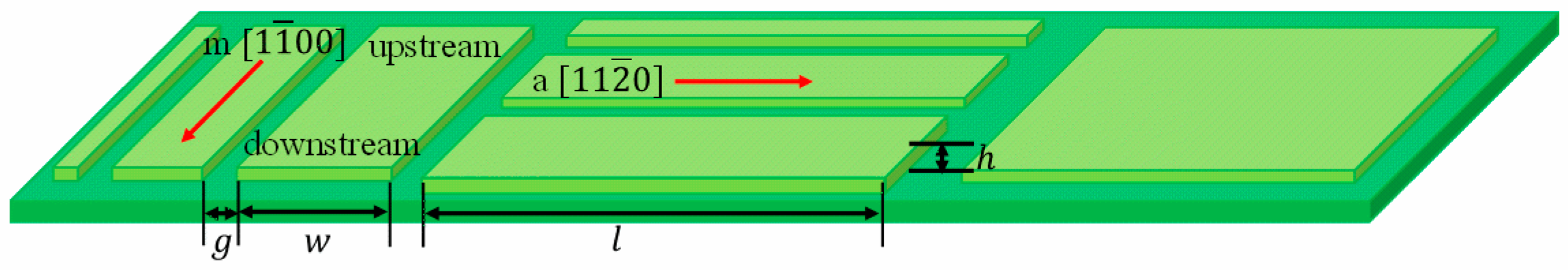
2. Materials and Methods
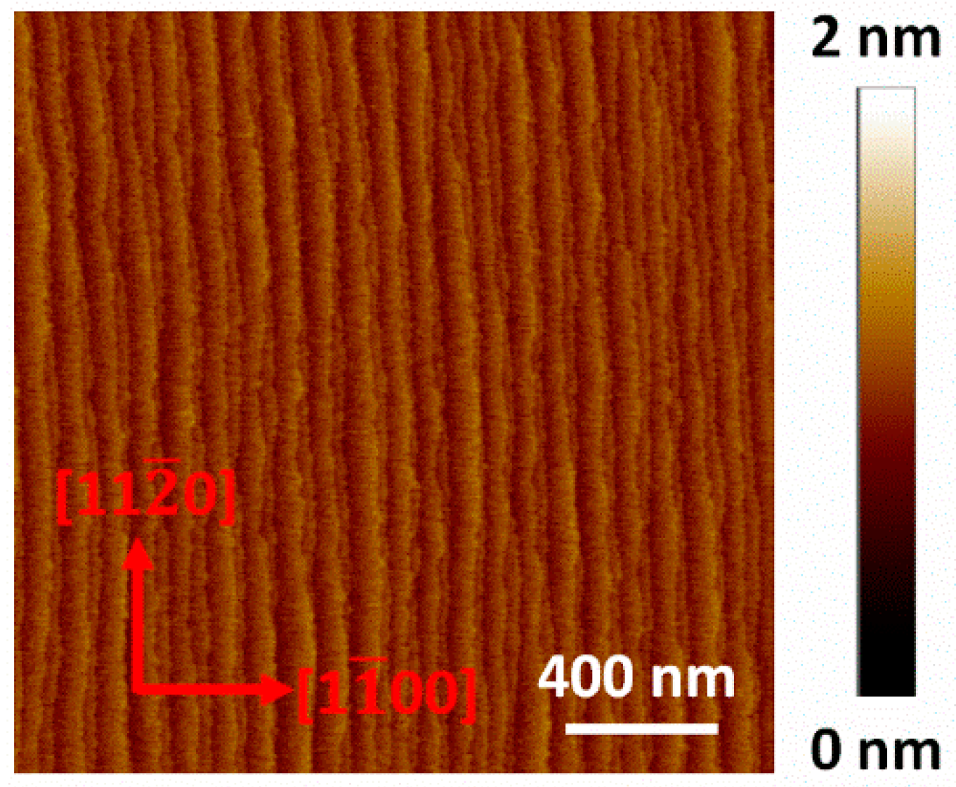
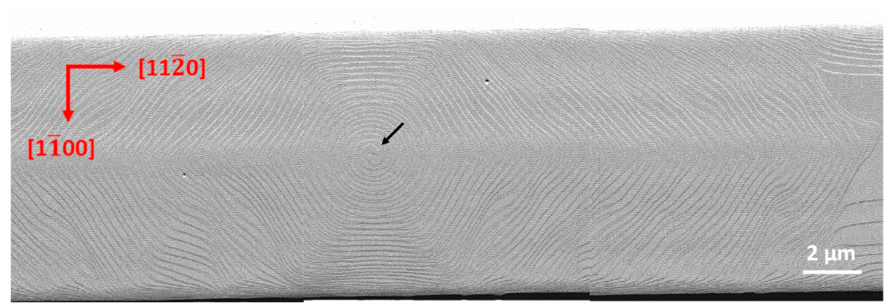
3. Results
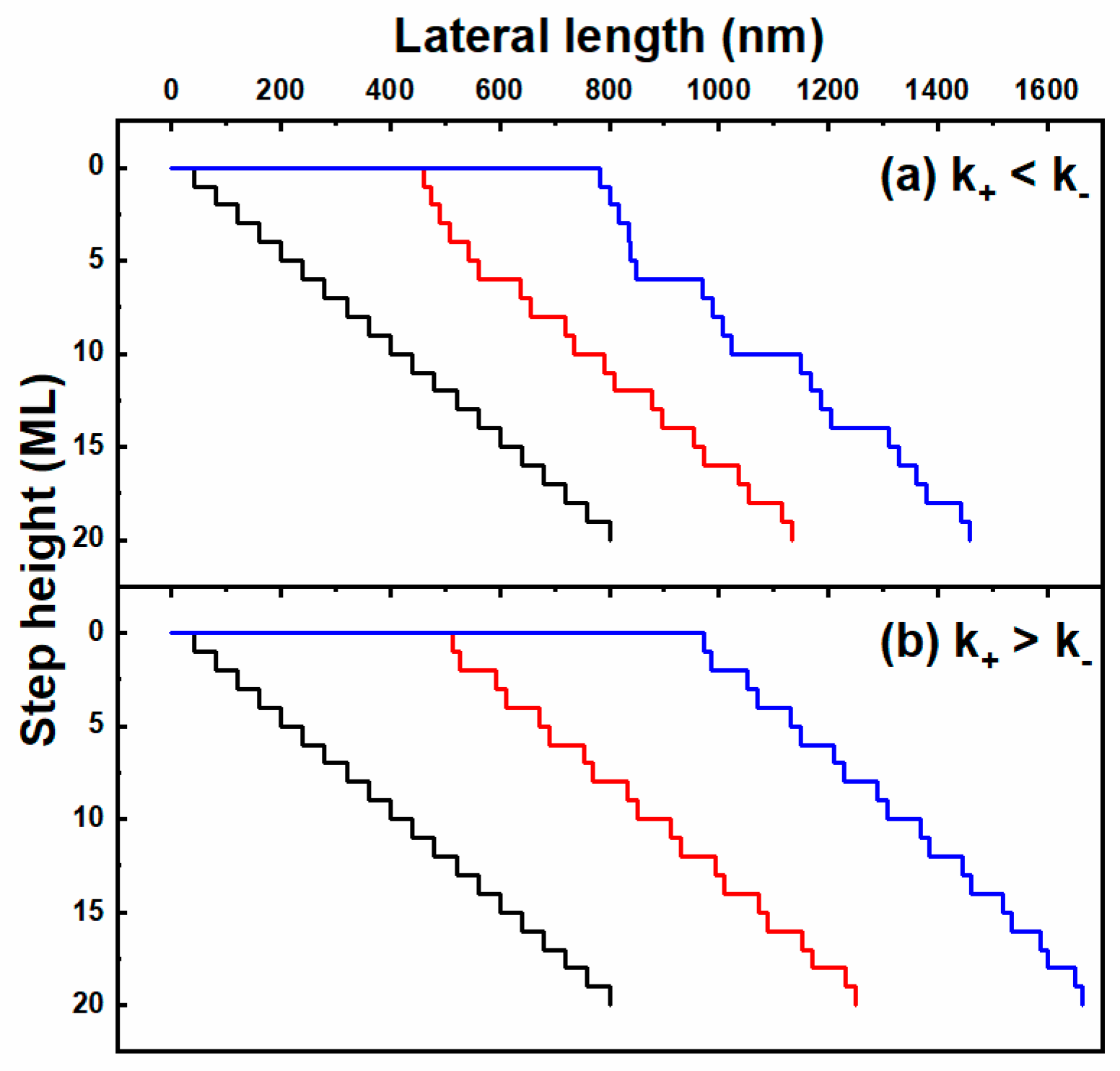
4. Discussion
- (a)
- The probability of adatom incorporation for steps with type A and B edges is different;
- (b)
- When the distance of adjacent steps is shorter than a critical value, step bunching occurs and bunched steps will move with the same speed;
- (c)
- If the terrace width is larger than the atomic diffusion length, only adatoms near steps (the distance from the step being shorter than the diffusion length) can feed the steps.
5. Conclusions
Author Contributions
Funding
Data Availability Statement
Acknowledgments
Conflicts of Interest
References
- Akasaka, T.; Gotoh, H.; Kobayashi, Y.; Yamamoto, H. Extremely narrow violet photoluminescence line from ultrathin InN single quantum well on step-free GaN surface. Adv. Mater. 2012, 24, 4296–4300. [Google Scholar] [CrossRef] [PubMed]
- Saku, T.; Horikoshi, Y.; Tokura, Y. Limit of electron mobility in AlGaAs/GaAs modulation-doped heterostructures. Jpn. J. Appl. Phys. 1996, 35, 34–38. [Google Scholar] [CrossRef]
- Zhou, K.; Liu, J.; Zhang, S.; Li, Z.; Feng, M.; Li, D.; Zhang, L.; Wang, F.; Zhu, J.; Yang, H. Hillock formation and suppression on c-plane homoepitaxial GaN Layers grown by metalorganic vapor phase epitaxy. J. Cryst. Growth 2013, 371, 7–10. [Google Scholar] [CrossRef]
- Jiang, L.; Liu, J.; Tian, A.; Ren, X.; Huang, S.; Zhou, W.; Zhang, L.; Li, D.; Zhang, S.; Ikeda, M.; et al. Influence of substrate misorientation on carbon impurity incorporation and electrical properties of p-GaN grown by metalorganic chemical vapor deposition. Appl. Phys. Express 2019, 12, 55503. [Google Scholar] [CrossRef]
- Hirai, A.; Jia, Z.; Schmidt, M.C.; Farrell, R.M.; DenBaars, S.P.; Nakamura, S.; Speck, J.S.; Fujito, K. Formation and reduction of pyramidal hillocks on m-plane {11¯00} GaN. Appl. Phys. Lett. 2007, 91, 191906. [Google Scholar] [CrossRef]
- Zhou, K.; Liu, J.; Ikeda, M.; Zhang, S.; Li, D.; Zhang, L.; Zeng, C.; Yang, H. Influence of substrate surface defects on the homoepitaxial growth of GaN (0001) by metalorganic vapor phase epitaxy. J. Cryst. Growth 2015, 416, 175–181. [Google Scholar] [CrossRef]
- Turski, H.; Krzyżewski, F.; Feduniewicz-Żmuda, A.; Wolny, P.; Siekacz, M.; Muziol, G.; Cheze, C.; Nowakowski-Szukudlarek, K.; Xing, H.; Jena, D.; et al. Unusual step meandering due to Ehrlich-Schwoebel barrier in GaN epitaxy on the N-polar surface. Appl. Surf. Sci. 2019, 484, 771–780. [Google Scholar] [CrossRef] [Green Version]
- Tsaur, B.-Y.; McClelland, R.W.; Fan, J.C.C.; Gale, R.P.; Salerno, J.P.; Vojak, B.A.; Bozler, C.O. Low-dislocation-density GaAs epilayers grown on Ge-coated Si substrates by means of lateral epitaxial overgrowth. Appl. Phys. Lett. 1982, 41, 347–349. [Google Scholar] [CrossRef]
- Mukai, T.; Takekawa, K.; Nakamura, S. InGaN-based blue light-emitting diodes grown on epitaxially laterally overgrown GaN substrates. Jpn. J. Appl. Phys. 1998, 37, 839–841. [Google Scholar] [CrossRef]
- Nagahama, S.; Iwasa, N.; Senoh, M.; Matsushita, T.; Sugimoto, Y.; Kiyoku, H.; Kozaki, T.; Sano, M.; Matsumura, H.; Umemoto, H.; et al. High-power and long-lifetime InGaN multi-quantum-well laser diodes grown on low-dislocation-density GaN substrates. Jpn. J. Appl. Phys. 2000, 39, 647–650. [Google Scholar] [CrossRef]
- Zhao, Y.; Xu, S.; Zhang, J.; Zhang, C.; Li, P.; Lin, Z.; Zhang, Y.; Zhou, H.; Wang, Z.; Peng, R.; et al. Optical properties evolution of GaN film grown via lateral epitaxial overgrowth. Appl. Surf. Sci. 2020, 513, 145816. [Google Scholar] [CrossRef]
- Narita, T.; Honda, Y.; Yamaguchi, M.; Sawaki, N. The surface diffusion of Ga on an AlGaN/GaN stripe structure in the selective MOVPE. Phys. Status Solidi B 2006, 243, 1665–1668. [Google Scholar] [CrossRef]
- Ueda, M.; Hayashi, K.; Kondou, T.; Funato, M.; Kawakami, Y.; Narukawa, Y.; Mukai, T. Mechanisms of metalorganic vapor phase epitaxy of InGaN quantum wells on GaN microfacet structures. Phys. Status Solidi C 2007, 4, 2826–2829. [Google Scholar] [CrossRef]
- Fang, H.; Yang, Z.J.; Wang, Y.; Dai, T.; Sang, L.W.; Zhao, L.B.; Yu, T.J.; Zhang, G.Y. Analysis of mass transport mechanism in InGaN epitaxy on ridge shaped selective area growth GaN by metal organic chemical vapor deposition. J. Appl. Phys. 2008, 103, 14908. [Google Scholar] [CrossRef]
- Kushimoto, M.; Tanikawa, T.; Honda, Y.; Amano, H. Optically pumped lasing properties of (1–101) InGaN/GaN stripe multiquantum wells with ridge cavity structure on patterned (001) Si substrates. Appl. Phys. Lett. 2015, 8, 22702. [Google Scholar]
- Powell, J.A.; Neudeck, P.G.; Trunek, A.J.; Beheim, G.M.; Matus, L.G.; Hoffman, R.W.; Keys, L.J. Growth of step-free surfaces on device-size (0001)SiC mesas. Appl. Phys. Lett. 2000, 77, 1449–1451. [Google Scholar] [CrossRef]
- Shelton, C.T.; Bryan, I.; Paisley, E.A.; Sachet, E.; Ihlefeld, J.F.; Lavrik, N.; Collazo, R.; Sitar, Z.; Maria, J.-P. Step-free GaN surfaces grown by confined-area metal-organic vapor phase epitaxy. APL Mater. 2017, 5, 96109. [Google Scholar] [CrossRef] [Green Version]
- Nishida, T.; Kobayashi, N. Step-free surface grown on GaAs (111)B substrate by selective area metalorganic vapor phase epitaxy. Appl. Phys. Lett. 1996, 69, 2549–2550. [Google Scholar] [CrossRef]
- He, J.; Feng, M.; Zhong, Y.; Wang, J.; Zhou, R.; Gao, H.; Zhou, Y.; Sun, Q.; Liu, J.; Huang, Y.; et al. On-wafer fabrication of cavity mirrors for InGaN-based laser diode grown on Si. Sci. Rep. 2018, 8, 7922. [Google Scholar] [CrossRef]
- Kelchner, K.M.; Kuritzky, L.Y.; Nakamura, S.; DenBaars, S.P.; Speck, J.S. Stable vicinal step orientations in m-plane GaN. J. Cryst. Growth 2015, 411, 56–62. [Google Scholar] [CrossRef] [Green Version]
- Miura, H.; Kobayashi, R. Phase-Field Modeling of Step Dynamics on Growing Crystal Surface: Direct Integration of Growth Units to Step Front. Cryst. Growth Des. 2015, 15, 2165–2175. [Google Scholar] [CrossRef]
- Turski, H.; Siekacz, M.; Wasilewski, Z.R.; Sawicka, M.; Porowski, S.; Skierbiszewski, C. Nonequivalent atomic step edges—Role of gallium and nitrogen atoms in the growth of InGaN layers. J. Cryst. Growth 2013, 367, 115–121. [Google Scholar] [CrossRef]
- Xie, M.H.; Seutter, S.M.; Zhu, W.K.; Zheng, L.X.; Wu, H.; Tong, S.Y. Anisotropic step-flow and island growth of GaN (0001) by Molecular Beam Epitaxy. Phys. Rev. Lett. 1999, 82, 2749–2752. [Google Scholar] [CrossRef] [Green Version]
- Zhang, F.; Ikeda, M.; Zhang, S.; Liu, J.; Tian, A.; Wen, P.; Cheng, Y.; Yang, H. Thermal etching rate of GaN during MOCVD growth interruption in hydrogen and ammonia ambient determined by AlGaN/GaN superlattice structures. J. Cryst. Growth 2017, 475, 93–96. [Google Scholar] [CrossRef]
- Lee, S.-N.; Paek, H.S.; Son, J.K.; Sakong, T.; Yoon, E.; Nam, O.H.; Park, Y. Growth of InGaN multiple quantum wells and GaN eplilayer on GaN substrate. Phys. B 2006, 376–377, 532–535. [Google Scholar] [CrossRef]
- Farrell, R.M.; Haeger, D.A.; Chen, X.; Gallinat, C.S.; Davis, R.W.; Cornish, M.; Fujito, K.; Keller, S.; DenBaars, S.P.; Nakamura, S.; et al. Origin of pyramidal hillocks on GaN thin films grown on free-standing m-plane GaN substrates. Appl. Phys. Lett. 2010, 96, 231907. [Google Scholar] [CrossRef]
- Cabrera, N.; Levine, M.M. XLV. On the dislocation theory of evaporation of crystals. Philos. Mag. 1956, 1, 450–458. [Google Scholar] [CrossRef]
- Zheng, Y.; Shigeya, N.; Tatau, N. Interface supersaturation in microchannel epitaxy of InP. J. Cryst. Growth 1999, 203, 25–30. [Google Scholar]
- Akasaka, T.; Kobayashi, Y.; Kasu, M. Supersaturation in nucleus and spiral growth of GaN in metal organic vapor phase epitaxy. Appl. Phys. Lett. 2010, 97, 141902. [Google Scholar] [CrossRef]
- Liu, Z.; Nitta, S.; Robin, Y.; Kushimoto, M.; Deki, M.; Honda, Y.; Pristovsek, M.; Amano, H. Morphological study of InGaN on GaN substrate by supersaturation. J. Cryst. Growth 2019, 508, 58–65. [Google Scholar] [CrossRef]
- Schwoebel, R.L.; Shipsey, E.J. Step Motion on Crystal Surfaces. J. Appl. Phys. 1966, 37, 3682–3686. [Google Scholar] [CrossRef]
- Nishinaga, T. (Ed.) Handbook of Crystal Growth, 2nd ed.; Elsevier: Boston, MA, USA, 2015; ISBN 978-0-444-56369-9. [Google Scholar]
- Bryan, I.; Bryan, Z.; Mita, S.; Rice, A.; Tweedie, J.; Collazo, R.; Sitar, Z. Surface kinetics in AlN growth: A universal model for the control of surface morphology in III-nitrides. J. Cryst. Growth 2016, 438, 81–89. [Google Scholar] [CrossRef] [Green Version]
- Beaumont, B.; Vennegues, P.H.; Gibart, P. Epitaxial Lateral Overgrowth of GaN. Phys. Status Solidi B 2001, 227, 1–43. [Google Scholar] [CrossRef]


Publisher’s Note: MDPI stays neutral with regard to jurisdictional claims in published maps and institutional affiliations. |
© 2022 by the authors. Licensee MDPI, Basel, Switzerland. This article is an open access article distributed under the terms and conditions of the Creative Commons Attribution (CC BY) license (https://creativecommons.org/licenses/by/4.0/).
Share and Cite
Wu, P.; Liu, J.; Jiang, L.; Hu, L.; Ren, X.; Tian, A.; Zhou, W.; Ikeda, M.; Yang, H. Growth Behaviors of GaN on Stripes of Patterned c-Plane GaN Substrate. Nanomaterials 2022, 12, 478. https://doi.org/10.3390/nano12030478
Wu P, Liu J, Jiang L, Hu L, Ren X, Tian A, Zhou W, Ikeda M, Yang H. Growth Behaviors of GaN on Stripes of Patterned c-Plane GaN Substrate. Nanomaterials. 2022; 12(3):478. https://doi.org/10.3390/nano12030478
Chicago/Turabian StyleWu, Peng, Jianping Liu, Lingrong Jiang, Lei Hu, Xiaoyu Ren, Aiqin Tian, Wei Zhou, Masao Ikeda, and Hui Yang. 2022. "Growth Behaviors of GaN on Stripes of Patterned c-Plane GaN Substrate" Nanomaterials 12, no. 3: 478. https://doi.org/10.3390/nano12030478