
High-Quality SiO2/O-Terminated Diamond Interface: Band-Gap, Band-Offset and Interfacial Chemistry

 , ,
, ,  , and
, and
Abstract
:1. Introduction
2. Materials and Methods
3. Results
3.1. Band Adjustment and Interface Chemistry Determination
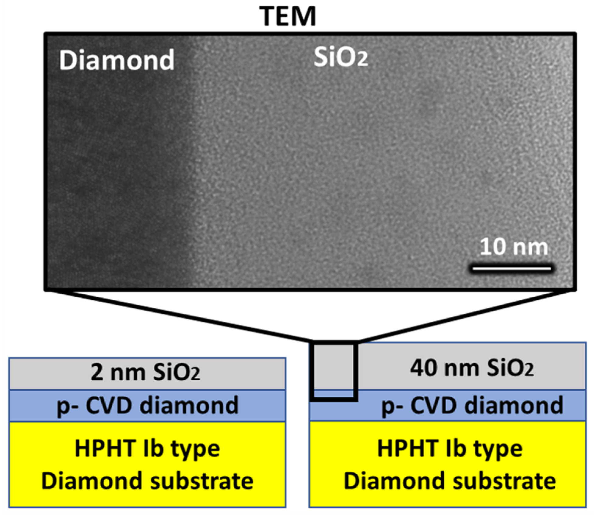
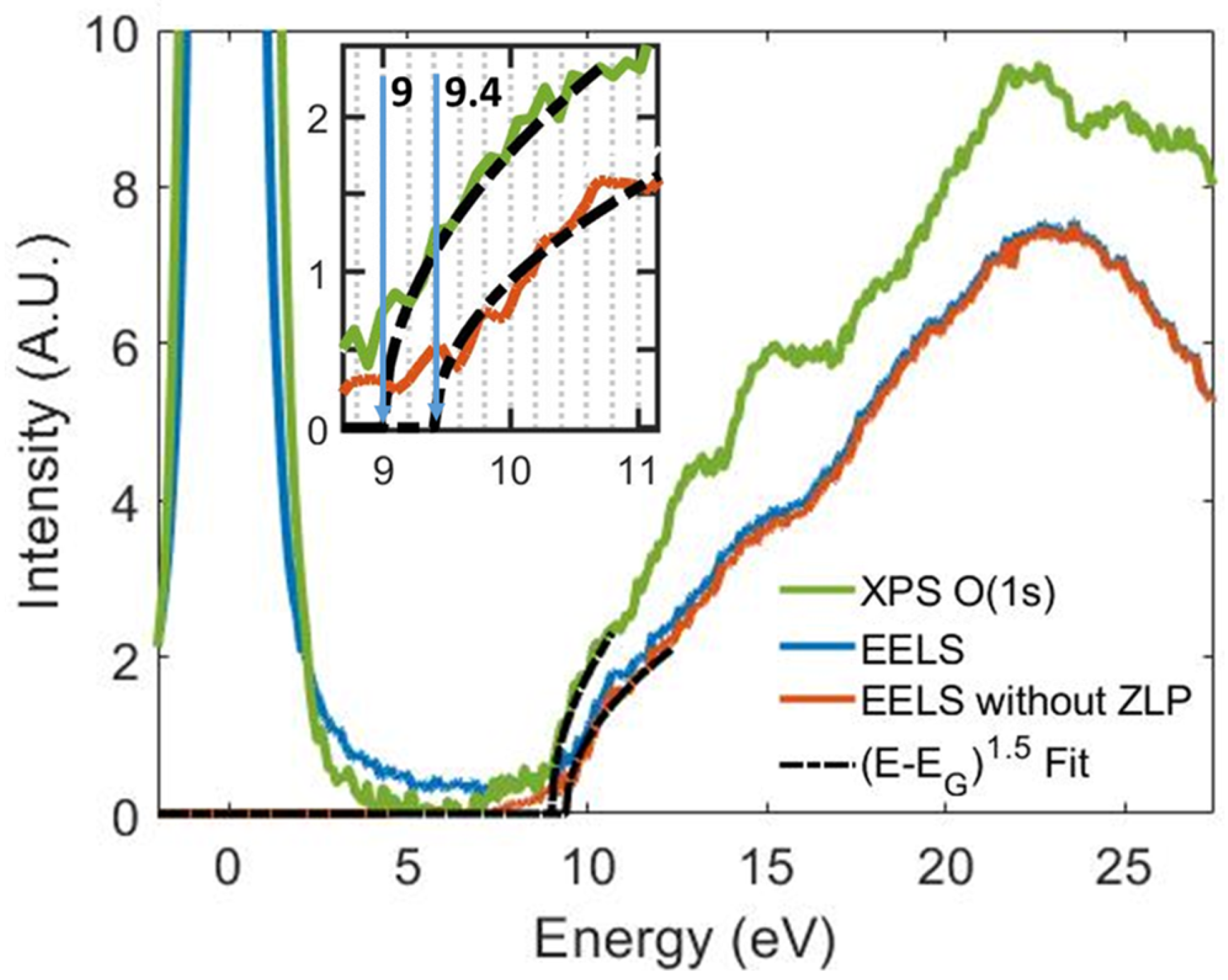
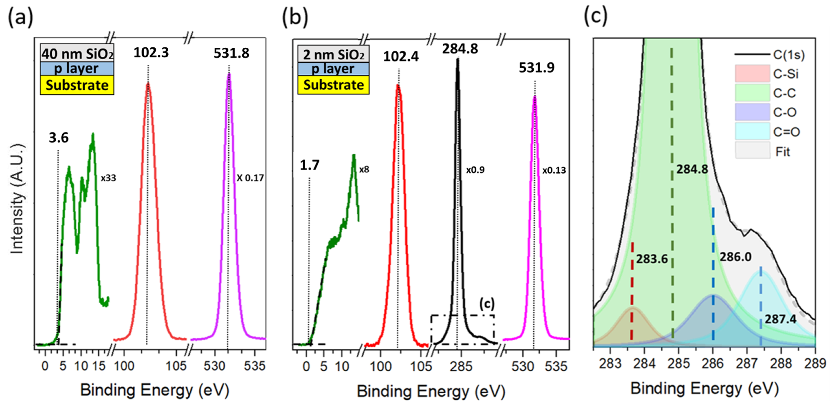
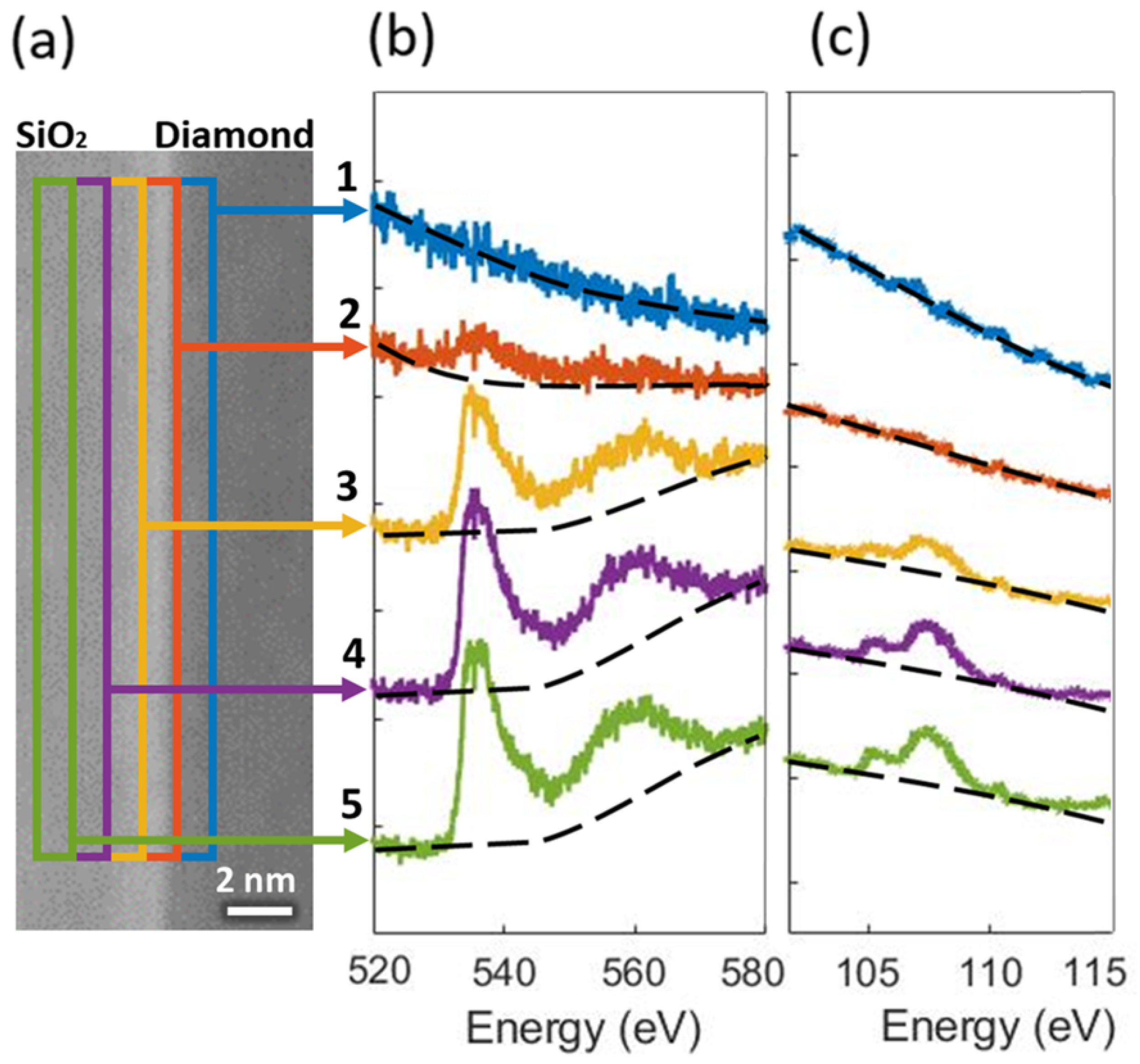
3.1.1. Bulk
3.1.2. Diamond– Interface
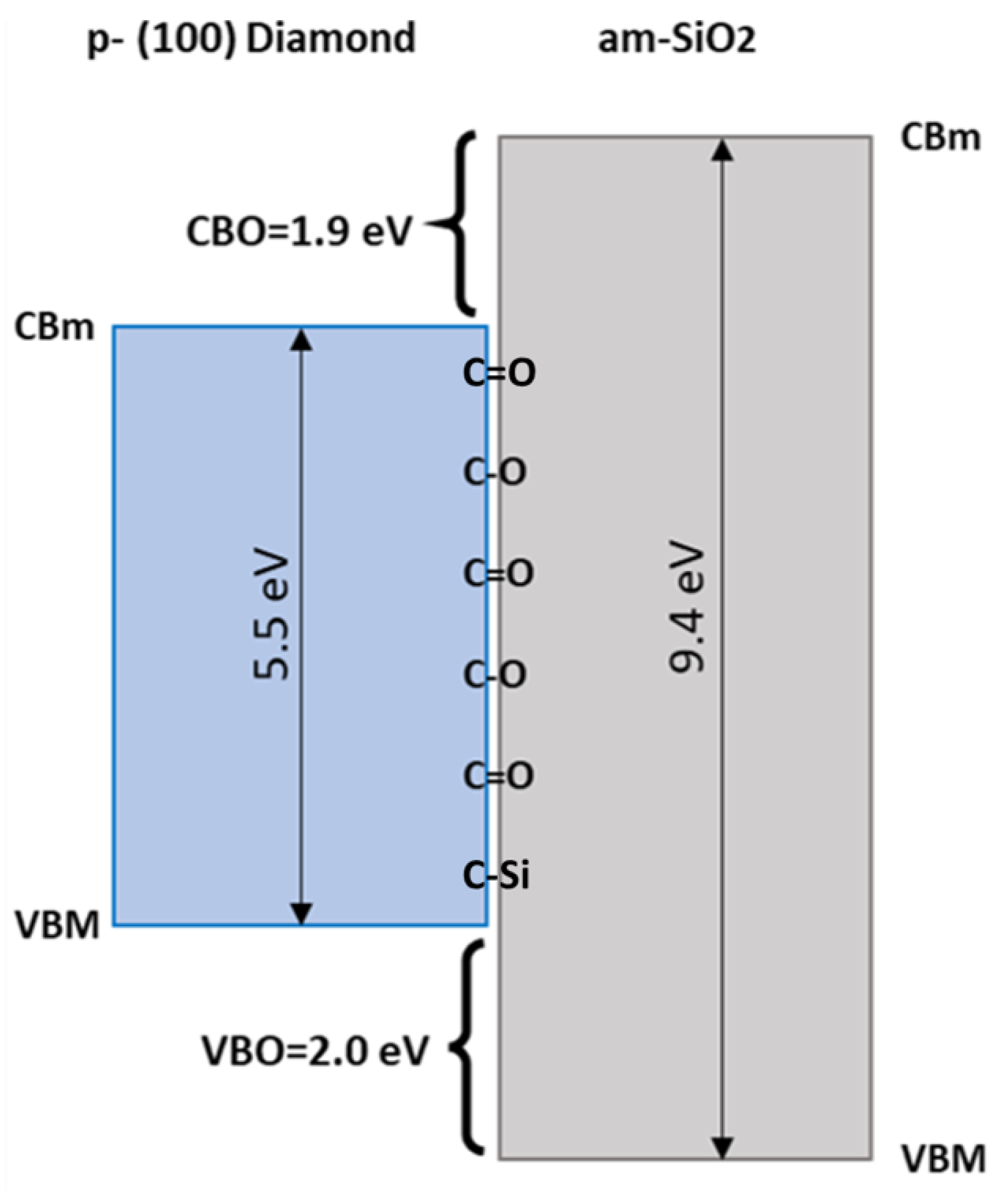
3.1.3. Band Setting
4. Conclusions
Author Contributions
Funding
Data Availability Statement
Acknowledgments
Conflicts of Interest
References
- Hiraiwa, A.; Kawarada, H. Figure of merit of diamond power devices based on accurately estimated impact ionization processes. J. Appl. Phys. 2013, 114, 034506. [Google Scholar] [CrossRef]
- Volpe, P.; Pernot, J.; Muret, P.; Omnès, F. High hole mobility in boron doped diamond for power device applications. Appl. Phys. Lett. 2009, 94, 092102. [Google Scholar] [CrossRef]
- Donato, N.; Rouger, N.; Pernot, J.; Longobardi, G.; Udrea, F. Diamond power devices: State of the art, modelling, figures of merit and future perspective. J. Phys. D Appl. Phys. 2019, 53, 093001. [Google Scholar] [CrossRef] [Green Version]
- Umezawa, H. Recent advances in diamond power semiconductor devices. Mater. Sci. Semicond. Process. 2018, 78, 147–156. [Google Scholar] [CrossRef]
- Araujo, D.; Suzuki, M.; Lloret, F.; Alba, G.; Villar, P. Diamond for Electronics: Materials, Processing and Devices. Materials 2021, 14, 7081. [Google Scholar] [CrossRef] [PubMed]
- Oi, N.; Inaba, M.; Okubo, S.; Tsuyuzaki, I.; Kageura, Y.; Onoda, S.; Hiraiwa, A.; Kawarada, H. Vertical-type two-dimensional hole gas diamond metal oxide semiconductor field-effect transistors. Sci. Rep. 2018, 8, 10660. [Google Scholar] [CrossRef] [Green Version]
- Kitabayashi, Y.; Kudo, T.; Tsuboi, H.; Yamada, T.; Xu, D.; Shibata, M.; Matsumura, D.; Hayashi, Y.; Syamsul, M.; Inaba, M.; et al. Normally-Off C–H Diamond MOSFETs With Partial C–O Channel Achieving 2-kV Breakdown Voltage. IEEE Electron Device Lett. 2017, 38, 363–366. [Google Scholar] [CrossRef]
- Sasama, Y.; Kageura, Y.; Komatsu, K.; Moriyama, S.; Inoue, J.i.; Imura, M.; Watanabe, K.; Taniguchi, T.; Uchihashi, T.; Takahide, Y. Charge-carrier mobility in hydrogen-terminated diamond field-effect transistors. J. Appl. Phys. 2020, 127, 185707. [Google Scholar] [CrossRef]
- Tsunoda, J.; Iwataki, M.; Oi, N.; Morishita, A.; Hiraiwa, A.; Kawarada, H. (111) vertical-type two-dimensional hole gas diamond MOSFETs with hexagonal trench structures. Carbon 2021, 176, 349–357. [Google Scholar] [CrossRef]
- Kawarada, H.; Yamada, T.; Xu, D.; Tsuboi, H.; Kitabayashi, Y.; Matsumura, D.; Shibata, M.; Kudo, T.; Inaba, M.; Hiraiwa, A. Durability-enhanced two-dimensional hole gas of C-H diamond surface for complementary power inverter applications. Sci. Rep. 2017, 7, 42368. [Google Scholar] [CrossRef]
- Zhu, X.; Bi, T.; Yuan, X.; Chang, Y.; Zhang, R.; Fu, Y.; Tu, J.; Huang, Y.; Liu, J.; Li, C.; et al. C-Si interface on SiO2/(111) diamond p-MOSFETs with high mobility and excellent normally off operation. Appl. Surf. Sci. 2022, 593, 153368. [Google Scholar] [CrossRef]
- Umezawa, H.; Matsumoto, T.; Shikata, S.I. Diamond Metal–Semiconductor Field-Effect Transistor with Breakdown Voltage Over 1.5 kV. IEEE Electron Device Lett. 2014, 35, 1112–1114. [Google Scholar] [CrossRef]
- Driche, K. Diamond Unipolar Devices: Towards Impact Ionization Coefficients Extraction. PhD Thesis, Thèse de Doctorat Dirigée par Gheeraert, Etienne Nano Electronique et nano Technologies Université Grenoble Alpes, Grenoble, France, 2018. [Google Scholar]
- Cañas, J.; Pakpour-Tabrizi, A.C.; Trajkovic, T.; Udrea, F.; Eon, D.; Gheeraert, E.; Jackman, R.B. Normally-OFF Diamond Reverse Blocking MESFET. IEEE Trans. Electron Devices 2021, 68, 6279–6285. [Google Scholar] [CrossRef]
- Iwasaki, T.; Yaita, J.; Kato, H.; Makino, T.; Ogura, M.; Takeuchi, D.; Okushi, H.; Yamasaki, S.; Hatano, M. 600 V Diamond Junction Field-Effect Transistors Operated at 200°. IEEE Electron Device Lett. 2013, 35, 241–243. [Google Scholar] [CrossRef]
- Iwasaki, T.; Kato, H.; Makino, T.; Ogura, M.; Takeuchi, D.; Yamasaki, S.; Hatano, M. High-temperature bipolar-mode operation of normally off diamond JFET. IEEE J. Electron Devices Soc. 2016, 5, 95–99. [Google Scholar] [CrossRef]
- Pham, T.T.; Rouger, N.; Masante, C.; Chicot, G.; Udrea, F.; Eon, D.; Gheeraert, E.; Pernot, J. Deep depletion concept for diamond MOSFET. Appl. Phys. Lett. 2017, 111, 173503. [Google Scholar] [CrossRef]
- Pham, T.T.; Pernot, J.; Perez, G.; Eon, D.; Gheeraert, E.; Rouger, N. Deep-Depletion Mode Boron-Doped Monocrystalline Diamond Metal Oxide Semiconductor Field Effect Transistor. IEEE Electron Device Lett. 2017, 38, 1571–1574. [Google Scholar] [CrossRef]
- Pham, T.T.; Pernot, J.; Masante, C.; Eon, D.; Gheeraert, E.; Chicot, G.; Udrea, F.; Rouger, N. 200 V, 4 MV/cm lateral diamond MOSFET. In Proceedings of the 2017 IEEE International Electron Devices Meeting (IEDM), San Francisco, CA, USA, 2–6 December 2017; pp. 25.4.1–25.4.4. [Google Scholar] [CrossRef]
- Masante, C.; Pernot, J.; Letellier, J.; Eon, D.; Rouger, N. 175 V, >5.4 MV/cm, 50 mΩm.cm2 at 250 °C Diamond MOSFET and its reverse conduction. In Proceedings of the 2019 31st International Symposium on Power Semiconductor Devices and ICs (ISPSD), Shanghai, China, 19–23 May 2019; pp. 151–154. [Google Scholar] [CrossRef]
- Umezawa, H.; Ohmagari, S.; Mokuno, Y.; Kaneko, J.H. Characterization of X-ray radiation hardness of diamond Schottky barrier diode and metal-semiconductor field-effect transistor. In Proceedings of the 2017 29th International Symposium on Power Semiconductor Devices and IC’s (ISPSD), Sapporo, Japan, 28 May–1 June 2017; pp. 379–382. [Google Scholar] [CrossRef]
- Matsumoto, T.; Kato, H.; Oyama, K.; Makino, T.; Ogura, M.; Takeuchi, D.; Inokuma, T.; Tokuda, N.; Yamasaki, S. Inversion channel diamond metal-oxide-semiconductor field-effect transistor with normally off characteristics. Sci. Rep. 2016, 6, 31585. [Google Scholar] [CrossRef]
- Rutter, M.J.; Robertson, J. Ab initio calculation of electron affinities of diamond surfaces. Phys. Rev. B 1998, 57, 9241–9245. [Google Scholar] [CrossRef]
- Navas, J.; Araujo, D.; Piñero, J.C.; Sánchez-Coronilla, A.; Blanco, E.; Villar, P.; Alcántara, R.; Montserrat, J.; Florentin, M.; Eon, D.; et al. Oxygen termination of homoepitaxial diamond surface by ozone and chemical methods: An experimental and theoretical perspective. Appl. Surf. Sci. 2018, 433, 408–418. [Google Scholar] [CrossRef]
- Teraji, T.; Koide, Y.; Ito, T. Schottky barrier height and thermal stability of p-diamond (100) Schottky interfaces. Thin Solid Films 2014, 557, 241–248. [Google Scholar] [CrossRef]
- Chicot, G.; Maréchal, A.; Motte, R.; Muret, P.; Gheeraert, E.; Pernot, J. Metal oxide semiconductor structure using oxygen-terminated diamond. Appl. Phys. Lett. 2013, 102, 242108. [Google Scholar] [CrossRef] [Green Version]
- Loto, O.; Florentin, M.; Masante, C.; Donato, N.; Hicks, M.L.; Pakpour-Tabrizi, A.C.; Jackman, R.B.; Zuerbig, V.; Godignon, P.; Eon, D.; et al. Gate Oxide Electrical Stability of p-type Diamond MOS Capacitors. IEEE Trans. Electron Devices 2018, 65, 3361–3364. [Google Scholar] [CrossRef] [Green Version]
- Pham, T.T.; Maréchal, A.; Muret, P.; Eon, D.; Gheeraert, E.; Rouger, N.; Pernot, J. Comprehensive electrical analysis of metal/Al2O3/O-terminated diamond capacitance. J. Appl. Phys. 2018, 123, 161523. [Google Scholar] [CrossRef]
- Soto, B.; Cañas, J.; Villar, M.; Araujo, D.; Pernot, J. Transport mechanism in O-terminated diamond/ZrO2 based MOSCAPs. Diam. Relat. Mater. 2021, 121, 108745. [Google Scholar] [CrossRef]
- Kovi, K.K.; Vallin, Ö.; Majdi, S.; Isberg, J. Inversion in Metal–Oxide–Semiconductor Capacitors on Boron-Doped Diamond. IEEE Electron Device Lett. 2015, 36, 603–605. [Google Scholar] [CrossRef]
- Cañas, J.; Piñero, J.; Lloret, F.; Gutierrez, M.; Pham, T.; Pernot, J.; Araujo, D. Determination of alumina bandgap and dielectric functions of diamond MOS by STEM-VEELS. Appl. Surf. Sci. 2018, 461, 93–97. [Google Scholar] [CrossRef]
- Cañas, J.; Alba, G.; Leinen, D.; Lloret, F.; Gutierrez, M.; Eon, D.; Pernot, J.; Gheeraert, E.; Araujo, D. Diamond/γ-alumina band offset determination by XPS. Appl. Surf. Sci. 2021, 535, 146301. [Google Scholar] [CrossRef]
- Cañas, J.; Dussarrat, C.; Teramoto, T.; Masante, C.; Gutierrez, M.; Gheeraert, E. High quality SiO2/diamond interface in O-terminated p-type diamond MOS capacitors. Appl. Phys. Lett. 2022, 121, 072101. [Google Scholar] [CrossRef]
- Huang, B.; Bai, X.; Lam, S.K.; Tsang, K.K. Diamond FinFET without Hydrogen Termination. Sci. Rep. 2018, 8, 3063. [Google Scholar] [CrossRef] [Green Version]
- Fei, W.; Bi, T.; Iwataki, M.; Imanishi, S.; Kawarada, H. Publisher’s Note: “Oxidized Si terminated diamond and its MOSFET operation with SiO2 gate insulator”. Appl. Phys. Lett. 2020, 116, 269901. [Google Scholar] [CrossRef]
- Stöger-Pollach, M.; Franco, H.; Schattschneider, P.; Lazar, S.; Schaffer, B.; Grogger, W.; Zandbergen, H. Čerenkov losses: A limit for bandgap determination and Kramers–Kronig analysis. Micron 2006, 37, 396–402. [Google Scholar] [CrossRef]
- Stöger-Pollach, M.; Schattschneider, P. The influence of relativistic energy losses on bandgap determination using valence EELS. Ultramicroscopy 2007, 107, 1178–1185. [Google Scholar] [CrossRef]
- Kimoto, K.; Kothleitner, G.; Grogger, W.; Matsui, Y.; Hofer, F. Advantages of a monochromator for bandgap measurements using electron energy-loss spectroscopy. Micron 2005, 36, 185–189. [Google Scholar] [CrossRef]
- Maréchal, A.; Aoukar, M.; Vallée, C.; Rivière, C.; Eon, D.; Pernot, J.; Gheeraert, E. Energy-band diagram configuration of Al2O3/oxygen-terminated p-diamond metal-oxide-semiconductor. Appl. Phys. Lett. 2015, 107, 141601. [Google Scholar] [CrossRef]
- Maréchal, A.; Kato, Y.; Liao, M.; Koizumi, S. Interfacial energy barrier height of Al2O3/H-terminated (111) diamond heterointerface investigated by X-ray photoelectron spectroscopy. Appl. Phys. Lett. 2017, 111, 141605. [Google Scholar] [CrossRef] [Green Version]
- Liu, J.W.; Liao, M.Y.; Imura, M.; Koide, Y. Band offsets of Al2O3 and HfO2 oxides deposited by atomic layer deposition technique on hydrogenated diamond. Appl. Phys. Lett. 2012, 101, 252108. [Google Scholar] [CrossRef]
- Zhang, F.; Sun, G.; Zheng, L.; Liu, S.; Liu, B.; Dong, L.; Wang, L.; Zhao, W.; Liu, X.; Yan, G.; et al. Interfacial study and energy-band alignment of annealed Al2O3 films prepared by atomic layer deposition on 4H-SiC. J. Appl. Phys. 2013, 113, 044112. [Google Scholar] [CrossRef]
- Ren, Z.; Lv, D.; Xu, J.; Zhang, J.; Zhang, J.; Su, K.; Zhang, C.; Hao, Y. High temperature (300 °C) ALD grown Al2O3 on hydrogen terminated diamond: Band offset and electrical properties of the MOSFETs. Appl. Phys. Lett. 2020, 116, 013503. [Google Scholar] [CrossRef]
- Takahashi, K.; Imamura, M.; Hirama, K.; Kasu, M. Electronic states of NO2-exposed H-terminated diamond/Al2O3 heterointerface studied by synchrotron radiation photoemission and X-ray absorption spectroscopy. Appl. Phys. Lett. 2014, 104, 072101. [Google Scholar] [CrossRef]
- Teraji, T.; Garino, Y.; Koide, Y.; Ito, T. Low-leakage p-type diamond Schottky diodes prepared using vacuum ultraviolet light/ozone treatment. J. Appl. Phys. 2009, 105, 126109. [Google Scholar] [CrossRef]
- Tougaard, S.; Sigmund, P. Influence of elastic and inelastic scattering on energy spectra of electrons emitted from solids. Phys. Rev. B 1982, 25, 4452–4466. [Google Scholar] [CrossRef]
- Garvie, L.; Rez, P.; Alvarez, J.; Buseck, P. Interband transitions of crystalline and amorphous SiO2: An electron energy-loss spectroscopy (EELS) study of the low-loss region. Solid State Commun. 1998, 106, 303–307. [Google Scholar] [CrossRef]
- Weinberg, Z.A.; Rubloff, G.W.; Bassous, E. Transmission, photoconductivity, and the experimental band gap of thermally grown SiO2 films. Phys. Rev. B 1979, 19, 3107–3117. [Google Scholar] [CrossRef]
- Shinotsuka, H.; Tanuma, S.; Powell, C.J.; Penn, D.R. Calculations of electron inelastic mean free paths. X. Data for 41 elemental solids over the 50 eV to 200 keV range with the relativistic full Penn algorithm. Surf. Interface Anal. 2015, 47, 871–888. [Google Scholar] [CrossRef]
- Koh, D.; Banerjee, S.; Brockman, J.; Kuhn, M.; King, S.W. X-ray photoelectron spectroscopy investigation of the valence band offset at beryllium oxide-diamond interfaces. Diam. Relat. Mater. 2020, 101, 107647. [Google Scholar] [CrossRef]
- Donato, N. Modelling and Design of Diamond Power Semiconductor Devices. PhD Thesis, University of Cambridge, Cambridge, UK, 2019. [Google Scholar]
- Tung, R.T.; Kronik, L. Charge Density and Band Offsets at Heterovalent Semiconductor Interfaces. Adv. Theory Simul. 2018, 1, 1700001. [Google Scholar] [CrossRef]


| Spectrum | 2 nm | 40 nm | |
| VBM | Energy | 1.7 eV | 3.6 eV |
| Si(2p) | Energy | 102.4 eV | 102.3 eV |
| FWHM | 1.7 eV | 1.6 eV | |
| O(1s) | Energy | 531.9 eV | 531.8 eV |
| FWHM | 1.6 eV | 1.5 eV | |
| Energy | 284.8 eV | - | |
| FWHM | 0.7 eV | - | |
| C(1s) interfacial component | Energy | Relative area | |
| 283.6 eV | 15% | ||
| 286.0 eV | 35% | ||
| 287.4 eV | 50% | ||
Publisher’s Note: MDPI stays neutral with regard to jurisdictional claims in published maps and institutional affiliations. |
© 2022 by the authors. Licensee MDPI, Basel, Switzerland. This article is an open access article distributed under the terms and conditions of the Creative Commons Attribution (CC BY) license (https://creativecommons.org/licenses/by/4.0/).
Share and Cite
Cañas, J.; Reyes, D.F.; Zakhtser, A.; Dussarrat, C.; Teramoto, T.; Gutiérrez, M.; Gheeraert, E. High-Quality SiO2/O-Terminated Diamond Interface: Band-Gap, Band-Offset and Interfacial Chemistry. Nanomaterials 2022, 12, 4125. https://doi.org/10.3390/nano12234125
Cañas J, Reyes DF, Zakhtser A, Dussarrat C, Teramoto T, Gutiérrez M, Gheeraert E. High-Quality SiO2/O-Terminated Diamond Interface: Band-Gap, Band-Offset and Interfacial Chemistry. Nanomaterials. 2022; 12(23):4125. https://doi.org/10.3390/nano12234125
Chicago/Turabian StyleCañas, Jesús, Daniel F. Reyes, Alter Zakhtser, Christian Dussarrat, Takashi Teramoto, Marina Gutiérrez, and Etienne Gheeraert. 2022. "High-Quality SiO2/O-Terminated Diamond Interface: Band-Gap, Band-Offset and Interfacial Chemistry" Nanomaterials 12, no. 23: 4125. https://doi.org/10.3390/nano12234125