
Nanoscale Printing of Indium-Tin-Oxide by Femtosecond Laser Pulses
 , and
, and 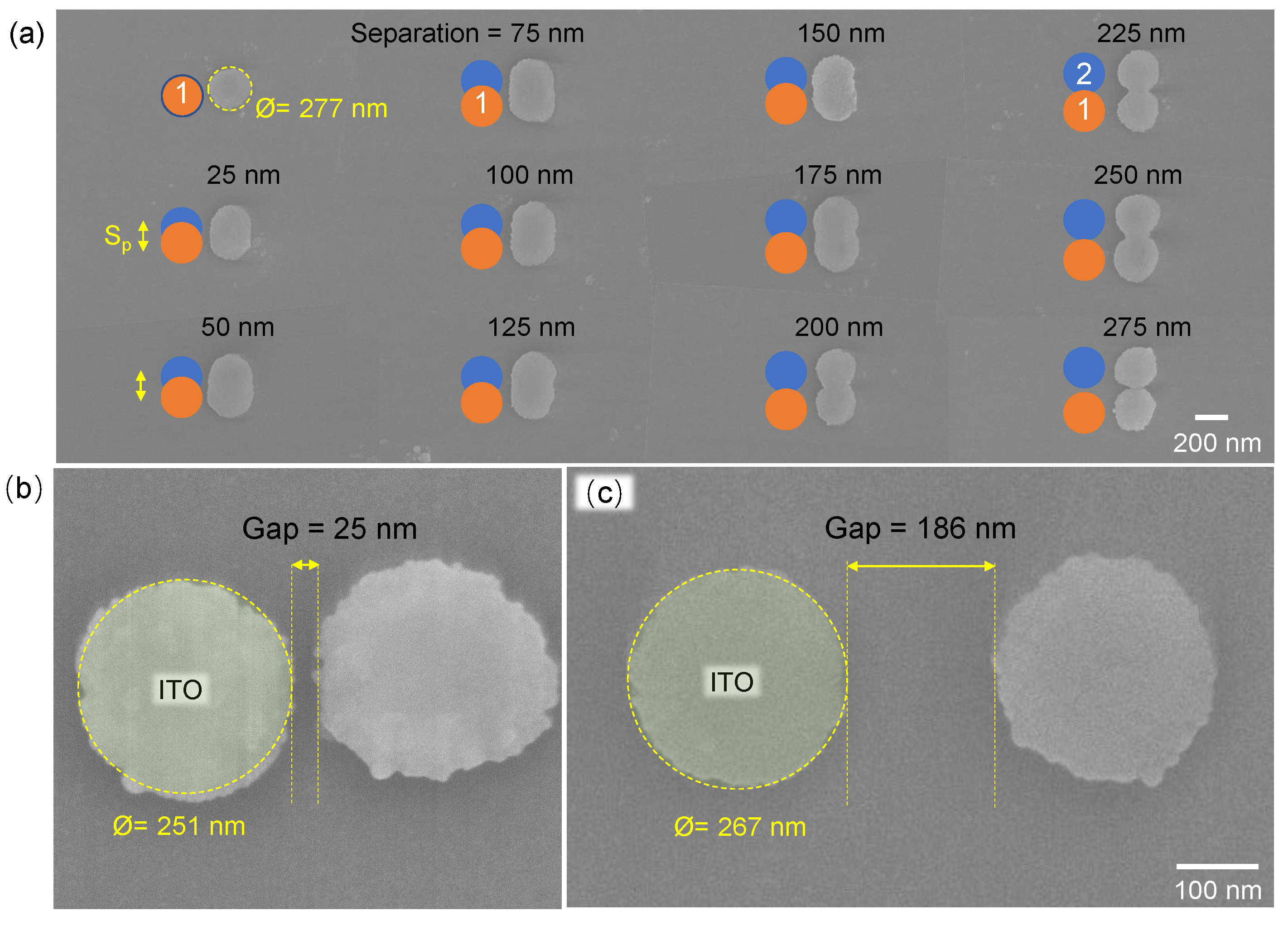
Abstract
:1. Introduction
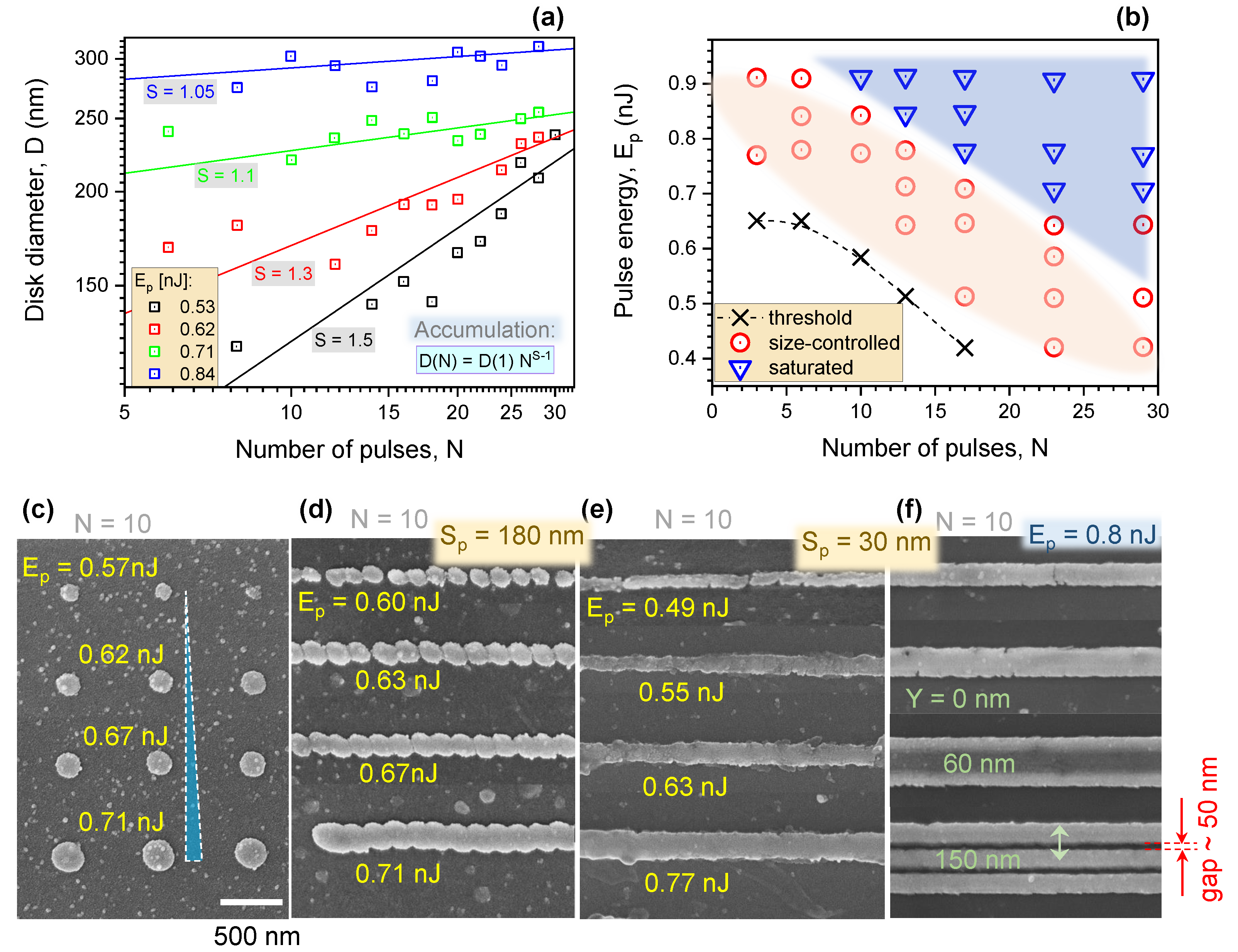
2. Results and Discussion
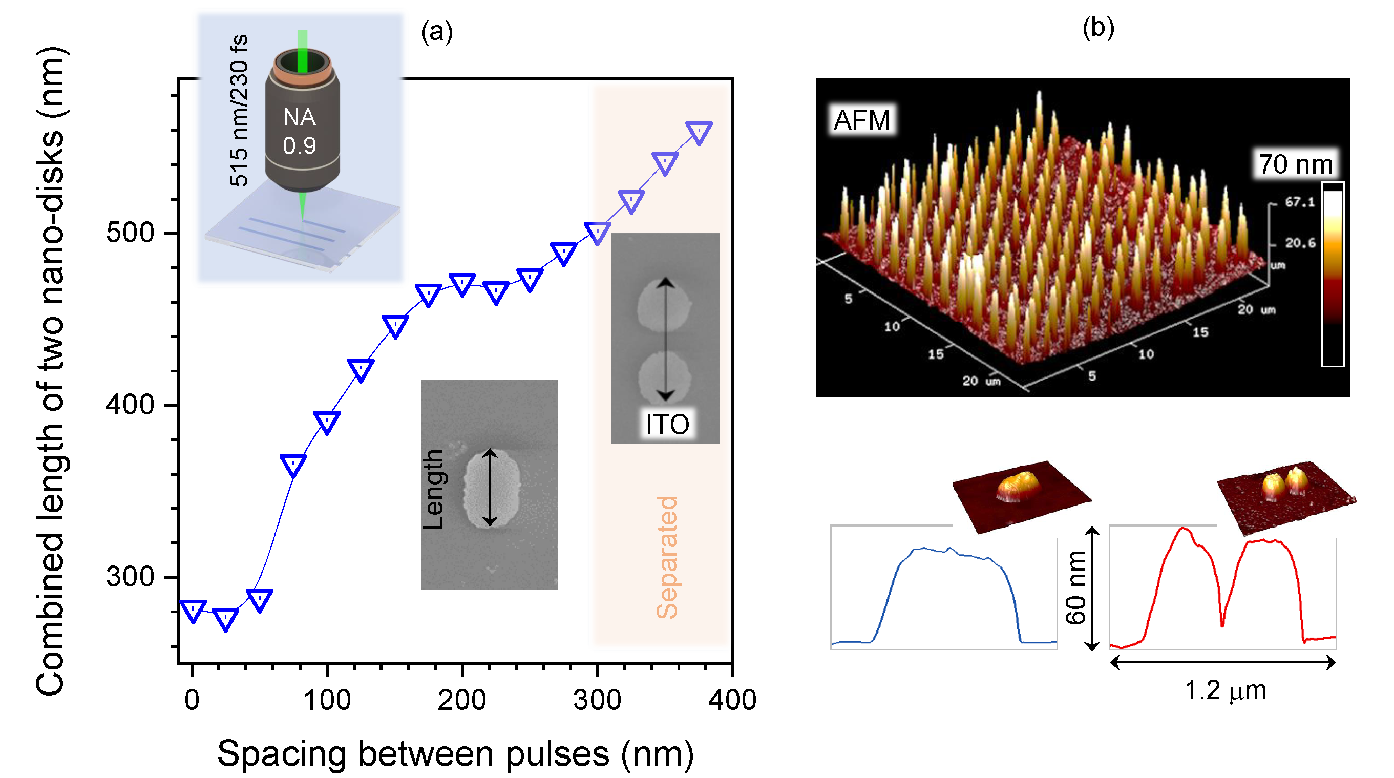
2.1. Single Nano-Disks and Pairs
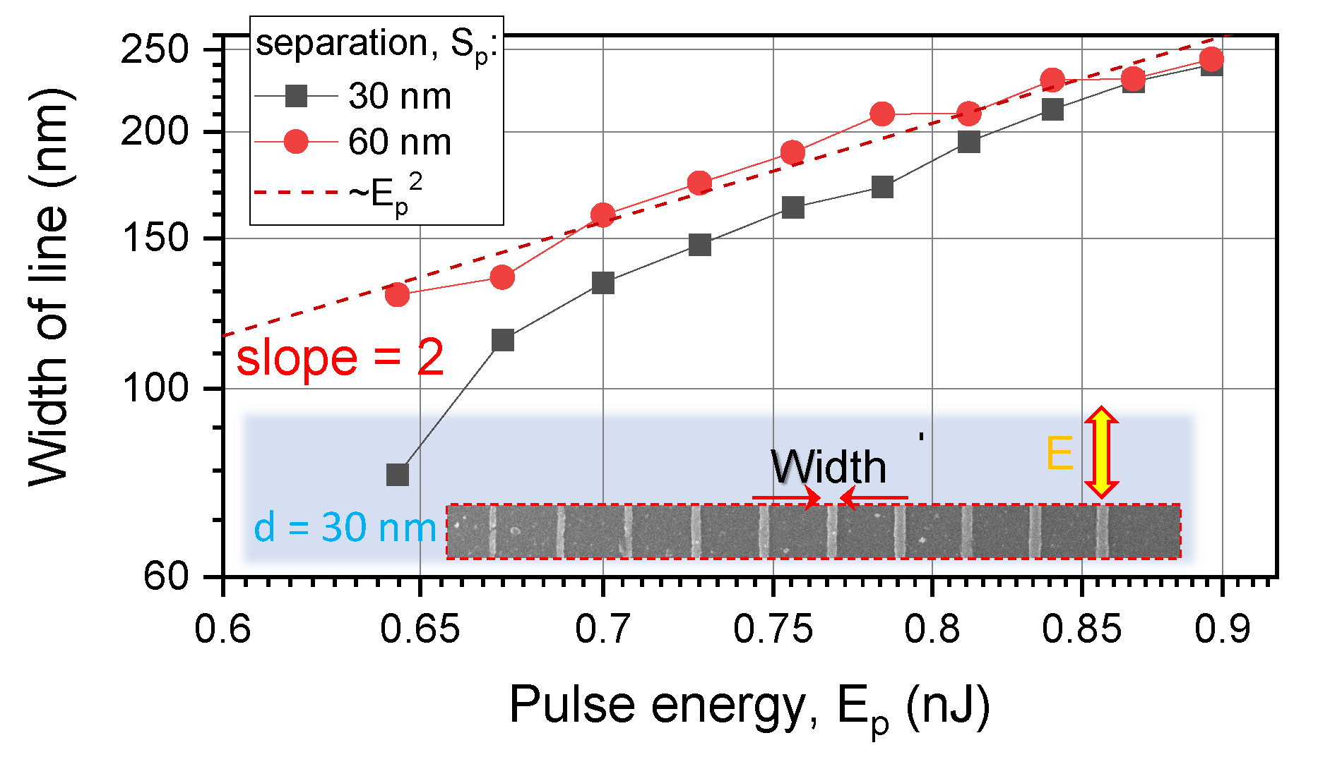
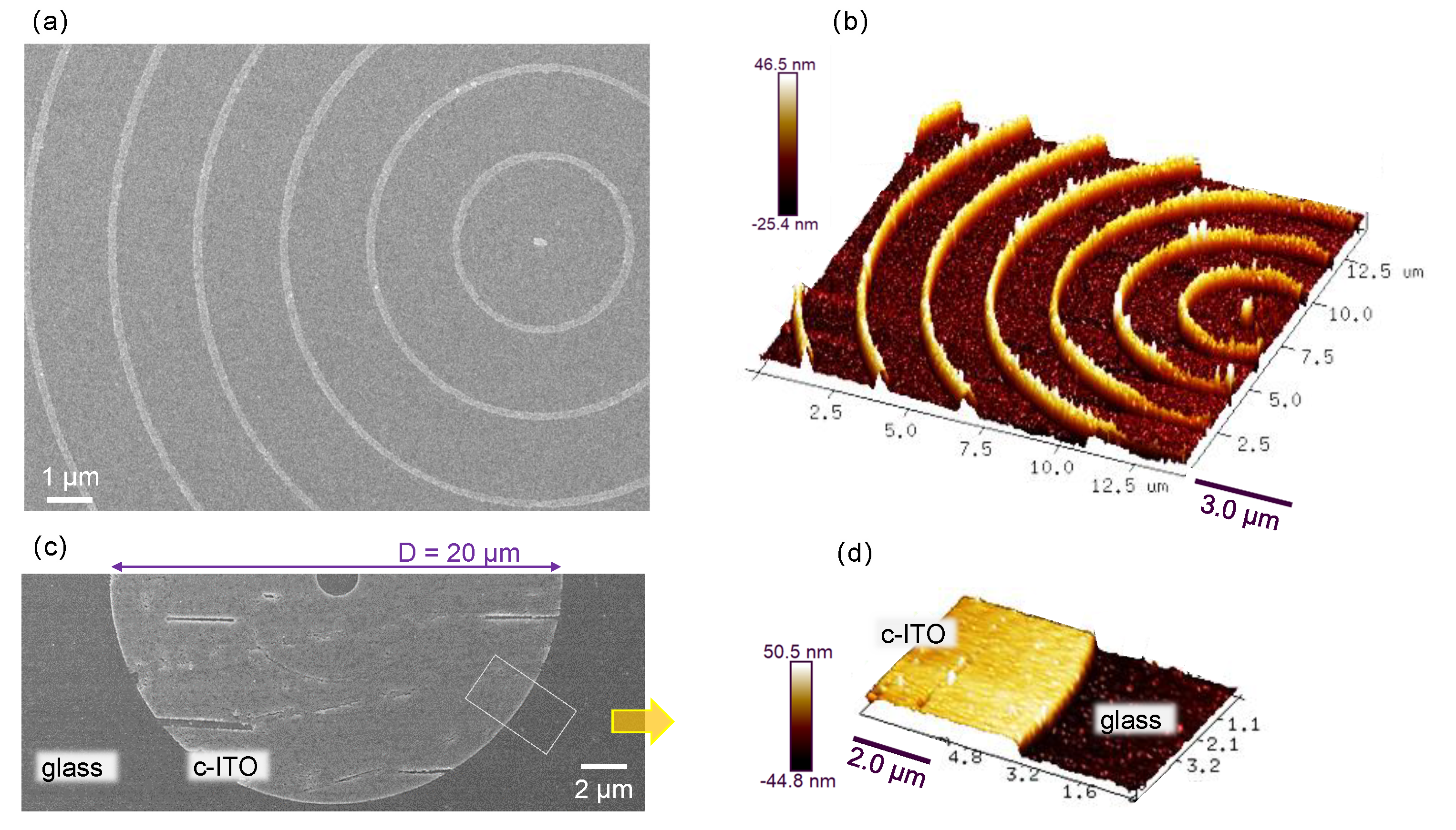
2.2. From Lines with Nano-Gaps to Optical Micro-Elements
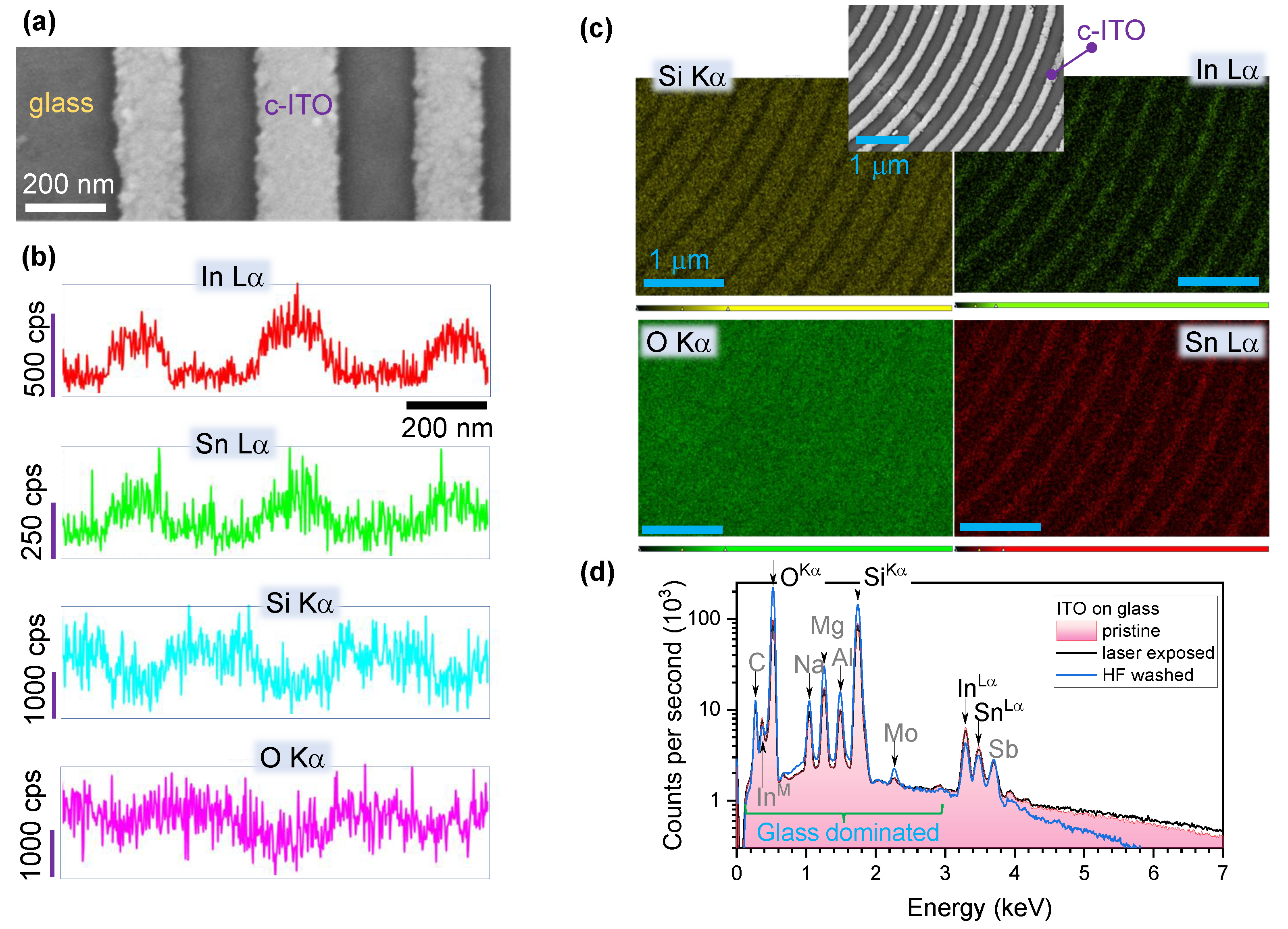
2.3. Material Analysis
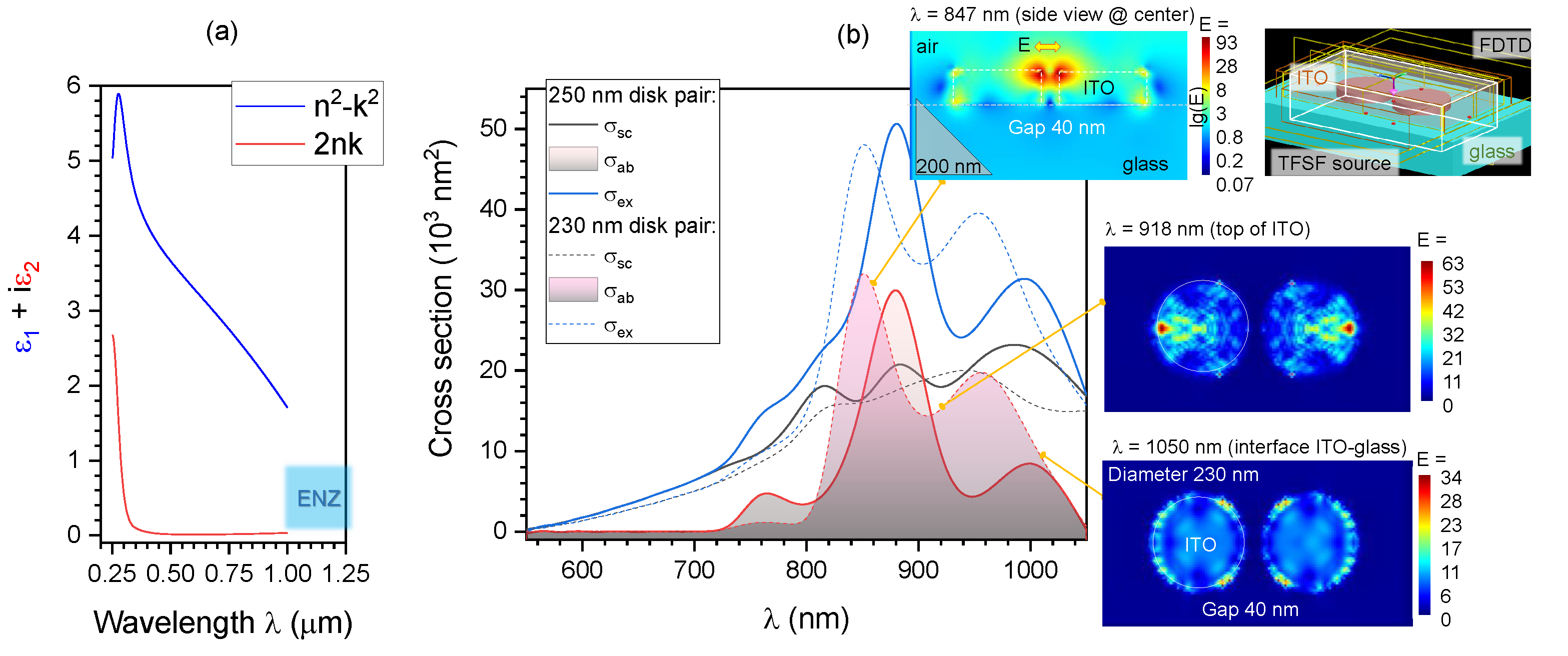
2.4. Numerical Modeling of Light Field Enhancement
3. Conclusions and Outlook
4. Experimental: Samples and Procedures
Author Contributions
Funding
Data Availability Statement
Acknowledgments
Conflicts of Interest
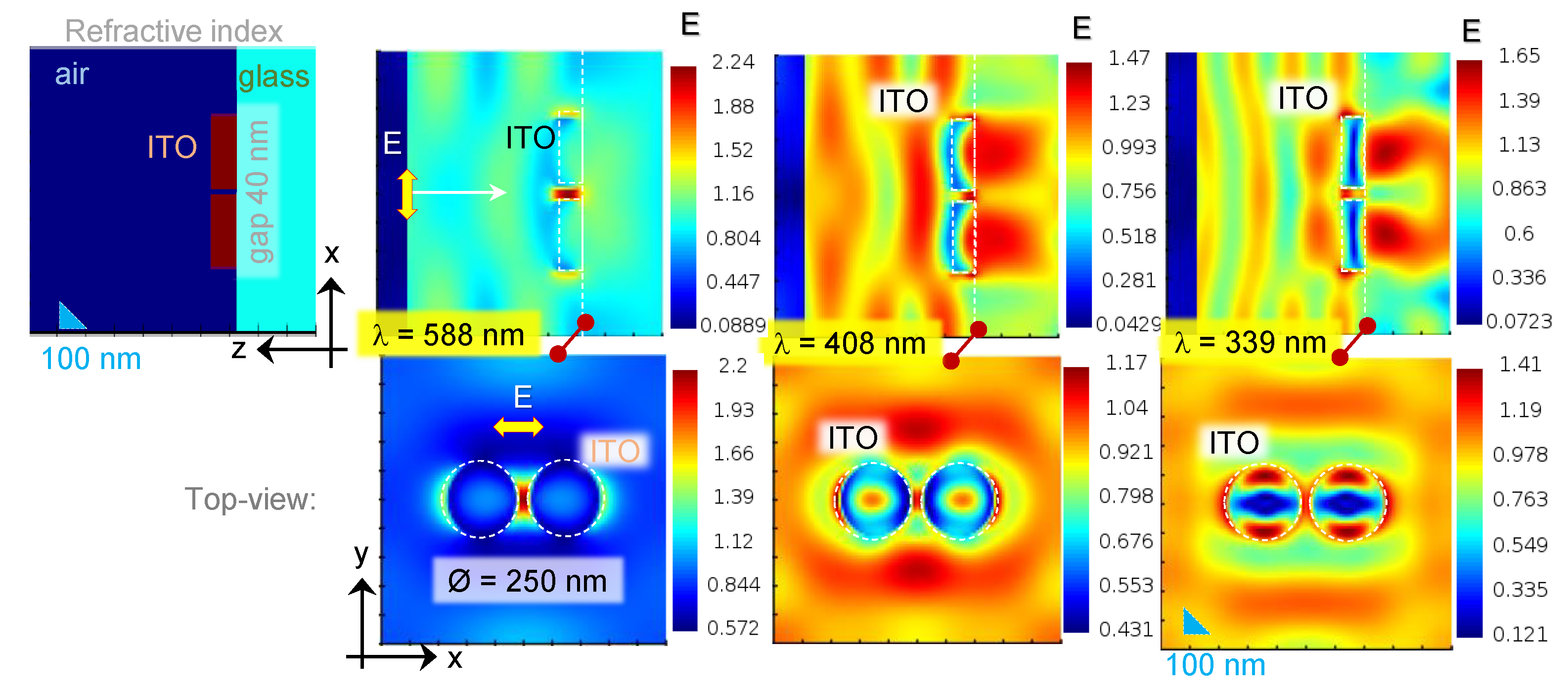
Appendix A. Additional Simulations

References
- Ray, S.; Banerjee, R.; Basu, N.; Batabyal, A.K.; Barua, A.K. Properties of tin doped indium oxide thin films prepared by magnetron sputtering. J. Appl. Phys. 1983, 54, 3497–3501. [Google Scholar] [CrossRef]
- Hamberg, I.; Granqvist, C.G. Evaporated Sn-doped In2O3films: Basic optical properties and applications to energy-efficient windows. J. Appl. Phys. 1986, 60, R123–R160. [Google Scholar] [CrossRef]
- Baum, M.; Alexeev, I.; Latzel, M.; Christiansen, S.H.; Schmidt, M. Determination of the effective refractive index of nanoparticulate ITO layers. Opt. Express 2013, 21, 22754–22761. [Google Scholar] [CrossRef] [PubMed] [Green Version]
- Nadaud, N.; Lequeux, N.; Nanot, M.; Jové, J.; Roisnel, T. Structural Studies of Tin-Doped Indium Oxide (ITO) and In4Sn3O12. J. Solid State Chem. 1998, 135, 140–148. [Google Scholar] [CrossRef] [Green Version]
- Ishibashi, S.; Higuchi, Y.; Ota, Y.; Nakamura, K. Low resistivity indium–tin oxide transparent conductive films. II. Effect of sputtering voltage on electrical property of films. J. Vac. Sci. Technol. Vacuum Surfaces Film. 1990, 8, 1403–1406. [Google Scholar] [CrossRef]
- Ma, Z.; Li, Z.; Liu, K.; Ye, C.; Sorger, V.J. Indium-Tin-Oxide for High-performance Electro-optic Modulation. Nanophotonics 2015, 4, 198–213. [Google Scholar] [CrossRef]
- Kim, Y.N.; Jeong, S.M.; Jeon, M.S.; Shin, H.; Song, J.K.; Lee, H. Reliability assessment of indium tin oxide thin films by accelerated degradation test. J. Electroceramics 2006, 17, 955–958. [Google Scholar] [CrossRef]
- Yu, Z.; Perera, I.; Daeneke, T.; Makuta, S.; Tachibana, Y.; Jasieniak, J.; Mishra, A.; Bäuerle, P.; Spiccia, L.; Bach, U. Indium tin oxide as a semiconductor material in efficient p-type dye-sensitized solar cells. NPG Asia Mater. 2016, 8, 305. [Google Scholar] [CrossRef]
- Paine, D.C.; Whitson, T.; Janiac, D.; Beresford, R.; Yang, C.O.; Lewis, B. A study of low temperature crystallization of amorphous thin film indium–tin–oxide. J. Appl. Phys. 1999, 85, 8445–8450. [Google Scholar] [CrossRef]
- Xian, S.; Nie, L.; Qin, J.; Kang, T.; Li, C.; Xie, J.; Deng, L.; Bi, L. Effect of oxygen stoichiometry on the structure, optical and epsilon-near-zero properties of indium tin oxide films. Opt. Express 2019, 27, 28618–28628. [Google Scholar] [CrossRef]
- Alam, M.Z.; De Leon, I.; Boyd, R.W. Large optical nonlinearity of indium tin oxide in its epsilon-near-zero region. J. Electroceramics 2016, 352, 795–797. [Google Scholar] [CrossRef] [PubMed]
- Guo, P.; Schaller, R.D.; Ocola, L.E.; Diroll, B.T.; Ketterson, J.B.; Chang, R. Large optical nonlinearity of ITO nanorods for sub-picosecond all-optical modulation of the full-visible spectrum. Nat. Commun. 2016, 7, 12892. [Google Scholar] [CrossRef] [PubMed] [Green Version]
- Ng, S.N.; Juodkazis, S. Nanoscale Plasmonic Printing. Preprints 2022, 2022020258. [Google Scholar] [CrossRef]
- Lai, S.; Guo, Y.; Liu, G.; Liu, Y.; Fu, C.; Chang, H.; Wu, Y.; Gu, W. A High-Performance Ultra-Broadband Transparent Absorber With a Patterned ITO Metasurface. IEEE Photonics J. 2022, 14, 1–7. [Google Scholar] [CrossRef]
- Forouzmand, A.; Salary, M.M.; Kafaie Shirmanesh, G.; Sokhoyan, R.; Atwater, H.A.; Mosallaei, H. Tunable all-dielectric metasurface for phase modulation of the reflected and transmitted light via permittivity tuning of indium tin oxide. Nanophotonics 2019, 8, 415–427. [Google Scholar] [CrossRef]
- Ni, J.H.; Sarney, W.L.; Leff, A.C.; Cahill, J.P.; Zhou, W. Property Variation in Wavelength-thick Epsilon-Near-Zero ITO Metafilm for Near IR Photonic Devices. Sci. Rep. 2020, 10, 713. [Google Scholar] [CrossRef] [Green Version]
- Datta, R.; Syed, N.; Zavabeti, A.; Jannat, A.; Mohiuddin, M.; Rokunuzzaman, M.; Zhang, B.; Ataur Rahman, M.; Atkin, P.; Messalea, K.; et al. Flexible two-dimensional indium tin oxide fabricated using a liquid metal printing technique. Nat. Electron. 2020, 3, 51–58. [Google Scholar] [CrossRef]
- Allioux, F.M.; Ghasemian, M.; Xie, W.; O’Mullane, A.; Daeneke, T.; Dickey, M.; Kalantar-Zadeh, K. Applications of liquid metals in nanotechnology. Nanoscale Horiz. 2022, 7, 141–167. [Google Scholar] [CrossRef]
- Patel, N.; Patel, P.; Vaishnav, V. Indium tin oxide (ITO) thin film gas sensor for detection of methanol at room temperature. Sens. Actuators Chem. 2003, 96, 180–189. [Google Scholar] [CrossRef]
- Görrn, P.; Sander, M.; Meyer, J.; Kröger, M.; Becker, E.; Johannes, H.; Kowalsky, W.; Riedl, T. Towards see-through displays: Fully transparent thin-film transistors driving transparent organic light-emitting diodes. Adv. Mater. 2006, 18, 738–741. [Google Scholar] [CrossRef]
- Morikawa, H.; Fujita, M. Crystallization and electrical property change on the annealing of amorphous indium-oxide and indium-tin-oxide thin films. Thin Solid Film. 2000, 359, 61–67. [Google Scholar]
- Afshar, M.; Straub, M.; Voellm, H.; Feili, D.; Koenig, K.; Seidel, H. Sub-100 nm structuring of indium-tin-oxide thin films by sub-15 femtosecond pulsed near-infrared laser light. Opt. Lett. 2012, 37, 563–565. [Google Scholar] [CrossRef] [PubMed]
- Cheng, C.W.; Lin, C.Y. High precision patterning of ITO using femtosecond laser annealing process. Appl. Surf. Sci. 2014, 314, 215–220. [Google Scholar] [CrossRef]
- Cheng, C.W.; Lin, C.Y.; Shen, W.C.; Lee, Y.J.; Chen, J.S. Patterning crystalline indium tin oxide by high repetition rate femtosecond laser-induced crystallization. Thin Solid Film. 2010, 518, 7138–7142. [Google Scholar] [CrossRef]
- Farid, N.; Dasgupta, P.; O’Connor, G. Onset and evolution of laser induced periodic surface structures on indium tin oxide thin films for clean ablation using a repetitively pulsed picosecond laser at low fluence. J. Phys. Appl. Phys. 2018, 51, 155104. [Google Scholar]
- Cerkauskaite, A.; Drevinskas, R.; Solodar, A.; Abdulhalim, I.; Kazansky, P.G. Form-Birefringence in ITO Thin Films Engineered by Ultrafast Laser Nanostructuring. ACS Photonics 2017, 4, 2944–2951. [Google Scholar] [CrossRef]
- Cheng, C.W.; Lee, I.M.; Chen, J.S. Femtosecond laser-induced nanoperiodic structures and simultaneous crystallization in amorphous indium-tin-oxide thin films. Appl. Surf. Sci. 2014, 316, 9–14. [Google Scholar] [CrossRef]
- Li, Z.H.; Cho, E.S.; Kwon, S.J. A new laser direct etching method of indium tin oxide electrode for application to alternative current plasma display panel. Appl. Surf. Sci. 2009, 255, 9843–9846. [Google Scholar] [CrossRef]
- Chae, J.; Jang, L.; Jain, K. High-resolution, resistless patterning of indium-tin-oxide thin films using excimer laser projection annealing process. Mater. Lett. 2010, 64, 948–950. [Google Scholar] [CrossRef]
- Lee, C.J.; Lin, H.K.; Li, C.H.; Chen, L.X.; Lee, C.C.; Wu, C.W.; Huang, J.C. A study on electric properties for pulse laser annealing of ITO film after wet etching. Thin Solid Film. 2012, 522, 330–335. [Google Scholar] [CrossRef]
- Legeay, G.; Castel, X.; Benzerga, R.; Pinel, J. Excimer laser beam/ITO interaction: From laser processing to surface reaction. Phys. Status Solidi C 2008, 5, 3248–3254. [Google Scholar] [CrossRef]
- Hosono, H.; Kurita, M.; Kawazoe, H. Excimer laser crystallization of amorphous indium-tin-oxide and its application to fine patterning. Jpn. J. Appl. Phys. Part Lett. 1998, 37, 8–11. [Google Scholar] [CrossRef]
- Su, S.H.; Kong, H.J.; Tseng, C.L.; Chen, G.Y. Wet etching mechanism and crystallization of indium-tin oxide layer for application in light-emitting diodes. Jpn. J. Appl. Phys. 2018, 57, 1–5. [Google Scholar] [CrossRef]
- Wang, S.; Zhou, Z.; Li, B.; Wang, C.; Liu, Q. Progresses on new generation laser direct writing technique. Mater. Today Nano 2021, 16, 100142. [Google Scholar] [CrossRef]
- Li, Z.Z.; Wang, L.; Fan, H.; Yu, Y.H.; Chen, Q.D.; Juodkazis, S.; Sun, H.B. O-FIB: Far-field-induced near-field breakdown for direct nanowriting in an atmospheric environment. Light Sci. Appl. 2020, 9, 41. [Google Scholar] [CrossRef] [PubMed] [Green Version]
- König, T.A.F.; Ledin, P.A.; Kerszulis, J.; Mahmoud, M.A.; El-Sayed, M.A.; Reynolds, J.R.; Tsukruk, V.V. Electrically tunable plasmonic behavior of nanocube-polymer nanomaterials induced by a redox-active electrochromic polymer. ACS Nano 2014, 8, 6182–6192. [Google Scholar] [CrossRef]
- Stankevič, V.; Račiukaitis, G.; Bragheri, F.; Wang, X.; Gamaly, E.; Osellame, R.; Juodkazis, S. Laser printed nano-gratings: Orientation and period peculiarities. Sci. Rep. 2017, 7, 147568. [Google Scholar] [CrossRef] [Green Version]
- Rekštytė, S.; Jonavicius, T.; Gailevičius, D.; Malinauskas, M.; Mizeikis, V.; Gamaly, E.G.; Juodkazis, S. Nanoscale precision of 3D polymerisation via polarisation control. Adv. Opt. Mat. 2016, 4, 1209–1214. [Google Scholar] [CrossRef] [Green Version]
- Grineviciute, L.; Ng, S.; Han, M.; Moein, T.; Anand, V.; Katkus, T.; Ryu, M.; Morikawa, J.; Tobin, M.; Vongsvivut, J.; et al. Anisotropy of 3D Columnar Coatings in Mid-Infrared Spectral Range. Nanomaterials 2021, 11, 3247. [Google Scholar] [CrossRef]
- Gamaly, E.; Rode, A. Ultrafast re-structuring of the electronic landscape of transparent dielectrics: New material states (Die-Met). Appl. Phys. Mater. Sci. Process. 2018, 124, 11. [Google Scholar] [CrossRef] [Green Version]
- Wang, C.; Wang, H.I.; Tang, W.T.; Luo, C.W.; Kobayashi, T.; Leu, J. Superior local conductivity in self-organized nanodots on indium-tin-oxide films induced by femtosecond laser pulses. Opt. Express 2011, 19, 24286–24297. [Google Scholar] [CrossRef] [PubMed]
- Lopez-Santos, C.; Puerto, D.; Siegel, J.; Macias-Montero, M.; Florian, C.; Gil-Rostra, J.; López-Flores, V.; Borras, A.; González-Elipe, A.R.; Solis, J. Anisotropic Resistivity Surfaces Produced in ITO Films by Laser-Induced Nanoscale Self-organization. Adv. Opt. Mater. 2021, 9, 2001086. [Google Scholar] [CrossRef]
- Islam, M.M.; Ueno, K.; Juodkazis, S.; Yokota, Y.; Misawa, H. Development of Interdigitated Array Electrodes with SERS Functionality. Anal. Sci. 2010, 26, 13–18. [Google Scholar] [CrossRef] [PubMed] [Green Version]
- Vanagas, E.; Kudryashov, I.; Tuzhilin, D.; Juodkazis, S.; Matsuo, S.; Misawa, H. Surface nanostructuring of borosilicate glass by femtosecond nJ energy pulses. Appl. Phys. Lett. 2003, 82, 2901–2903. [Google Scholar] [CrossRef]
- Žukauskas, A.; Malinauskas, M.; Kadys, A.; Gervinskas, G.; Seniutinas, G.; Kandasamy, S.; Juodkazis, S. Black silicon: Substrate for laser 3D micro/nano-polymerization. Opt. Express 2013, 21, 6901–6909. [Google Scholar] [CrossRef]
- Liu, X.Q.; Yu, L.; Ma, Z.C.; Chen, Q.D. Silicon three-dimensional structures fabricated by femtosecond laser modification with dry etching. Appl. Opt. 2017, 56, 2157–2161. [Google Scholar] [CrossRef]
- Buividas, R.; Day, D.J.; Juodkazis, S. Surface patterning by ripples using femtosecond laser for sensing and opto-fluidics. Plasmonics Met. Nanostruct. Their Opt. Prop. X 2012, 8457, 845728. [Google Scholar] [CrossRef]
- Nishijima, Y.; Kimura, S.; Takeshima, Y.; Juodkazis, S. Metasurfaces as Energy Valves for Sustainable Energy Management. Micromachines 2022, 13, 1769. [Google Scholar] [CrossRef]
- Nishijima, Y.; To, N.; Balcytis, A.; Juodkazis, S. Absorption and scattering in perfect thermal radiation absorber-emitter metasurfaces. Opt. Express 2022, 30, 4058–4070. [Google Scholar] [CrossRef]


Publisher’s Note: MDPI stays neutral with regard to jurisdictional claims in published maps and institutional affiliations. |
© 2022 by the authors. Licensee MDPI, Basel, Switzerland. This article is an open access article distributed under the terms and conditions of the Creative Commons Attribution (CC BY) license (https://creativecommons.org/licenses/by/4.0/).
Share and Cite
Hu, J.; Li, Z.-Z.; Zhao, Y.-Y.; Xu, Y.-S.; Wang, L.; Han, M.; Hyde, L.; Ng, S.H.; Wang, L.; Juodkazis, S. Nanoscale Printing of Indium-Tin-Oxide by Femtosecond Laser Pulses. Nanomaterials 2022, 12, 4092. https://doi.org/10.3390/nano12224092
Hu J, Li Z-Z, Zhao Y-Y, Xu Y-S, Wang L, Han M, Hyde L, Ng SH, Wang L, Juodkazis S. Nanoscale Printing of Indium-Tin-Oxide by Femtosecond Laser Pulses. Nanomaterials. 2022; 12(22):4092. https://doi.org/10.3390/nano12224092
Chicago/Turabian StyleHu, Jingwen, Zhen-Ze Li, Yang-Yang Zhao, Yi-Shi Xu, Lin Wang, Molong Han, Lachlan Hyde, Soon Hock Ng, Lei Wang, and Saulius Juodkazis. 2022. "Nanoscale Printing of Indium-Tin-Oxide by Femtosecond Laser Pulses" Nanomaterials 12, no. 22: 4092. https://doi.org/10.3390/nano12224092