1. Introduction
Surface plasmon resonance (SPR) biosensors are a class of important optoelectronic devices widely employed in the biomedicine science field. To date, significant breakthroughs in plasmonic biosensing are focused on the following two studies: (i) novel plasmonic materials and (ii) optimization of biosensing process [
1]. For plasmonic materials, the common plasmonic substrates are metallic conductor films, such as gold, silver and aluminum. To obtain biosensing performance, four signal-modulation methods, including angle-, amplitude-, wavelength- and phase-modulation, are widely employed [
2]. However, it is unfeasible to achieve noteworthy development using standard biosensing procedure. Conversely, adopting novel plasmonic materials could provide extraordinary exploration. For example, graphene, a well-known member of two-dimensional (2D) materials family, firstly paved a way to design novel SPR biosensing devices using 2D vdWs material [
3]. Afterwards, other 2D layered semiconductor materials, such as transitional metal dichalcogenides (TMDCs), [
4,
5] phosphorene [
6,
7], antimonene [
8] and tellurene [
9], have been considered as promising plasmonic materials for creating novel plasmonic biosensors. It is generally accepted that common solid plasmonic materials can be categorized into three classes: conductor, semiconductor and insulator. In the 2D material family, graphene is an excellent conductor at room temperature. Both TMDCs and phosphorene are classical representatives of semiconductor materials. Hexagonal boron nitride (h-BN), known as white graphene, belongs to insulators. However, topological insulators (TIs) do not belong to any of the above classes. Recently, TIs are a new class of promising electronic materials, which have fascinating helical metal surface states and bulk-insulating bandgaps [
10]. Interestingly, the metallic surface states cause electrons to accumulate and transfer at the surface. Under the illumination of incident photons, regular electron transfer can form surface plasmon polaritons (SPPs) wave, and SPR effect can be efficiently excited by optimal wave vector matching condition. Owing to their exotic electronic features, TIs have shown great potential for next-generation photonic biosensors. It is worth noting that, due to strong spin-orbit coupling, the surface electrons in TIs can obey a massless Dirac equation, forming a Dirac cone system, which was observed in only graphene atomic monolayer [
11]. Then, Dirac charge carriers could form a current and freely move parallel to the topological surface [
12]. In early 2013, Dirac plasmons was successfully observed [
13]. Unlike noble metal and semiconductor thin films, Bi
2Se
3 film has unusual Dirac plasmons. Thus, Bi
2Se
3 film shows an enhanced sensitivity for RI variation [
14]. In addition, TIs films usually have a broad photon absorption [
15]. It is possible that the broad plasmon modes are able to interact with other phonon modes, producing typical Fano-resonance narrow lines. Therefore, TIs are promising candidates to explore exotic plasmonic biosensors.
It is well-known that TIs family has several prototypical members, which can be described as M
2X
3. Here, M stands for the element Bi or Sb, and X denotes the element Te or Se. Bi
2Se
3 is the most common 2D topological insulator material, whose crystal lattice consists of quintuple layers (QL) orderly arranged by a Se–Bi–Se–Bi–Se unit [
16,
17]. In addition, the QLs can be stacked on each other through weak vdWs interaction. Moreover, Bi
2Se
3 has shown many unique features, such as a large bandgap of ~0.3 eV [
18], well-defined Dirac plasmons [
10], high photothermal-conversion ability [
19,
20] and electrochemical catalytic capacity [
21]. It is possible that, stacking novel vdWs heterostructures using various 2D materials can produce unprecedented physical and electric features. More recently, topological insulator/graphene heterostructures are proposed to be an efficient solution to significantly enhance the photon response and carrier mobility. For example, Chae et al. reported that by introducing 10-layer graphene, 10 QL Bi
2Se
3 films exhibited the maximum photon response [
22]. At room temperature, the carrier mobility of Bi
2Se
3 films with a thickness less than 22 nm is 50~200 cm
2V
−1s
−1 [
23]. However, the carrier mobility could be significantly increased by integrating with graphene. At a low temperature, the carrier mobility of 400 nm Bi
2Se
3/Graphene heterostructures was observed as high as 5000~6000 cm
2V
−1s
−1 [
24,
25]. Moreover, the carrier mobility in Bi
2Se
3/graphene heterostructures at room temperature can be optimized to be 3400 cm
2V
−1s
−1 [
23]. To the best of our knowledge, there were few observations on creating plasmonic biosensors using topological insulator materials.
Inspired by these observations, we theoretically proposed a novel plasmonic biosensor using vdWs Bi2Se3-Graphene heterostructures to linearly detect SARS-CoV−2 and its S glycoprotein. Rather than phase-modulation, our proposed SPR biosensor was designed by GH shift, showing a higher biosensing performance. Both photon absorption and energy dissipation were optimized to be a balance state by varying thickness of Bi2Se3/Graphene heterostructures. The optimal configuration: 32 nm Au film−2-QL Bi2Se3–3-layer graphene could provide the largest GH shift up to −1.0202 × 104 µm. For a tiny RI variation of 0.0012 RIU, the highest detection sensitivity of 8.5017 × 106 µm/RIU can be achieved. Moreover, the proposed biosensor could be employed to simulate the adsorption behavior of SARS-CoV−2 and its S glycoprotein. A good linear response interval for monitoring SARS-CoV−2 was from 0 to13.44 nM. For S glycoprotein, a theoretical linear detection interval was from 0 to 59.74 nM. In all, the optimal biosensor is a potential candidate in quantitatively monitoring SARS-CoV−2 and other infectious viruses in practical clinical applications.
2. Methodology
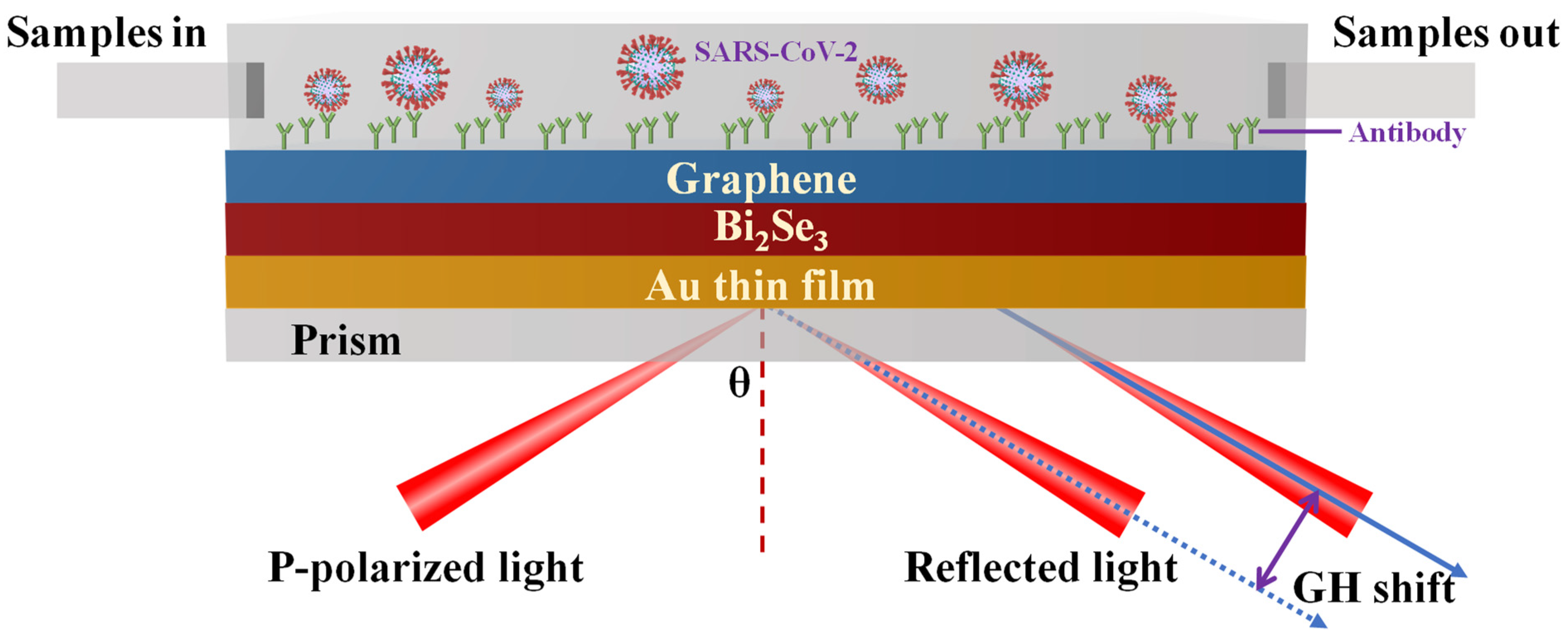
The theoretically proposed SPR biosensor consists of an SF11 prism, an Au thin film, few layered Bi
2Se
3 interlayer and graphene overlayer, as shown in
Figure 1. Firstly, the plasmonic gold film was efficiently integrated with a SF11 prism. It is worth noting that plasmonic metal materials usually suffer from strong energy dissipation because of inter-band electronic transitions [
26]. To further enhance detection sensitivity, it is necessary to supplement low-loss plasmonic materials onto gold film. Considering the vdWs stacked Bi
2Se
3/Graphene heterostructures having high carrier mobility, it was introduced to work as an important plasmonic layer, significantly developing the energy dissipation. Then, Bi
2Se
3 interlayer was vdWs stacked onto the top of plasmonic gold film. After this, few layered graphene overlayer was further stacked onto Bi
2Se
3 interlayer to form Bi
2Se
3/Graphene heterostructures. The topmost layer was a sealed cell containing work solutions. It is worth noting that the work solutions consisting of 10 mM HEPES (4-(2-hydroxyethyl)−1-piperazineethanesulfonic acid) and 120 mM NaCl (sodium chloride) was utilized to contain SARS-CoV−2 and its S glycoprotein in this simulation. To really calculate the binding interaction between SARS-CoV−2 and sensing interface of Bi
2Se
3/Graphene heterostructures, the work buffer consisting of 10 mM HEPES and 120 mM NaCl solutions was injected from left entrance. Once the target analytes in running buffer were bound to the sensing interface, the change in local RI would be different. Generally, the tiny variation in RI could be readout by measuring the change in intensity of reflected light, SPR angle and differential phase. In this work, p-polarized incident light having a wavelength at 632.8 nm was applied to resonate with SPPs wave in Au film/Bi
2Se
3/Graphene heterostructures. Unlike previous SPR biosensors created by phase modulation, our proposed biosensor was designed by measuring GH shift. It is well-known that GH shift is an interesting displacement behavior of reflected light relative to geometric reflection theory, because practical incident lights generated by lasers are not ideal monochromatic electromagnetic plane waves [
27]. Moreover, GH shift can be explained by stationary phase theory [
28], indicating that GH shift was highly related with phase transition of reflected light. Specifically, the GH shift can be obtained by calculating the first derivative of reflected light versus incident angle (Equation (12)). However, the actual GH shifts generated by low RI dielectric interface were only 5~10 μm [
29,
30], which was difficult for experimental measurement. Fortunately, GH shifts could be hugely enhanced using SPR technology [
31,
32]. Under the strongest SPR excitation, phase of reflected light usually experiences a steep jump and GH shift is the first-order derivative of phase. Then, GH shift was supposed to be more sensitive than phase transition under the strongest SPR effects. Therefore, GH shift could work as an important indicator for evaluating biosensing performance for our proposed biosensor. However, compared with other measurement models, including angle-, amplitude-, wavelength- and phase-modulation, large GH shifts usually suffer from a narrow interval for tuning incident angle.
Both photon absorption and energy dissipation in our proposed configuration highly depend on optical dielectric constant of each layer. Prior to biosensing simulation, the dielectric constant of each layer needs to be determined. Under the excitation light of 632.8 nm, the refractive indices of SF11 prism layer, Au film layer, Bi
2Se
3 nanosheets and graphene overlayer is 1.7786 [
33]. 0.1838 + 3.4313i [
7]. 4.2923 + 1.7922i [
34] and 3.000 + 1.1487i [
7], respectively. In addition, the thickness of 1-QL Bi
2Se
3 and monolayer graphene is 0.9725 nm [
34] and 0.34 nm [
35], respectively. Finally, the refractive index of running buffer containing 10 mM HEPES and 120 mM NaCl solution can be calculated by Equation (1):
where y stands for the calculated RI of running buffer and x is the concentration of HEPES solution (mM). In this simulation, 10 mM HEPES solution was added into 120 mM NaCl solution and the refractive index of the running buffer (n
C) can be determined to be 1.3345 [
9]. When S glycoproteins based on SARS-CoV−2 was captured antibody sites on graphene layer, the refractive index of sensing interface based on Bi
2Se
3/Graphene configuration was assumed to be proportional to the concentration of S glycoprotein, which can be calculated by Equation (2):
where
nA is the RI due to the adsorption interaction of S glycoprotein and
nC is the RI of running buffer.
cA is the concentration of S glycoprotein solution. In addition, the parameter (
dn⁄
dc) denotes the increment of refractive index and the value of
dn⁄
dc is usually ~0.186 cm
3•g
−1 for studying protein-protein binding interactions [
36]. For a fixed RI variation in sensing interface, the concentration (
cA) of S glycoproteins can be calculated according to the binding parameter (
dn⁄dc).In addition to SPR reflectivity, change in incident angle and differential phase, change in GH shift generated by plasmonic enhancement in our proposed SPR configuration was systematically simulated using transfer matrix method (TMM) and Fresnel equations in a N-layer stacked model. Theoretically, each layer was supposed to parallel in Z-direction and each layer was considered to be isotropic and non-magnetic. It was assumed that the number of antibody sites on graphene layers was much more than that of S protein. The adsorption sites on graphene overlayer were S protein antibody, which can be employed for specifically capture SARS-CoV−2 using antibody-antigen interactions. Generally, the electromagnetic fields at the first boundary along the tangential direction was supposed to be Z
1 = 0, and the relationship between the last boundary ZN−1 and first boundary Z1 could be given as:
where U and V denote the tangential components of electric fields and magnetic field at the boundary, respectively.
Here, M is a transfer matrix, which can be obtained by the following equation for p-polarized light:
where M
k could be described as:
where
βk and
qk can be determined using the following two Equations (6) and (7):
where k is the k-th stacking layer and
dk stands for the thickness of the k-th layer. Additionally,
εk represents the dielectric constant of the k-th layer. In Equation (7),
θ1 and
n1 are the incident angle and RI of the first stacking layer, respectively.
For s-polarized light, these relationships described above are still practicable. However,
qk was described by Equation (8):
Prior to calculating GH shift, the reflectivity (
Rp) in our proposed configuration can be obtained using Equation (9):
Next, the p-polarized of reflected light phase
φp can be calculated by the following equation:
Therefore, the differential phase Δ
φd can be calculated by Equation (11):
where
φs stands for the phase of s-polarized light.
According to the stationary phase theory, the GH shift (
GHS) can be calculated by Equation (12):
For p-polarized light, the GH shifts produced by metal films are negative. However, the GH shift excited by s-polarized light in metal films are usually positive [
37]. Moreover, the value of GH shift from p-polarized light is much larger than s-polarized light. Similar to the differential phase, the differential GH shift (Δ
GHSd) between p- and s-polarized light can be calculated as follows:
To evaluate the biosensing performance of our proposed configuration, two parameters, such as phase sensitivity (
Sφ) and GH shift sensitivity (S
GHS), were introduced. Both of them can be determined as follows:
where Δ
nbio denotes a tiny variation of RI in sensing interface of Bi
2Se
3/graphene heterostructures due to strong adsorption binding interaction.
3. Results and Discussion
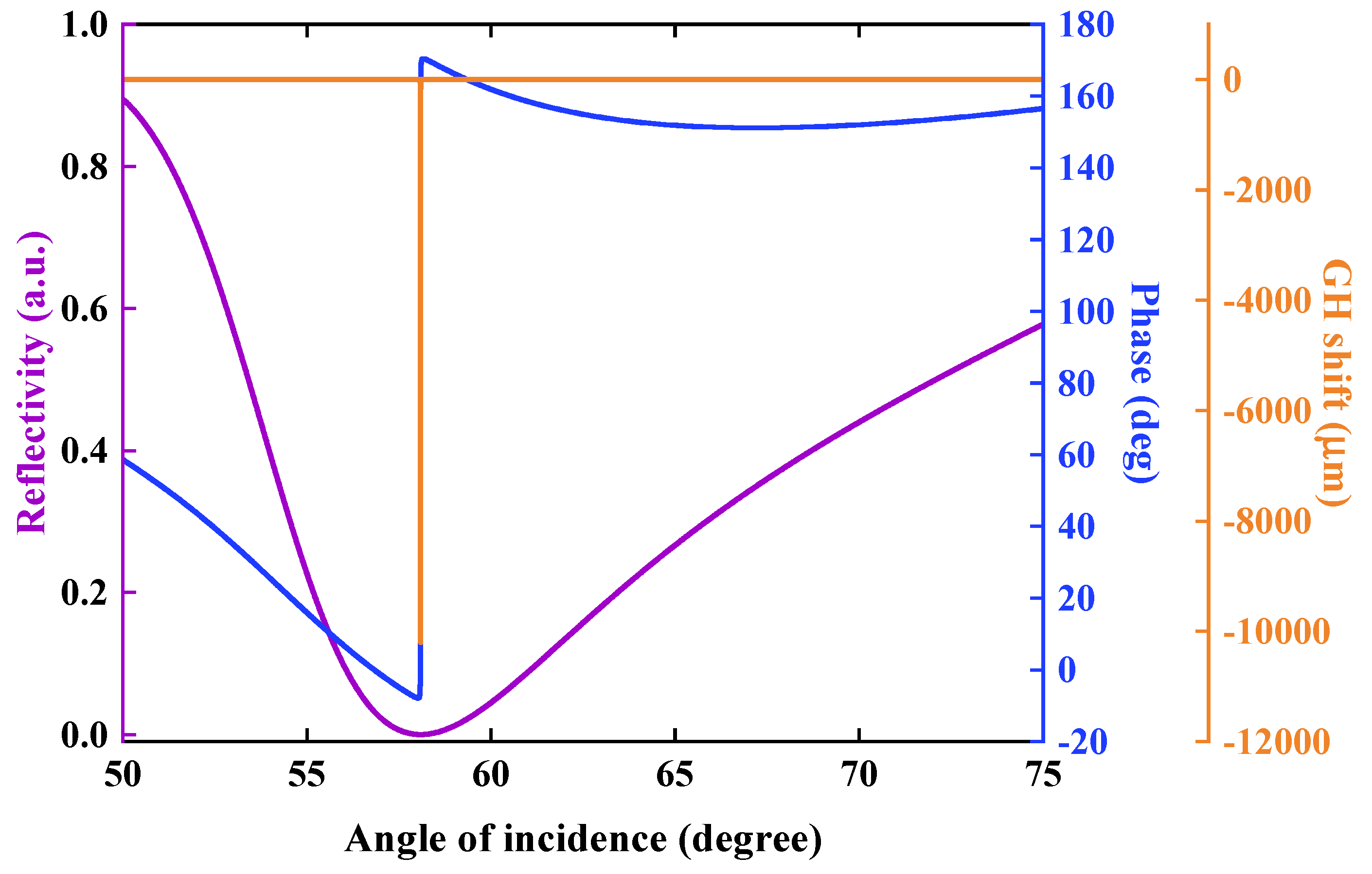
Under the illumination of 632.8 nm, the optimal reflectivity, phase and GH shift was obtained, as shown in
Figure 2. It can be found that when the incident angle is located at 58.0864°, the stacked configuration: 32 nm Au film−2-QL Bi
2Se
3–3-layer graphene can produce an ultralow reflectivity (purple curve,
Figure 2) of 5.4402 × 10
−9, approaching zero. It indicates that almost 100% of photons were absorbed and converted into SPR energy. Meanwhile, the phase produces a sharp transition at the same incident angle (blue curve,
Figure 2), perfectly corresponding to the minimum SPR reflectivity. More importantly, the GH shift showed a sharper transition strength than phase at the point of SPR angle. There was a significant enhanced negative GH shift (orange curve,
Figure 2) in Au film/Bi
2Se
3/graphene heterostructures as high as −1.0202 × 10
4 µm. These observations suggest that a large GH shift is a useful indicator for evaluating biosensing performance.
To further verify sensitivity enhancement ability of our proposed configuration, the GH shift as well as reflectivity, incident angle and phase, were systematically examined by tuning the stacking thickness of Bi
2Se
3/Graphene heterostructures (Bi
2Se
3, 0–5 layers; graphene, 0–5 layers), as shown in
Figure 3. In the absence of Bi
2Se
3/graphene heterostructures, the plasmonic Au film (32 nm) has a reflectivity of 0.2786 under the illumination of 632.8 nm (black dotted curve,
Figure 3a). It means that, single Au film suffers from large energy dissipation. However, the dilemma can be significantly improved by introducing low-loss Bi
2Se
3/Graphene heterostructures. When 2-QLs Bi
2Se
3 film was stacked onto 32 nm Au film, the reflectivity of Au film-Bi
2Se
3 heterostructures could be decreased to 0.0065 (blue curve,
Figure 3a). Moreover, as 3-layer graphene was stacked, the SPR reflectivity (blue curve,
Figure 3d) of gold film/Bi
2Se
3/graphene heterostructures could be lowered to 5.4402 × 10
−9. In addition, there were obvious red-shifts in incident angle, due to the addition of Bi
2Se
3/Graphene heterostructures. Interestingly, the obtained reflectivity of 5.4402 × 10
−9 corresponds to the optimal incident angle at 58.0864°. Meanwhile, phase from reflected light also experienced a Heaviside step-like transition, as shown in
Figure 3b–e. Moreover, it showed the steepest phase singularity as the plasmonic configuration biosensor was stacked as 32 nm Au film−2-QL Bi
2Se
3-3-layer graphene. At the phase singularity, the GH shift can be obtained by calculating the derivative of phase with respect to incident angle. It can be found that the largest GH shift of −1.0202 × 10
4 µm is generated by 32 nm Au film-2-QL Bi
2Se
3-3-layer graphene, as shown in
Figure 3f. Interestingly, with increasing graphene layers, the value of GH shift changes from positive to negative, which is synchronized with phase transition.
Figure 3f showed that as the number of Bi
2Se
3 QLs is from 0 to 5, the obtained GH shift is 5.4312, 7.3689, −1.0202 × 10
4, −3.9267, −1.5591 and −0.8831 µm, respectively. However,
Figure 3f also showed that a tunable interval of incident angle for obtaining multiple large differential GH shift is narrow. The reason is that, at the dip of minimum SPR reflectivity, both phase and GH shift of reflected light usually experience significant transition behavior. Moreover, GH shift was obtained by derivating phase with respect to incident angle (Equation (12)). Thus, the GH shift shows a sharper transition strength than phase. The narrow interval of incident angle seems that it will be difficult for performing practical measurement. According to phase-modulation theory, once an optimal incident angle is fixed, both largest differential phase and GH shift will be determined. To perform practical GH measurements, it needs to fix at an optimal incident angle rather than vary incident angle.
To study the biosensing ability of our proposed biosensor, both differential phase (Δ
φd) and GH shift (Δ
GHSd) response for a defined RIU variation (Δ
nbio = 0.0012) were plotted, as shown in
Figure 4a,b. The largest differential phase (green curve,
Figure 4a) is 84.3891°, generated from the configuration of 32 nm Au film/2QL-Bi
2Se
3/3-layer graphene.
Figure 4b showed the change in differential GH shift (Δ
GHSd) by changing the number of Bi
2Se
3 and graphene layers. The configuration of 32 nm Au film-Bi
2Se
3 (2 QL)-graphene (3 layer) provides the highest differential GH shift of 1.0202 × 10
4 µm (green curve), which is almost 324 times larger than the second highest differential GH shift of 31.466 µm (blue curve) generated by the configuration of 32 nm Au film/2-QL Bi
2Se
3/2-layer graphene. When the number of Bi2Se3 QLs is 2, the phase detection sensitivity obtained by varying the number of graphene overlayer are almost on the same order of magnitude of 10
4°/RIU, as shown in
Figure 4c. However, the difference in differential phase can be hugely amplified by further calculating derivative of phase. Thus, the obtained GH shift detection sensitivity shows a larger difference than phase detection sensitivity, as shown in
Figure 4d. Thus, the change in GH shift was more significant compared to phase modulation.
In addition, we also studied the changes in incident angle (Δ
θSPR) for a defined RIU variation (Δ
nbio = 0.0012), as shown in
Figure S1. There was only a response of 0.0126° for red-shift in SPR angle. However, such tiny red-shifts in SPR angle cannot be distinguished by an optical detector. Conversely, both differential phase and GH shift can be employed to monitor the RI variation of sensing interface. Afterwards, the obtained largest phase sensitivity was 7.0324 × 10
4 degree/RIU, as shown in
Figure 4c. In contrast,
Figure 4d showed the largest GH shift sensitivity could reach the value of 8.5017 × 10
6 µm/RIU. It is generally agreed that such a large GH shift can be easily detected by common optical devices. Compared with other reported GH shift-based plasmonic configurations (
Table 1), our proposed biosensor exhibited higher detection sensitivity. In addition, considering that few-layered Bi
2Se
3 nanosheets have the advantages of simple fabrication and low cost [
38], our proposed biosensor will be inexpensive and easily fabricated.
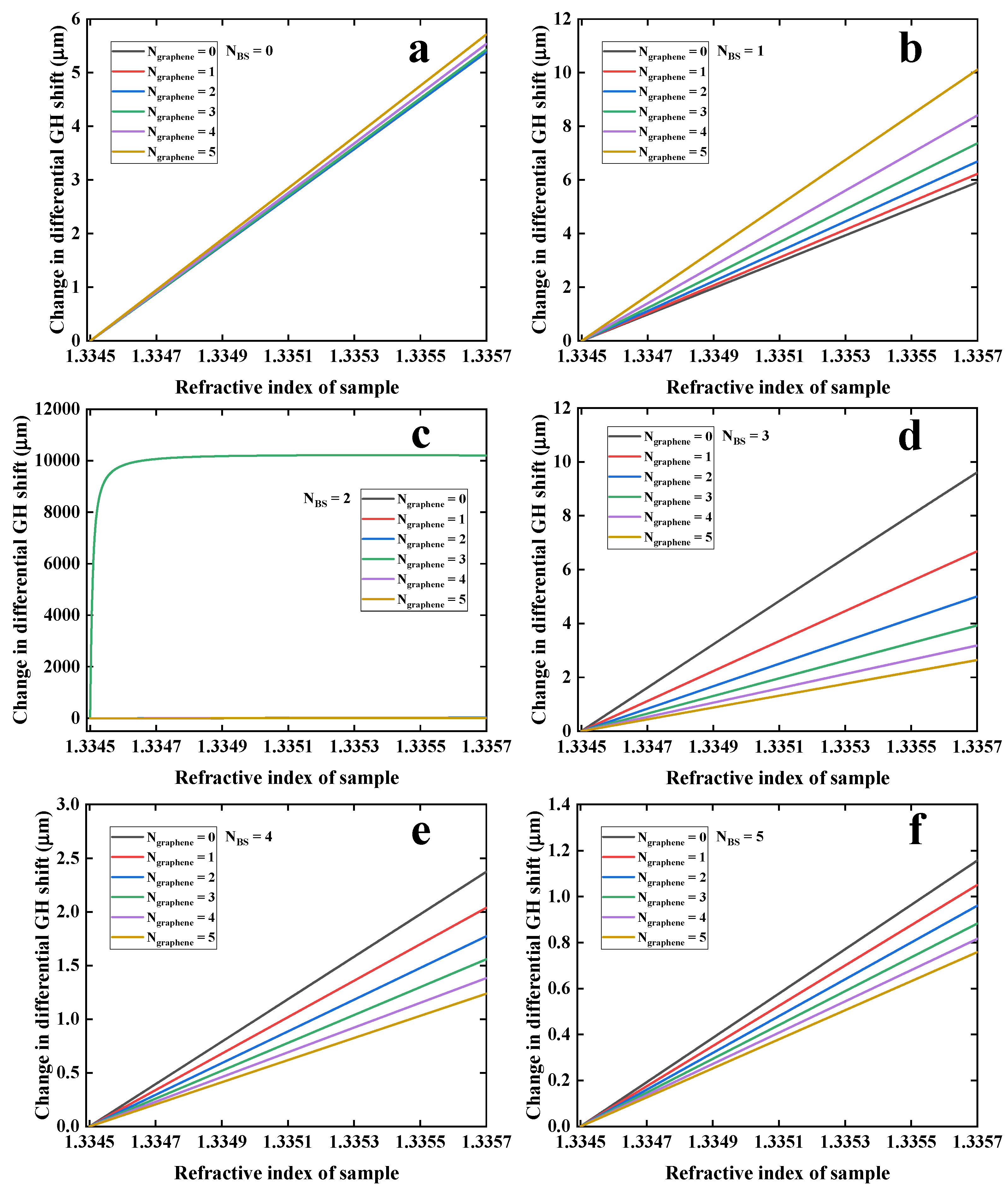
Next, the detailed changes in differential GH shift for the RI from 1.3345 to 1.3357 RIU by tuning the number of Bi
2Se
3 QLs (0–5) and graphene overlayers (0–5) were studied, as shown in
Figure 5. When the number of Bi
2Se
3 layers was less than 2, there was a good linear response for change in differential GH shift by changing the RI of sensing interface. Obviously, the obtained GH shift was relative weak, indicating that there was no significant SPR enhancement effects, as shown in
Figure 5a,b. However, when the number of Bi
2Se
3 layers is 2, the addition of 3-layer graphene can precipitously produce an ultrasensitive response, as shown in
Figure 5c. When the number of Bi
2Se
3 layers was larger than 2, the addition of graphene overlayer could not provide a positive response because of excessive energy loss. It can be concluded that the configuration of 32 nm Au film coated with two-QL Bi
2Se
3 and three-layer graphene has the strongest GH shift response, showing great promise for performing ultrasensitive biosensing for a tiny RI variation.
To quantitatively monitor the concentrations of target analytes, it is necessary to determine a linear response interval for our optimal plasmonic configuration: 32 nm Au film−2-QL Bi
2Se
3-3-layer graphene.
Figure S2 showed a linear response of GH shift for a tiny RI variation as small as 10
−6 RIU. In contrast to 32 nm Au thin film, 3-layer graphene coated on 32 nm Au film, the optimal configuration: 32 nm Au film−2-QL Bi
2Se
3-3-layer graphene can provide an enhancement factor (EF) of 2 × 10
5. It was assumed that significantly local field intensity enhancement should contribute to obtain such a high EF. It is well-known that typical nanoscale heterogeneous configurations, such as C-shaped [
40], Φ-shaped [
41], bowtie-shaped [
42] and ring-shaped [
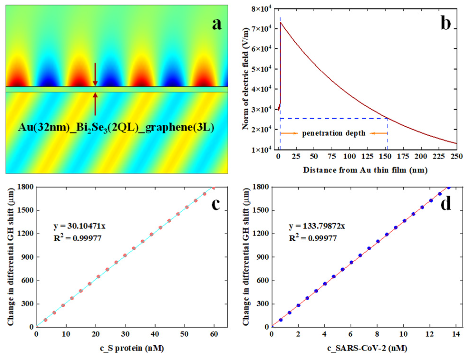
43] nanostructures, have shown significant field enhancement. To verify the proposal for producing such a high EF, the electric field distribution of 32 nm Au film−2-QL Bi
2Se
3-3-layer graphene was further simulated via finite element analysis method, as shown in
Figure 6a,b. It clearly showed that, under the illumination of 632.8 nm, there was a significantly enhanced electric field close to the Bi
2Se
3/graphene sensing interface. Moreover, the electric field intensity decayed exponentially into a running buffer, resulting in a penetration depth of 150 nm. In addition, the charge-transfer mechanism generated by difference in work function (Fermi level) was proposed to contribute to giant electric field enhancement. It has been reported that the work function of Au film is ~5.54 eV and the work function of 2-QL Bi
2Se
3-3-layer graphene is ~4.75 eV [
22]. The large difference in work function can induce strong band bending, eventually resulting in strong charge-transfer. Thus, the direct-write orientation of charge transfer in optimal configuration would be from Bi
2Se
3/Graphene heterostructures to Au thin film.
Employing the linear response interval of 32 nm Au film-2-QL Bi
2Se
3-3-layer graphene, the feasibility of monitoring SARS-CoV-2 and its S protein was theoretically studied. It was predicted that the molecular weight (MW) of SARS-CoV-2 is approximately 800 kDa [
44], which is much larger than that of S protein 180 kDa [
45]. According to Equation (2), linear relationships between change in differential GH shift (µm) and detection concentration (nM) of adsorbed analytes were plotted, as shown in
Figure 6c,d. For a minor RI variation of 0.000002 RIU, a good linear detection interval (
Figure 6c) for S protein is from 0 to 59.74 nM, which is described by an equation Δ
GHSd = 30.1047 *c
Sprotein. Here, the
cSprotein denotes the concentration of S protein solution. More importantly, our proposed biosensor also exhibited an excellent response interval (0–13.44 nM) for quantitatively monitoring SARS-CoV−2. The linear response can be expressed by such an equation Δ
GHSd = 133.7987 *
cSARS-CoV−2, where
cSARS-CoV−2 stands for the concentration of SARS-CoV−2 solution. Therefore, our proposed plasmonic biosensor has shown great feasibility in quantitatively monitoring SARS-CoV-2 and its S protein.


