
Organic Solar Cells Improved by Optically Resonant Silicon Nanoparticles
 , , ,
, , , 
Abstract
:1. Introduction
2. Results
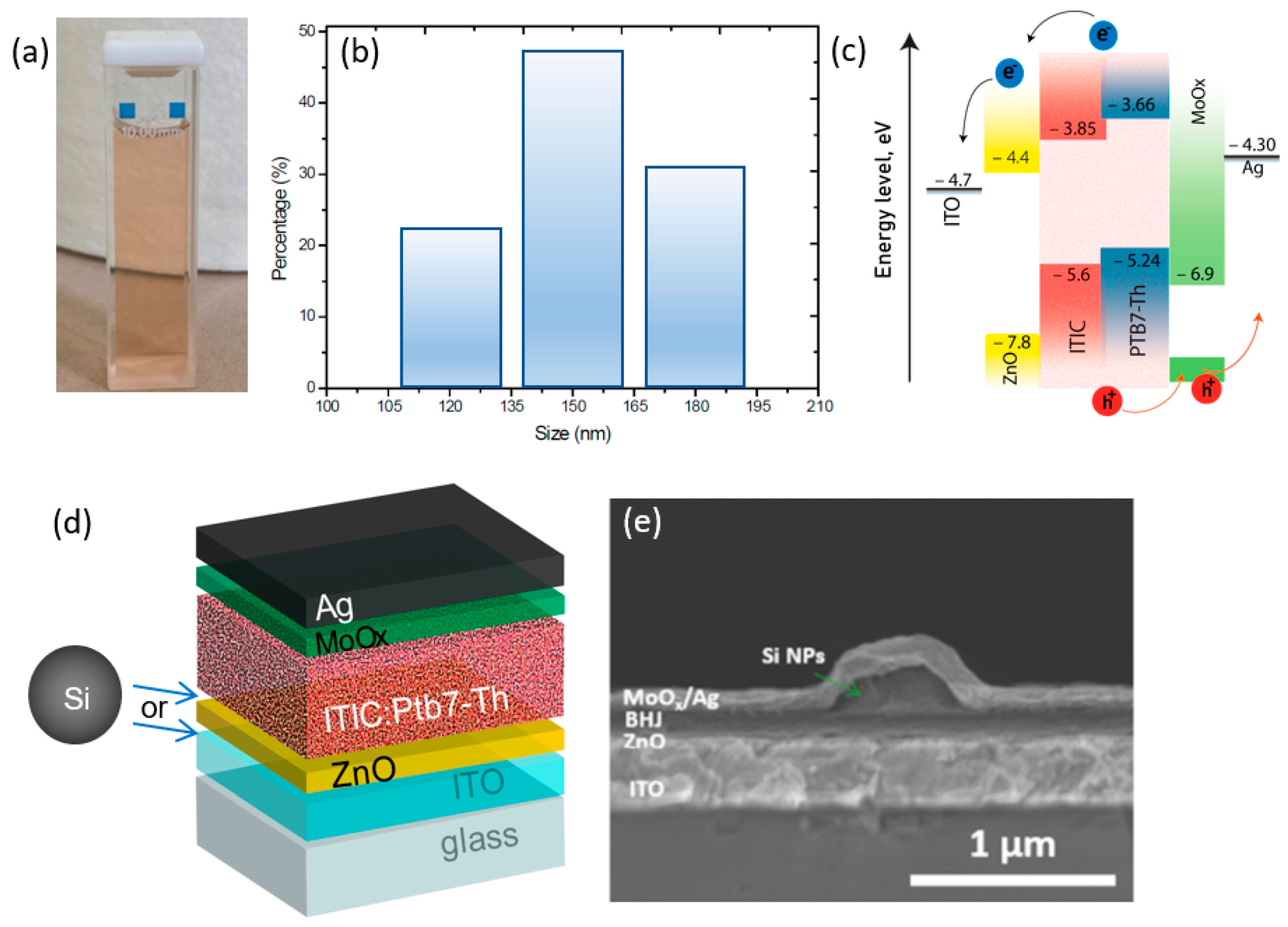
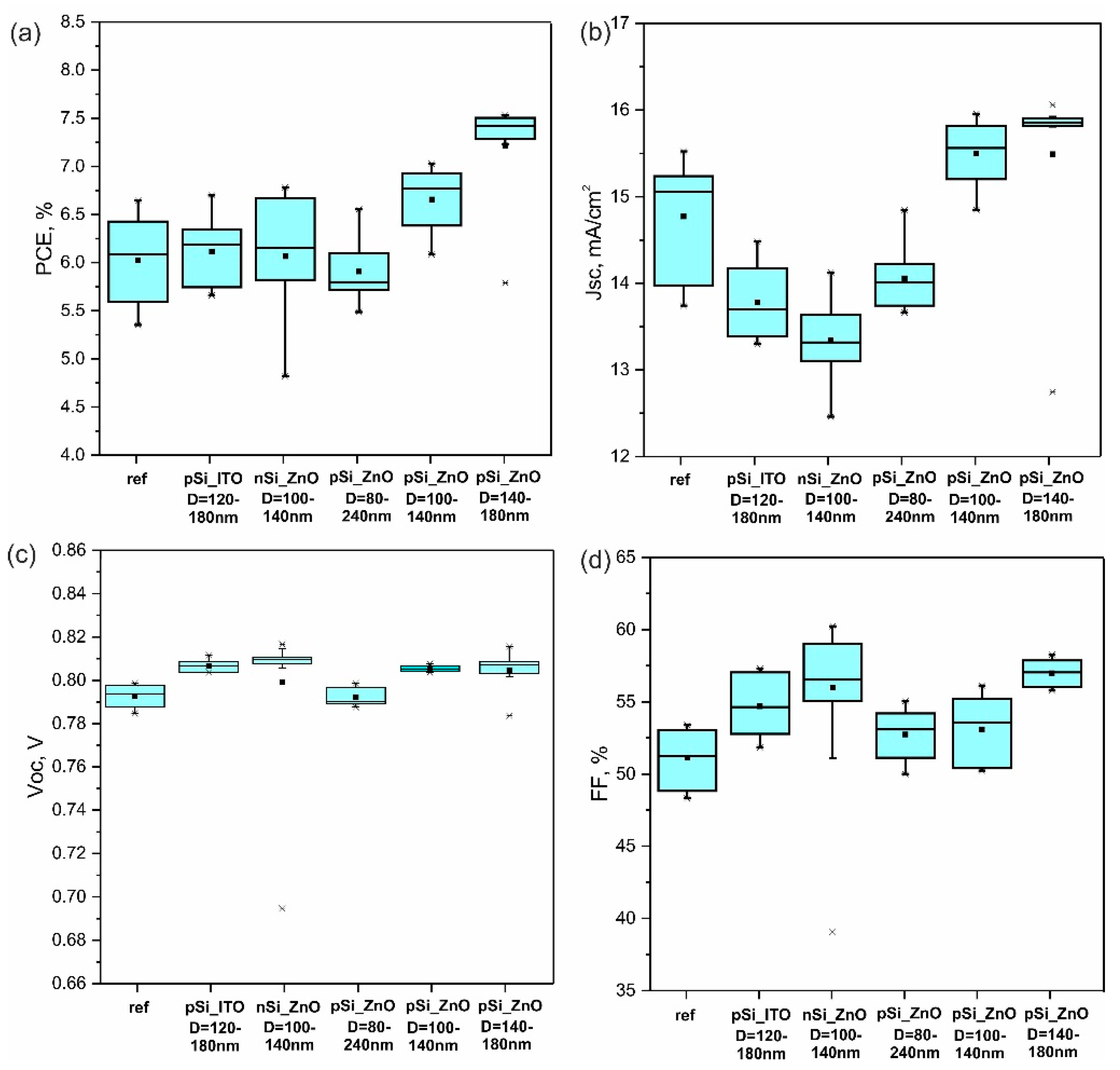
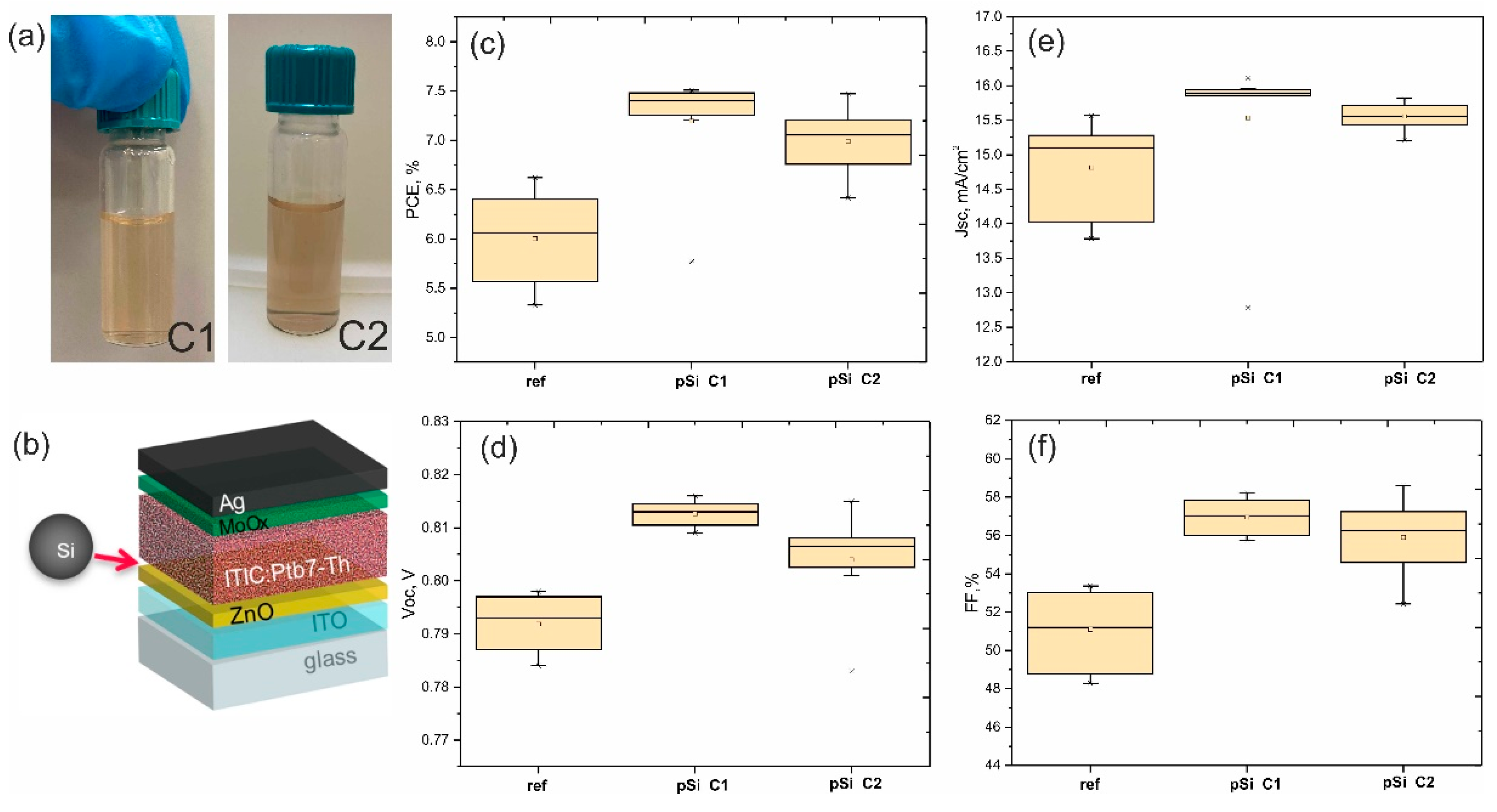
2.1. Samples
2.2. Devices Fabrication and Characterization
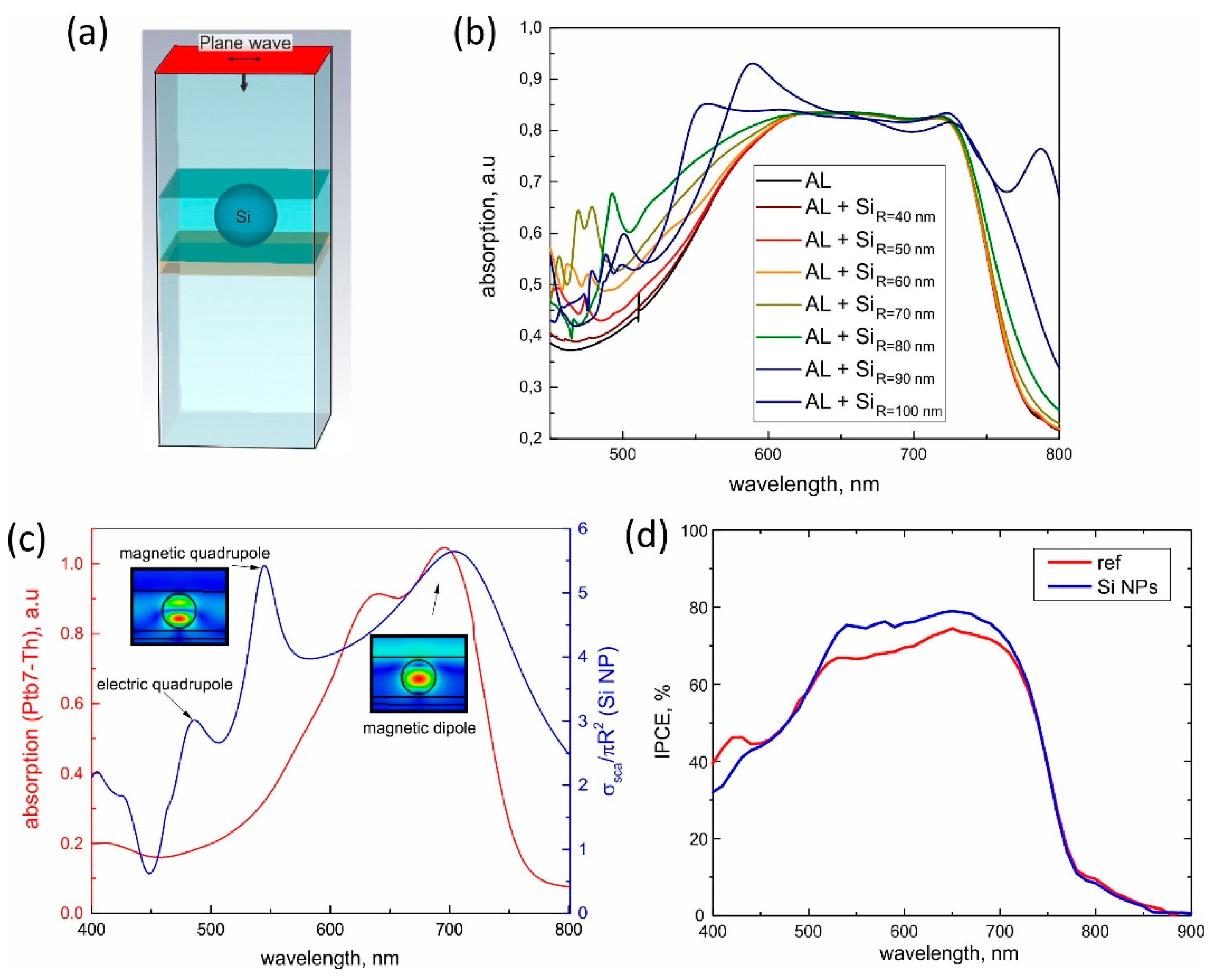
2.3. Discussion
3. Conclusions
Supplementary Materials
Author Contributions
Funding
Data Availability Statement
Acknowledgments
Conflicts of Interest
References
- Hoppe, H.; Sariciftci, N.S. Organic solar cells: An overview. J. Mater. Res. 2004, 19, 1924–1945. [Google Scholar] [CrossRef] [Green Version]
- Hu, Z.; Wang, J.; Ma, X.; Gao, J.; Xu, C.; Yang, K.; Wang, Z.; Zhang, J.; Zhang, F. A critical review on semitransparent organic solar cells. Nano Energy 2020, 78, 105376. [Google Scholar] [CrossRef]
- Choi, J.Y.; Park, I.P.; Heo, S.W. Ultra-Flexible Organic Solar Cell Based on Indium-Zinc-Tin Oxide Transparent Electrode for Power Source of Wearable Devices. Nanomaterials 2021, 11, 2633. [Google Scholar] [CrossRef] [PubMed]
- Inganäs, O. Organic photovoltaics over three decades. Adv. Mater. 2018, 30, 1800388. [Google Scholar] [CrossRef] [PubMed]
- Lewis, N.S. Research opportunities to advance solar energy utilization. Science 2016, 351, add1920. [Google Scholar] [CrossRef] [Green Version]
- Ko, D.H.; Tumbleston, J.R.; Gadisa, A.; Aryal, M.; Liu, Y.; Lopez, R.; Samulski, E.T. Light-trapping nano-structures in organic photovoltaic cells. J. Mater. Chem. 2011, 21, 16293–16303. [Google Scholar] [CrossRef]
- Stratakis, E.; Kymakis, E. Nanoparticle-based plasmonic organic photovoltaic devices. Mater. Today 2013, 16, 133–146. [Google Scholar] [CrossRef]
- Guo, Q.; Guo, Q.; Geng, Y.; Tang, A.; Zhang, M.; Du, M.; Sun, X.; Zhou, E. Recent advances in PM6: Y6-based organic solar cells. Mater. Chem. Front. 2021, 5, 3257–3280. [Google Scholar] [CrossRef]
- Che, X.; Li, Y.; Qu, Y.; Forrest, S.R. High fabrication yield organic tandem photovoltaics combining vacuum-and solution-processed subcells with 15% efficiency. Nat. Energy 2018, 3, 422–427. [Google Scholar] [CrossRef]
- Zhao, S.; Pi, X.; Mercier, C.; Yuan, Z.; Sun, B.; Yang, D. Silicon-nanocrystal-incorporated ternary hybrid solar cells. Nano Energy 2016, 26, 305–312. [Google Scholar] [CrossRef]
- Ou, Q.D.; Li, Y.Q.; Tang, J.X. Light manipulation in organic photovoltaics. Adv. Sci. 2016, 3, 1600123. [Google Scholar] [CrossRef] [PubMed]
- Maier, S.A. Plasmonics: Fundamentals and Applications; Springer: New York, NY, USA, 2007; Volume 1, p. 245. [Google Scholar]
- Schuller, J.A.; Barnard, E.S.; Cai, W.; Jun, Y.C.; White, J.S.; Brongersma, M.L. Plasmonics for extreme light concentration and manipulation. Nat. Mater. 2010, 9, 193–204. [Google Scholar] [CrossRef] [PubMed]
- Atwater, H.A.; Polman, A. Plasmonics for improved photovoltaic devices. Nat. Mater. 2010, 9, 205–213. [Google Scholar] [CrossRef] [PubMed]
- Pillai, S.A.; Green, M.A. Plasmonics for photovoltaic applications. Sol. Energy Mater. Sol. Cells 2010, 94, 1481–1486. [Google Scholar] [CrossRef]
- Wen, C.; Ishikawa, K.; Kishima, M.; Yamada, K. Effects of silver particles on the photovoltaic properties of dye-sensitized TiO2 thin films. Sol. Energy Mater. Sol. Cells 2000, 61, 339–351. [Google Scholar] [CrossRef]
- Brown, M.D.; Suteewong, T.; Kumar, R.S.S.; D’Innocenzo, V.; Petrozza, A.; Lee, M.M.; Wiesner, U.; Snaith, H.J. Plasmonic dye-sensitized solar cells using core− shell metal− insulator nanoparticles. Nano Lett. 2011, 11, 438–445. [Google Scholar] [CrossRef] [PubMed]
- Ding, I.; Zhu, J.; Cai, W.; Moon, S.-J.; Cai, N.; Wang, P.; Zakeeruddin, S.M.; Grätzel, M.; Brongersma, M.L.; Cui, Y. Plasmonic dye-sensitized solar cells. Adv. Energy Mater. 2010, 1, 52–57. [Google Scholar] [CrossRef]
- Derkacs, D.; Lim, S.H.; Matheu, P.; Mar, W.; Yu, E.T. Improved performance of amorphous silicon solar cells via scattering from surface plasmon polaritons in nearby metallic nanoparticles. Appl. Phys. Lett. 2006, 89, 093103. [Google Scholar] [CrossRef] [Green Version]
- Pillaia, S.; Catchpole, K.R.; Trupke, T.; Green, M.A. Surface plasmon enhanced silicon solar cells. J. Appl. Phys. 2007, 101, 093105. [Google Scholar] [CrossRef]
- Hayashi, S.; Kozaru, K.; Yamamoto, K. Enhancement of photoelectric conversion efficiency by surface plasmon excitation: A test with an organic solar cell. Solid State Commun. 1991, 79, 763–767. [Google Scholar] [CrossRef]
- Gan, Q.; Bartoli, F.J.; Kafafi, Z.H. Plasmonic-enhanced organic photovoltaics: Breaking the 10% efficiency barrier. Adv. Mater. 2013, 25, 2385–2396. [Google Scholar] [CrossRef] [PubMed]
- Vangelidis, I.; Theodosi, A.; Beliatis, M.J.; Gandhi, K.K.; Laskarakis, A.; Patsalas, P.; Logothetidis, S.; Silva, S.R.P.; Lidorikis, E. Plasmonic organic photovoltaics: Unraveling plasmonic enhancement for realistic cell geometries. ACS Photonics 2018, 5, 1440–1452. [Google Scholar] [CrossRef]
- Furasova, A.; Voroshilov, P.; Sapori, D.; Ladutenko, K.; Barettin, D.; Zakhidov, A.; Di Carlo, A.; Simovski, C.; Makarov, S. Nanophotonics for Perovskite Solar Cells. Adv. Photonics Res. 2022, 3, 2100326. [Google Scholar] [CrossRef]
- Kuznetsov, A.I.; Miroshnichenko, A.E.; Brongersma, M.L.; Kivshar, Y.S.; Luk’yanchuk, B. Optically resonant dielectric nanostructures. Science 2016, 354, aag2472. [Google Scholar] [CrossRef] [PubMed] [Green Version]
- Staude, I.; Schilling, J. Metamaterial-inspired silicon nanophotonics. Nat. Photonics 2017, 11, 274–284. [Google Scholar] [CrossRef]
- Zograf, G.P.; Petrov, M.I.; Makarov, S.V.; Kivshar, Y.S. All-dielectric thermonanophotonics. Adv. Opt. Photonics 2021, 13, 643–702. [Google Scholar] [CrossRef]
- Zywietz, U.; Evlyukhin, A.B.; Reinhardt, C.; Chichkov, B.N. Laser printing of silicon nanoparticles with resonant optical electric and magnetic responses. Nat. Commun. 2014, 5, 3402. [Google Scholar] [CrossRef] [Green Version]
- Furasova, A.; Voroshilov, P.; Baranov, M.; Tonkaev, P.; Nikolaeva, A.; Voronin, K.; Vesce, L.; Makarov, S.; Di Carlo, A. Mie-resonant mesoporous electron transport layer for highly efficient perovskite solar cells. Nano Energy 2021, 89, 106484. [Google Scholar] [CrossRef]
- Sain, B.; Meier, C.; Zentgraf, T. Nonlinear optics in all-dielectric nanoantennas and metasurfaces: A review. Adv. Photonics 2019, 1, 024002. [Google Scholar] [CrossRef] [Green Version]
- Hemaprabha, E.; Pandey, U.K.; Chattopadhyay, K.; Ramamurthy, P.C. Doped silicon nanoparticles for enhanced charge transportation in organic- inorganic hybrid solar cells. Sol. Energy 2018, 173, 744–751. [Google Scholar] [CrossRef]
- Zhang, D.; Gokce, B.; Barcikowski, S. Laser synthesis and processing of colloids: Fundamentals and applications. Chem. Rev. 2017, 117, 3990–4103. [Google Scholar] [CrossRef] [PubMed]
- Zyuzin, M.V.; Baranov, D.G.; Escudero, A.; Chakraborty, I.; Tsypkin, A.; Ushakova, E.V.; Kraus, F.; Parak, W.J.; Makarov, S.V. Photoluminescence quenching of dye molecules near a resonant silicon nanoparticle. Sci. Rep. 2018, 8, 6107. [Google Scholar] [CrossRef] [PubMed] [Green Version]
- Feng, L.; Niu, M.; Wen, Z.; Hao, X. Recent advances of plasmonic organic solar cells: Photophysical investigations. Polymers 2018, 10, 123. [Google Scholar] [CrossRef] [PubMed] [Green Version]
- Furasova, A.; Calabró, E.; Lamanna, E.; Tiguntseva, E.; Ushakova, E.; Ubyivovk, E.; Mikhailovskii, V.; Zakhidov, A.; Makarov, S.; Di Carlo, A. Resonant silicon nanoparticles for enhanced light harvesting in halide perovskite solar cells. Adv. Opt. Mater. 2018, 6, 1800576. [Google Scholar] [CrossRef]
- Li, M.; Li, J.; Wang, J.; Yu, L.; Wang, T.; Jin, J.; Zheng, C.; Chen, R.; Huang, W. Enhancing Photovoltaic Performance by Cathode Interfacial Modification with Inorganic/Organic Gradient Diffusion Structures. ACS Sustain. Chem. Eng. 2019, 7, 12261–12269. [Google Scholar] [CrossRef]
- Kuznetsov, A.I.; Miroshnichenko, A.E.; Fu, Y.H.; Zhang, J.; Luk’Yanchuk, B. Magnetic light. Sci. Rep. 2012, 2, 492. [Google Scholar] [CrossRef] [Green Version]
- Evlyukhin, A.B.; Novikov, S.M.; Zywietz, U.; Eriksen, R.L.; Reinhardt, C.; Bozhevolnyi, S.I.; Chichkov, B.N. Demonstration of magnetic dipole resonances of dielectric nanospheres in the visible region. Nano Lett. 2012, 12, 3749–3755. [Google Scholar] [CrossRef]
- Evlyukhin, A.B.; Reinhardt, C.; Chichkov, B.N. Multipole light scattering by nonspherical nanoparticles in the discrete dipole approximation. Phys. Rev. B 2011, 84, 235429. [Google Scholar] [CrossRef]
- Zograf, G.P.; Petrov, M.I.; Zuev, D.A.; Dmitriev, P.A.; Milichko, V.A.; Makarov, S.V.; Belov, P.A. Resonant nonplasmonic nanoparticles for efficient temperature-feedback optical heating. Nano Lett. 2017, 17, 2945–2952. [Google Scholar] [CrossRef]
- Furasova, A.; Voroshilov, P.; Lamanna, E.; Mozharov, A.; Tsypkin, A.; Mukhin, I.; Barettin, D.; Ladutenko, K.; Zakhidov, A.; Di Carlo, A.; et al. Engineering the charge transport properties of resonant silicon nanoparticles in perovskite solar cells. Energy Technol. 2020, 8, 1900877. [Google Scholar] [CrossRef]
- Obraztsova, A.A.; Barettin, D.; Furasova, A.D.; Voroshilov, P.M.; Auf der Maur, M.; Orsini, A.; Makarov, S.V. Light-Trapping Electrode for the Efficiency Enhancement of Bifacial Perovskite Solar Cells. Nanomaterials 2022, 12, 3210. [Google Scholar] [CrossRef] [PubMed]
- Gurney, R.S.; Lidzey, D.G.; Wang, T. A review of non-fullerene polymer solar cells: From device physics to morphology control. Rep. Prog. Phys. 2019, 82, 036601. [Google Scholar] [CrossRef] [PubMed]
- Kerremans, R.; Kaiser, C.; Li, W.; Zarrabi, N.; Meredith, P.; Armin, A. The Optical Constants of Solution-Processed Semiconductors—New Challenges with Perovskites and Non-Fullerene Acceptors. Adv. Opt. Mater. 2020, 8, 2000319. [Google Scholar] [CrossRef]
- Usmani, B.; Ranjan, R.; Prateek; Gupta, S.K.; Gupta, R.K.; Nalwa, K.S.; Garg, A. Inverted PTB7-Th:PC71BM organic solar cells with 11.8% PCE via incorporation of gold nanoparticles in ZnO electron transport layer. Sol. Energy 2021, 214, 220–230. [Google Scholar] [CrossRef]


Publisher’s Note: MDPI stays neutral with regard to jurisdictional claims in published maps and institutional affiliations. |
© 2022 by the authors. Licensee MDPI, Basel, Switzerland. This article is an open access article distributed under the terms and conditions of the Creative Commons Attribution (CC BY) license (https://creativecommons.org/licenses/by/4.0/).
Share and Cite
Sandzhieva, M.; Khmelevskaia, D.; Tatarinov, D.; Logunov, L.; Samusev, K.; Kuchmizhak, A.; Makarov, S.V. Organic Solar Cells Improved by Optically Resonant Silicon Nanoparticles. Nanomaterials 2022, 12, 3916. https://doi.org/10.3390/nano12213916
Sandzhieva M, Khmelevskaia D, Tatarinov D, Logunov L, Samusev K, Kuchmizhak A, Makarov SV. Organic Solar Cells Improved by Optically Resonant Silicon Nanoparticles. Nanomaterials. 2022; 12(21):3916. https://doi.org/10.3390/nano12213916
Chicago/Turabian StyleSandzhieva, Maria, Darya Khmelevskaia, Dmitry Tatarinov, Lev Logunov, Kirill Samusev, Alexander Kuchmizhak, and Sergey V. Makarov. 2022. "Organic Solar Cells Improved by Optically Resonant Silicon Nanoparticles" Nanomaterials 12, no. 21: 3916. https://doi.org/10.3390/nano12213916